Multi-channel discharge characteristics cutting by ultra-fine wire-EDM
Ming ZHANG,Zhidong LIU,Hongwei PAN,Cong DENG,Mingbo QIU
College of Mechanical and Electrical Engineering,Nanjing University of Aeronautics and Astronautics,Nanjing 210016,China
KEYWORDS HSWEDM;Multi-channel;Recast layer;Surface roughness;Ultra-fine wire
Abstract Compared with a copper wire electrode,molybdenum wire with a poor conductor is usually used as the electrode in high speed wire-cut electrical discharge machining(HSWEDM),so the resistance of an ultra-fine wire cannot be ignored.To study the differences of discharge characteristics between the ultra-fine wire and the conventional diameter wire,the continuous discharge waveform of two kinds of wire electrodes was compared.It was found that there was a multichannel discharge phenomenon in the discharge waveform cutting by ultra-fine wire.Through the establishment of a discharge equivalent circuit model and the simulation analysis of the electrostatic field,it was found that the reason why ultra-fine wire is easy to form multi-channel discharge phenomenon is that the potential difference between the wire and the workpiece increased linearly along the axis of the wire.Besides,etching products like metal particles will distort the electric field between the electrodes.Both of them make it easy to form a multi-channel discharge in machining.The results show that the distributions of the equivalent resistance and the peak current are affected by the multi-channel discharge position.Multi-channel discharge can disperse energy and increase effective discharge frequency.Compared with the 0 mm spacing,at a spacing of 100 mm,the machining efficiency increases by 8.7%,the surface roughness decreases by 37.7%,and the average recast layer thickness decreases by 46.6% under the condition of ultra-fine wire-EDM.
1.Introduction
Due to non-contact machining,controllable single discharge energy,and the improvement in the production process of fine wire electrode,wire-cut electrical discharge machining(WEDM) plays an irreplaceable role in the molding industry with a large aspect ratio and high matching precision,as well as with the machining of micro and complex micro-electromechanical system (MEMS) parts.According to the traditional electrical discharge machining (EDM) theory,each pulse will produce a pulse discharge between the electrode and the workpiece.However,it has been found that under specific machining conditions,a single pulse can form a multi-channel discharge,which plays a positive role in improving the efficiency and the surface quality of EDM.
Kunieda and Muto used the same circuit structure as the double electrode discharge system to realize multi-spark machining,and timely changed the polarity to balance the difference in the material removal rate (MRR) between the two electrodes.It was found that,compared with the traditional EDM,the multi-spark method presented less wear and surface roughness at a higher MRR and pulse utilization rate.Yang et al.divided the tool electrode into several insulated electrodes and respectively coupled them with capacitance to realize multi-spark EDM.Through theoretical analysis and circuit simulation,it was found that the MRR increased with the increase in the number of segmented electrodes.Similarly,Mohri et al.connected multiple insulated electrodes in a series with resistors to achieve a multi-channel discharge.Yu et al.also found the existence of a multi-channel discharge in EDM ablation machining by connecting several insulated tubular electrodes and resistors in the series.The realization of the multi-channel discharge in the literatures mentioned above are mostly achieved by connecting external capacitance or resistance to improve the potential difference between the electrode and the workpiece,thus obtaining multiple breakdowns of the dielectric between electrodes.Huang found that the potential difference between the sampling point and the wire electrode increased with the increase of the spacing between the measuring point and conductive block.However,there is still a large potential difference outside of the discharge point because of the large bulk resistance of silicon.Therefore,during a pulse voltage,the spark discharge may be produced at a position far away from the discharge point.Based on this principle,Qiu et al.used silicon as a tool electrode and verified that the potential far away from the discharge point is high,causing the formation of multi-channel discharge.Sun et al.used a conductive glass with a certain resistance value for powder mixed machining and found that there were multiple discharges in a single pulse time.The average number of discharge channels was closely related to the power supply voltage,and there was an optimal voltage amplitude.The average number of discharge points produced by a single pulse is independent of pulse width,but it does not further explain the effect of electrode resistance on the multichannel discharge.Moreover,the research on the multichannel discharge mainly focuses on traditional EDM.However,it is difficult to realize multi-channel discharge by changing the tool electrode form due to the high wire moving speed for HSWEDM.Chen et al.studied the multi-channel discharge phenomenon in semiconductor processing by HSWEDM.It was considered that the multi-channel production was due to the existence of large body resistance and contact barrier.If a large resistance is added to the workpiece to imitate the characteristics of semiconductor,the utilization rate of pulse power supply and processing efficiency will be greatly reduced.Therefore,there is little research on multi-channel discharge characteristics on WEDM.About ultra-fine wire processing,Zhang et al.studied the phenomenon of wire electrical dischargeelectrochemical machining in water-based composite working fluid by using ultra-fine wire.Qu et al.proposed that axial electrolyte flushing can improve the stability of wire electrode electrochemical machining.Zhang et al.proposed that variable amplitude pulse can be used in the hybrid electrochemical discharge process to improve the surface quality and machining precision of superalloys.However,the above research is still based on the traditional electrical machining characteristics.
By analyzing the discharge model of an ultra-fine wire,it was found that there was still a high potential difference between the wire and the workpiece outside of the discharge point.Moreover,the electric field between electrodes will be distorted by the etching products.Therefore,the discharge characteristics of ultra-fine wire-EDM will be different from those of traditional WEDM which uses the molybdenum wire with a diameter of 0.18 mm for machining.In order to facilitate the study of multi-channel discharge,two thin workpieces with variable spacing are selected to constrain the discharge position,and the number of them is counted by the designed FPGA device.Based on this,it is found that the multichannel discharge affects the peak current and discharge frequency on the workpiece thickness,and also affects the machining efficiency,surface roughness and recast layer thickness.
2.Experimental device
In order to meet the requirements of ultra-fine wire cutting,the machine tool has been redesigned and its performance has been verified.The schematic diagram of the experimental device is presented in Fig.1.Due to the randomness of the discharge point,even if the multi-channel discharge phenomenon occurs on a workpiece,the waveform cannot be collected through the oscilloscope.Two workpieces are used to verify the existence of multi-channel discharge in machining.Workpiece 1 is vertically placed on workpiece 2 through the insulating rubber block and is fixed on the worktable with a clamp.The two workpieces are respectively connected with the positive pole(marked as A)of the pulse power supply through Hall sensors (model WCS1800) 1 and 2 and Hall sensors 3 and 4.Then,two discharge branches are respectively formed with the wire electrode.Among them,Hall sensors 1 and 3 count the normal discharge pulse numbers of branches 1 and 2,whereas Hall sensors 2 and 4 count the short circuit pulse numbers of branches 1 and 2.The output signals Dout1 to Dout4 and sync pulse of the circuit board are used as the input signals of the FPGA(model Cyclone IV EP4CE10F17C8N) logic circuit consisting of signal synchronization,edge detection,and counting module.To prevent the counting module from mistakenly counting the interpulse interference signals,the sync pulse is used for synchronous processing.In other words,only the signals during the pulse width are counted.Because the working principle of a Hall sensor is to linearly convert a current signal into a voltage signal and output signal by adjusting and comparing voltage value,Hall sensors 1 and 3 can still detect the short-circuit pulse signal.Therefore,according to the discharge characteristics,the total number of pulsesis the number of sync pulses.The number of discharges of workpiece 1is the difference between the number of Dout1 and Dout2 signals.The number of discharges of workpiece 2is the difference between the number of Dout3 and Dout4 signals.The number of multi-channel dischargesis the difference between the number of Dout1 and Dout3 signals and Dout2 and Dout4 signals.The statistical results are sent to the upper computer for display and storage by RS232.The CH1,CH2,and CH3 channels of the oscilloscope monitor the gap voltage and the peak current of the two branches,respectively.andare the equivalent resistances of the wire electrode between the conductive blocks (marked as B)and the discharge point (marked as D and C),respectively,andis the equivalent resistance between the two discharge points.Due to the distance between workpiece 2 and lower conductive block remains unchanged,is constant.However,since the length of wire electrode in BD and CD segments changed by adjusting the distance between the two workpieces,soandcan be equivalent to adjustable resistors.
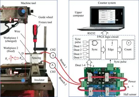
Fig.1 Schematic diagram of experimental device.
3.Discharge characteristics of ultra-fine wire-EDM
The experimental conditions are presented in Table 1.Fig.2 shows the discharge waveforms of molybdenum wires withdiameters of 0.18 mm and 0.05 mm,respectively,during continuous cutting.The waveforms show that the machining process with ∅0.18 mm wire is a single channel discharge.However,there is a certain proportion of multi-channel discharge in the process with ∅0.05 mm ultra-fine wire in addition to the single channel discharge.This section will reveal the multi-channel discharge mechanism of ultra-fine wire from the discharge equivalent model and the electrostatic field between electrodes.

Fig.2 Discharge waveform during continuous cutting.
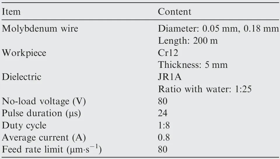
Table 1 Experimental conditions.
3.1.Equivalent circuit model
Aimed at the multi-channel discharge phenomenon in the process of an ultra-fine wire,the equivalent circuit model was established by taking the double channel as an example,as shown in Fig.3.The potential of a conductive block is assumed to be 0 V.C and D are the discharge points.andare equivalent resistances of the discharge channel and dielectric,and ZD is the voltage stabilizing tube.The discharge channels can be approximately equivalent to,,and ZD in the series with Wu et al.is the current limiting resistor of the transistor power supply.Because of the low resistivity of the metal workpiece,it can be regarded as an equipotential body,which is the same as the potential of point A.is the discharge channel maintenance voltage,and theis the voltage between the workpiece and the conductive block.The resistance of the wire electrode increases with the decrease in the wire diameter.The resistance of the 0.18 mm molybdenum wire is approximately 2.2 Ω/m.Its effect on discharge can be ignored.However,the resistance of 0.05 mm molybdenum wire is about 28.5 Ω/m,which can not be ignored compared with that of 0.18 mm electrode wire.There must be a potential difference (-) between the discharge point C and point B.is greater than,and the difference increases linearly toalong the axis of the wire.The equivalent circuits of the single channel discharge and multi-channel discharge are shown in Fig.4.
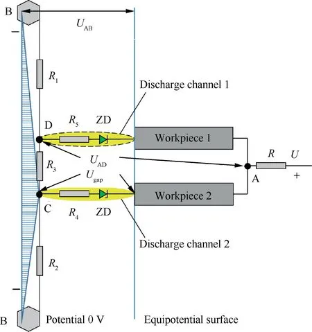
Fig.3 Schematic diagram of gap voltage.
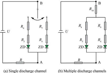
Fig.4 Equivalent circuit model with 0.05 mm.
When only discharge channel 1 exists,the current limiting resistanceadded to the discharge circuit is

When only discharge channel 2 exists,the current limiting resistanceadded to the discharge circuit is

It can be seen from Eqs.(1) and (2) that the effect of the wire resistance on the discharge circuit is affected by the position of the single discharge channel.Because the wire resistance of traditional WEDM can be ignored,the discharge state of a single pulse is almost independent of the thickness of the workpiece.
When the two discharge channels exist at the same time,the equivalent resistanceapplied by the wire electrode to branch 1 is

The equivalent resistanceapplied to branch 2 is

The additional current limiting resistanceis

According to Eqs.(3)-(5),the equivalent resistance distribution of the wire electrode in each branch is related to the spacing between two discharge points.
3.2.Electric field strength between electrodes
Discharge gapis assumed to be 10 μm,and the conductive etching particles are assumed to be a metal ball of 5 μm.To simplify the calculation model,the following assumptions are made:
(1) The influence of the electrode surface morphology on the electric field distribution is neglected.
(2) The gap does not change during the analysis.
(3) The gap electric field is an electrostatic field.
To measure the minimum breakdown voltage of dielectrics between electrodes,the machine tool moves backward 10 μm after tool setting.When the voltage between electrodes is continuously increased,the dielectric in the gap can be broken down to discharge at 70 V.The experimental conditions are shown in Table 1.The results of the distribution of the electric field between electrodes simulated by ANSYS Maxwell are presented in Fig.5.According to Fig.5(b),the maximum dielectric strengthof the dielectric should be less than 9.1044×10V/m.If the resistance of the wire electrode can be ignored,the voltage between electrodes will drop to about 20 V after the dielectric breakdown.Bubbles,carbon particles,and metal particles will cause electric field distortion.The electric field strength with metal particles between electrodes is shown in Fig.5(c).The maximum electric field intensity is 6.9730×10V/m at the E and F ends of the metal particles.The electric field strength is still less than the dielectric strength of the dielectric.Therefore,it is difficult to break down the dielectric to discharge in the traditional WEDM under maintenance voltage.
Furthermore,the resistance of the ultra-fine wire cannot be ignored.Other locations outside the discharge point still have a high potential difference with the workpiece.As shown in Fig.5(d),it is assumed that the potential difference is 27 V.The electric field containing metal particles is 9.4135×10V/m,which exceeds the dielectric strength of the dielectric.Therefore,it is possible to form a discharge in the secondary breakdown dielectric under this voltage.It can be understood from the previous analysis that the larger the spacing between two workpieces and the greater the potential difference,the greater the electric field between electrodes containing metal particles will be.The electric field intensities of 30 V and 35 V are 1.0459×10V/m and 1.2203×10V/m,respectively,as shown in Fig.5(e) and (f).
When the dielectric contains carbon particles or metal particles,their relative permittivity εcan be considered as infinite in the calculation of the electrostatic field because these particles are conductors.The breakdown voltageof the dielectric is about 30 V and can be calculated by Eq.(6).Eq.(6)assumes that the gap electric field is an infinite uniform electric field,and only the influence of the polarization electric field is considered.According to the simulation model in Fig.5(a),
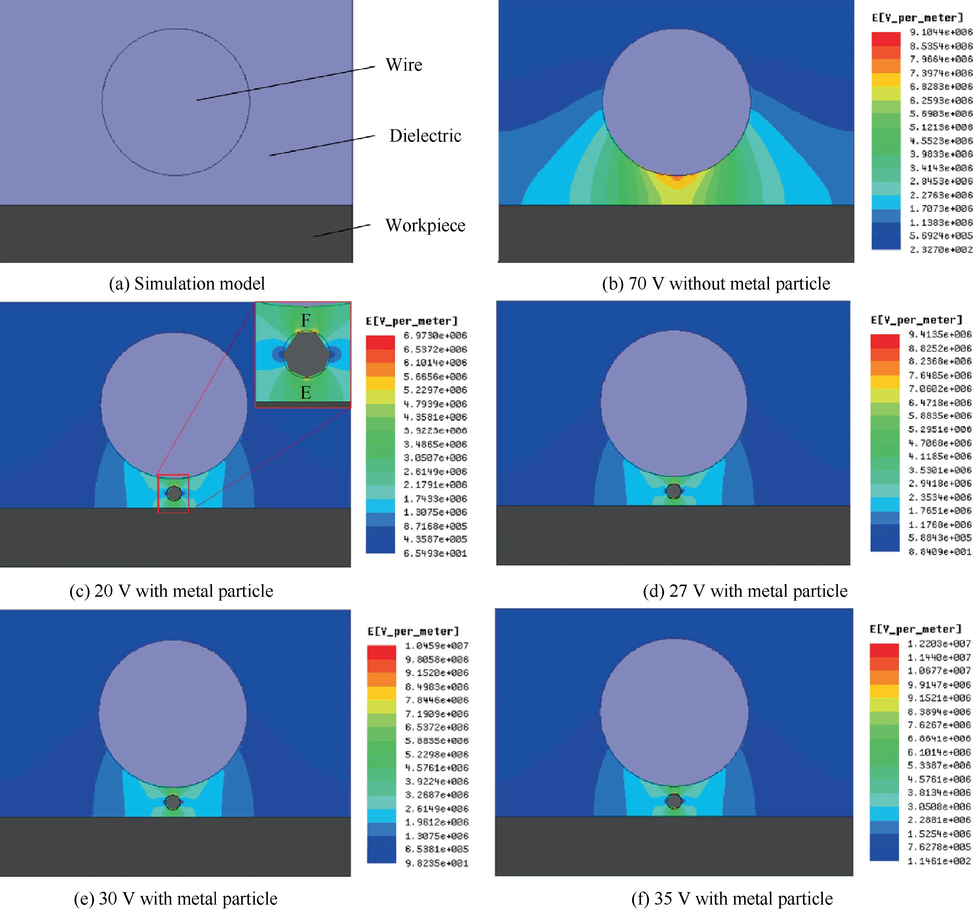
Fig.5 Electrostatic field simulation model and field overlays.
even if the surface morphology of the electrode is ignored,the nearest point between the wire electrode and the workpiece is still equivalent to the tip,so the breakdown voltage is slightly larger than the simulation result.However,both the analytical solution and the simulation results show that the multi-channel discharge may occur when there are conductive particles and have a potential difference higher than the maintenance voltage between the electrodes.

where εis the relative permittivity of dielectric,εis the relative permittivity of particle,is the discharge gap,is the maximum dielectric strength,is the actual required breakdown voltage.
3.3.Multi-channel discharge mechanism
The typical multi-channel discharge waveform is exhibited in Fig.6.The discharge process can be divided into four stages:(1) dielectric breakdown between electrodes and formation of the first discharge channel,(2) establishment of another discharge channel,(3) self-sustained discharge of multiple discharge channels,and (4) multi-channel deionization.The multi-channel discharge mechanism is shown in Fig.7,which corresponds to stages 1-4 in Fig.6.
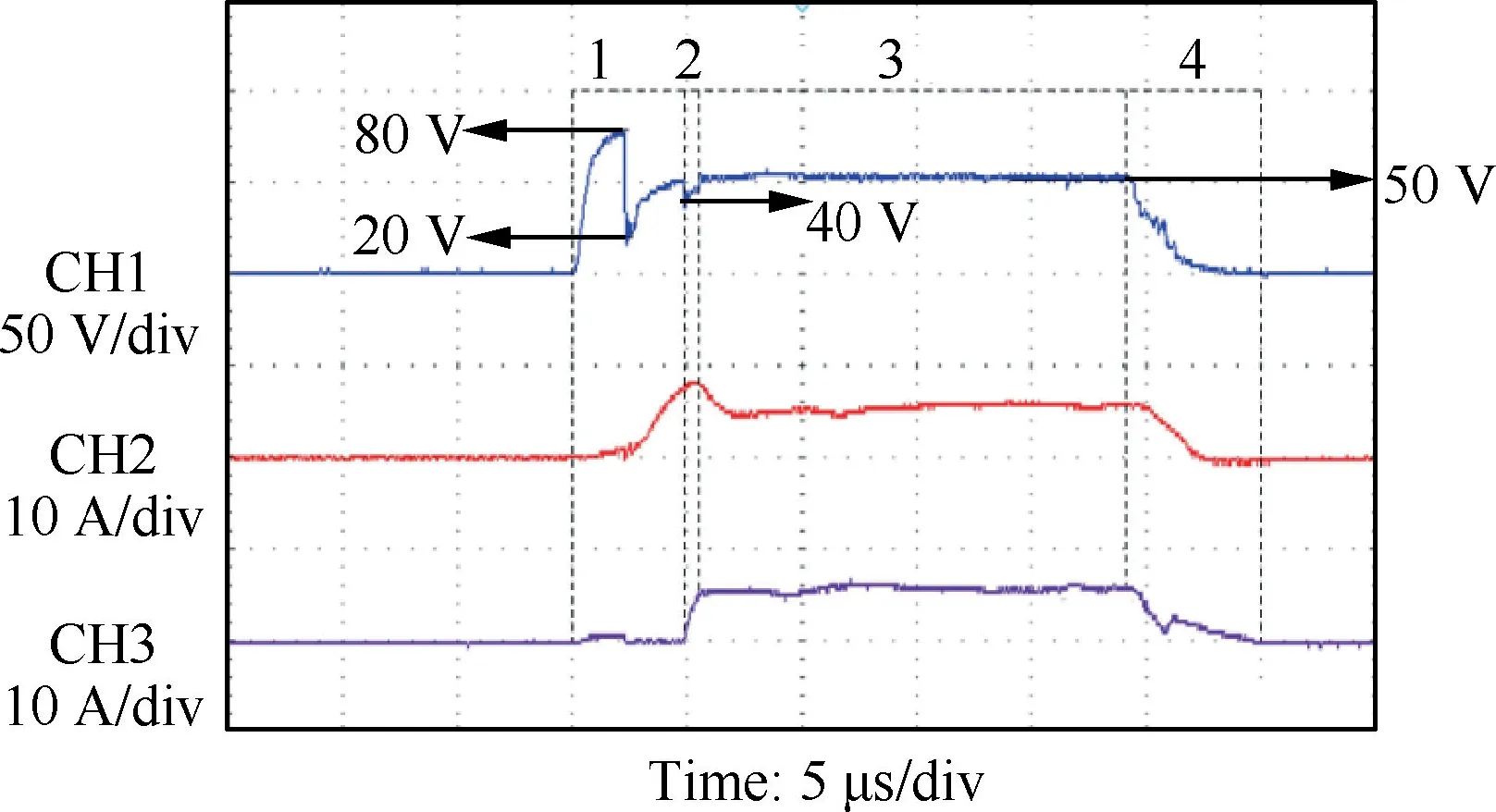
Fig.6 Discharge waveform.
Stage 1:Dielectric breakdown between electrodes and the formation of the first discharge channel,as shown in Fig.7(a).When the pulse voltage is applied between the electrodes,the electric field increases with the decrease in the gap.Once the electric field strength exceeds the dielectric strength of the dielectric,the dielectric will undergo avalanche collision ionization and develop into discharge channel 1.At this time,the inter-electrode voltage decreases from 80 V to about 20 V.With the increase of the current of channel 1,the voltage increases back to about 50 V due to the partial voltage effect of ultra-fine wire resistance.However,there is still a certain potential difference between the electrodes,and the accumulation and chain of conductive particles in the dielectric will further cause the distortion of the electric field between the electrodes.
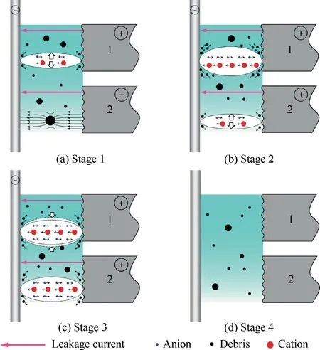
Fig.7 Discharge mechanism in Fig.6.
Stage 2:The establishment of another discharge channel,as shown in Fig.7(b).According to the electric field simulation,the electric field at both ends of the metal particles is the highest.Once the electrostatic field strength exceeds the dielectric strength,the dielectric between the electrodes will be broken down due to the series discharge of particles,which then forms discharge channel 2.At this moment,the two discharge channels coexist.The equivalent resistance of the total circuit decreases because of the parallel connection of the two channels.The circuit of discharge channel 2 is still in the construction stage and the current of discharge channel 2 is still in the rising stage,where the current of discharge channel 1 is slightly increased.Therefore,the voltage between electrodes is reduced from 50 V to 40 V.
Stage 3:Self-sustained discharge of multiple discharge channels,as shown in Fig.7(c).With the formation of discharge channel 2,its current tends to be stable.Although the equivalent resistance of the total circuit decreases,the discharge maintenance voltage remains unchanged at 50 V.The entire discharge system presents a stable self-sustained discharge.
Stage 4:Multi-channel deionization,as shown in Fig.7(d).With the end of the pulse voltage,the self-sustained discharge state is broken.The positive and negative charged particles in the discharge channel are combined into neutral particles,and the dielectric strength is restored.
It can also be seen that,as long as the conditions of dielectric breakdown between electrodes are satisfied,more than two multi-channel discharges can be formed in ultra-fine wire-EDM.
4.Results and discussion
According to the previous analysis,the discharge characteristics of ultra-fine wire are affected by the spatial location of the discharge points.For the convenience of analysis,the thickness of workpieces 1 and 2 is 5 mm,which is far less than the distance of 500 mm between the upper and lower conductive blocks.Ignoring the influence of the thickness on the discharge position,the positions of the two workpieces are approximately the discharge positions.Workpiece 2 was placed on the worktable 200 mm away from the lower conductive block.By changing the spacing between the two workpieces,the variation law of equivalent resistance and multichannel discharge probability was studied.After determining the electrical parameters,the peak current of the discharge pulse was affected by the equivalent resistance of the wire electrode.Then,the change of the peak current affected the erosion ability of the discharge pulse,the surface morphology,the surface roughness,and the thickness of the recast layer.Each experiment was repeated three times,and the average value was taken as the final result to evaluate the cutting efficiency,surface roughness,and recast layer thickness.
4.1.Equivalent resistance of wire electrode
The relationship between the equivalent resistance and the spacing is exhibited in Fig.8.It can be seen from the figure thatfirst increases and then decreases,and reaches the maximum value at 50 mm.This is because the change of position of workpiece 1 results in the change of discharge channel 1 and its discharge point,sois variable during single channel sparking.is determined by the installation position of workpiece 2,and when the spacing is only 100 mm,the two workpieces are symmetrically distributed between the upper and lower conductive blocks,thusandare the same andis equal to.andincrease with the increase of spacing,but the speeds of increase for the two are different.decreases linearly with the increase of spacing.is always slightly larger thanwhen the spacing is less than 100 mm.andare the same when the spacing is 100 mm.However,when the spacing is greater than 100 mm,is greater than,where the difference increases with the increase of spacing.Due to the resistance of the ultra-fine wire cannot be ignored,the distribution of the equivalent resistance is affected by single channel discharge or multi-channel discharge for different thickness machining.
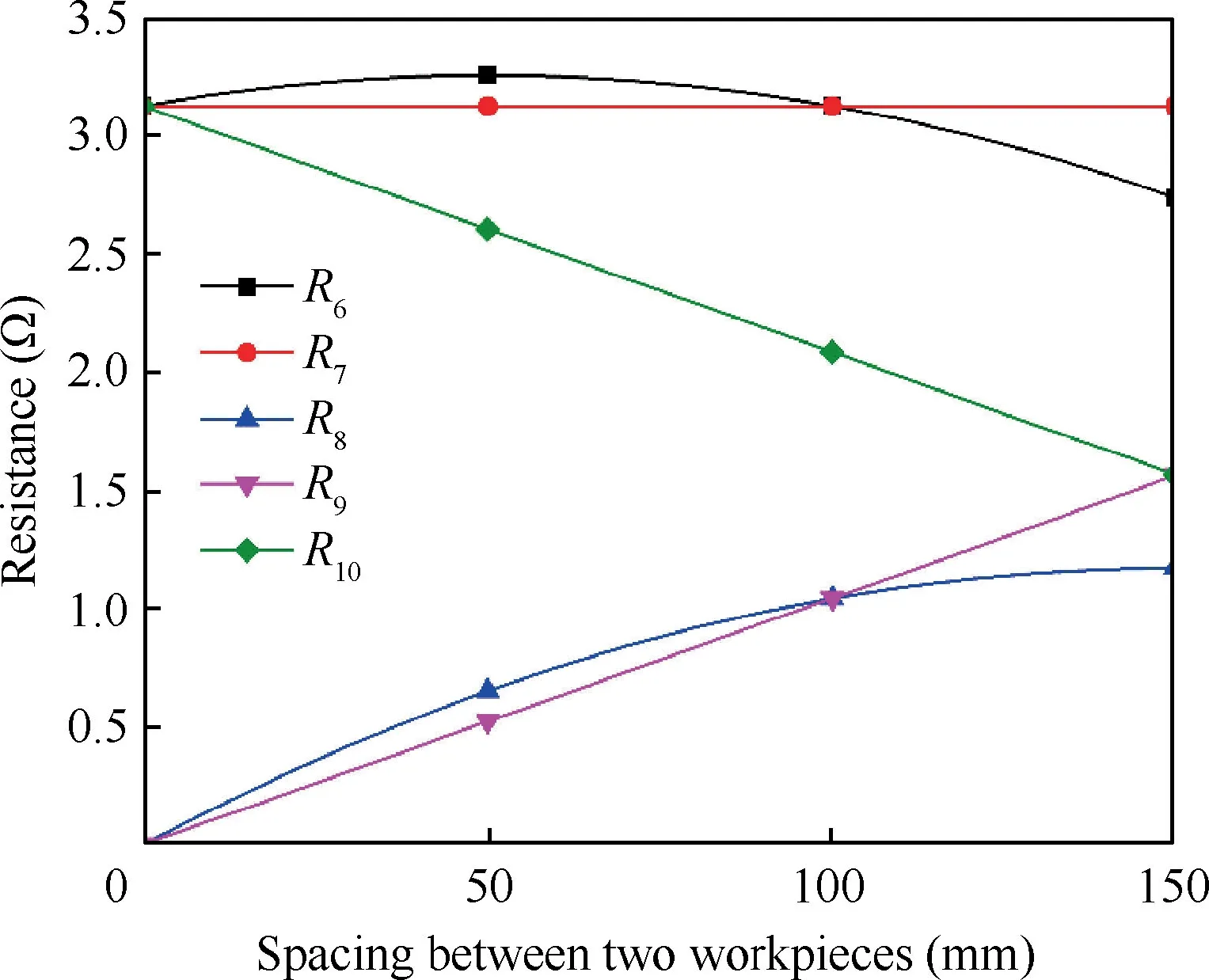
Fig.8 Resistance at different spacings.
4.2.Discharge waveform between electrodes
The distributions of electric potential and equivalent resistance of ultra-fine wire are affected by the spacing between two workpieces.To further analyze its influence on machining,the discharge waveforms of 50 mm,100 mm,and 150 mm were intercepted by an oscilloscope.The experimental parameters are shown in Table 1.It can be seen from Fig.9 (a)-(c) that after a breakdown delay of about 2 μs,the dielectric is broken down and a discharge channel is generated.decreases rapidly from 80 V to approximately 20 V if the wire resistance was ignored.That is,the maintenance voltage was about 20 V.However,the resistance of an ultra-fine wire cannot be ignored,so the voltage between electrodes increases with the increase of current,and acts together with current limiting resistance to maintain self-sustained discharge.For the three different spacings,the values ofare all greater than 20 V.Furthermore,at the same spacing,the difference inis 10 V when discharging separately because of the difference ofand,as shown in Fig.9(d).The change of equivalent resistance of wire electrode affects the discharge voltage between electrodes.
According to the current waveform in Fig.9,the peak current of branch 1 (discharge channel 1) increases with the increase of spacing,while the peak current of branch 2 (discharge channel 2) decreases with the increase of spacing.Becauseandare the same,the peak current of the two discharge channels is the same at a spacing of 100 mm,which is 6 A,as shown in Fig.9(b).Compared with Fig.9(a)and(c),the peak current of the two branches is different with different spacing,but the difference is greater at a spacing of 150 mm.The variation law of peak current is consistent with that of resistance in Fig.8.Although the peak current of each branch is different,it is smaller than that of a single spark discharge.This indicates that the multi-channel phenomenon of ultra-fine wire has the characteristic of dispersing energy,as shown in Fig.10.The multi-channel discharge affects the discharge voltage and current in the thickness direction.
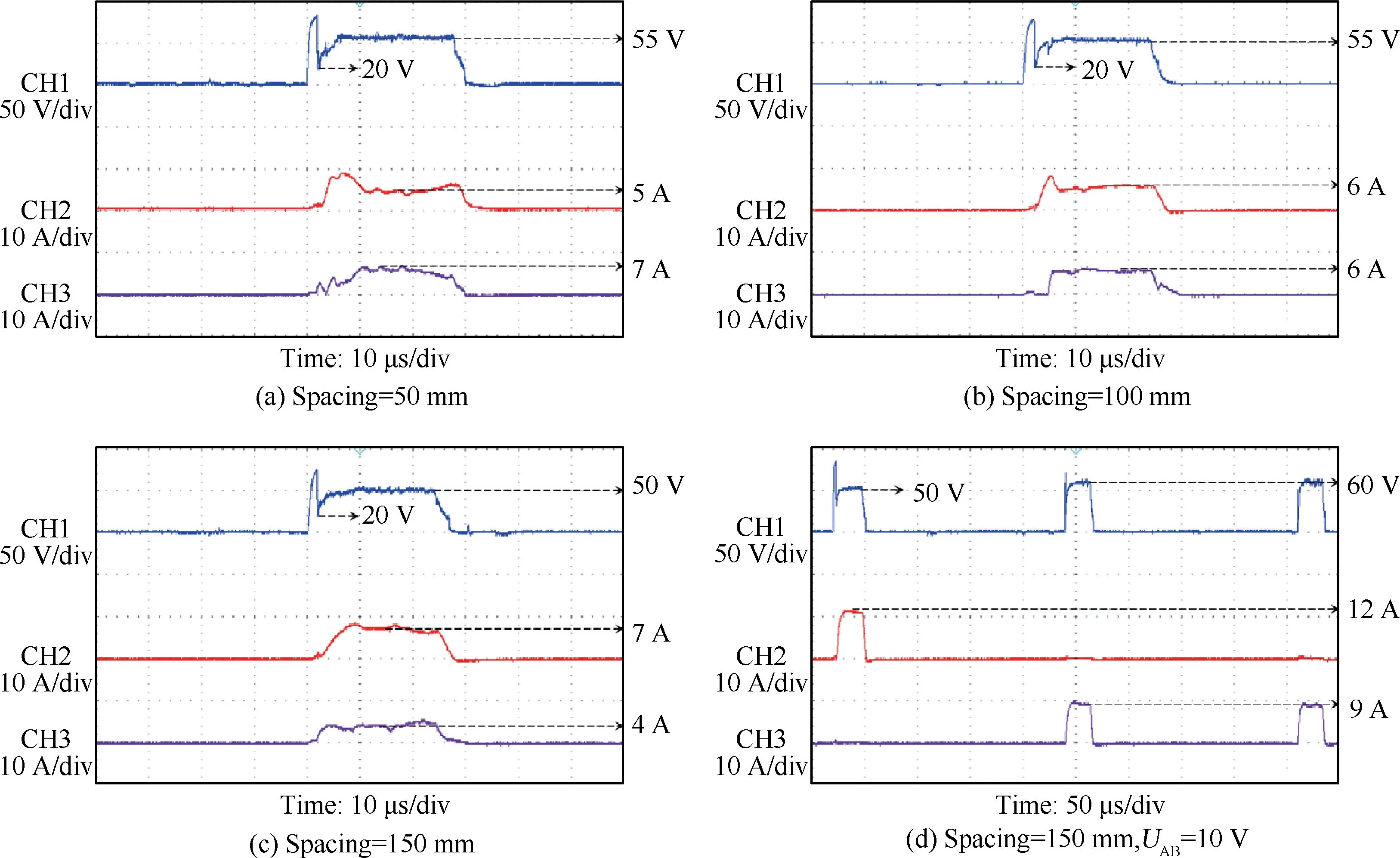
Fig.9 Discharge waveform at different spacings.
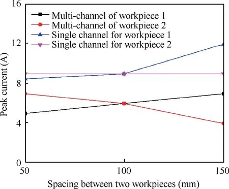
Fig.10 Peak current at different spacings.
4.3.Influence of spacing on multi-channel discharge probability
Using the experimental parameters in Table 1,the relationship between(discharge numbers of workpiece 1) and N(discharge numbers of workpiece 2) and spacing is shown in Fig.11.It can be seen from the figure that the ratio of(discharge numbers of multi-channel)toandtoincreases with the increase of the spacing between two workpieces,but the growth rate ofis slightly faster than that of.At a spacing of 100 mm,the two workpieces are symmetrically distributed,and the equivalent resistance of wire electrode is the same.The peak current of the single discharge and multichannel discharge are the same,so the machining speed of the two workpieces is almost the same.In other words,the discharge numbers of the two workpieces are almost the same.In the range of 50 mm to 100 mm,the peak current of workpiece 1 is larger than that of workpiece 2,and the volume of the single effective discharge pulse is larger.For the same material removal volume,workpiece 1 requires less effective discharge pulses,sois less than.However,processing condition above 100 mm is the opposite.Because the differences between,,,andincrease faster than that of spacing less than 100 mm,workpiece 2 at a spacing of 150 mm requires a more effective discharge pulse to achieve the same material removal volume.Moreover,anddecrease faster.After the discharge of workpiece 1,does not noticeably change with the spacing increase,so the number of multi-channel discharges at 150 mm is not directly proportional to the spacing.Due to the influence of spacing on the equivalent resistance and discharge frequency,the machining efficiency of 50 mm,100 mm,and 150 mm is respectively increased by 7.2%,8.7%,and 15.6% compared with the 0 mm spacing,as shown in Fig.12.
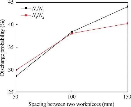
Fig.11 Multi-channel discharge probability.
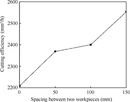
Fig.12 Cutting efficiency.
4.4.Surface topography
The surface morphology and three-dimensional morphology of the two workpieces at different spacings are shown in Fig.13.It can be seen from the figure that the surfaces machined with different spacings have the typical characteristics of discharge crater accumulation and spherical droplet in WEDM.At a spacing of 0 mm,the discharge between electrodes is basically single channel discharge,and the discharge crater is large.The surface roughnessis 4.005 μm,as shown in Fig.13(a)and(b).As the discharge probability of the multichannel increases with the spacing increase,it exhibits the characteristics of energy dispersion;the crater is small,so the surface is relatively flat,as shown in Fig.13(c) and (e).Compared with the 0 mm spacing,the surface roughnessat 100 mm decreases by 37.7%.However,as the peak current difference between the multi-channel and single spark discharge of workpiece 2 increases with the spacing increase,the surface roughnessat 150 mm increases slightly compared with that at the 100 mm spacing,as shown in Fig.13(f).However,at 150 mm spacing,the peak current of the single spark discharge and the multi-channel of workpiece 1 is greater than that of workpiece 2.Therefore,the craters are characterized by larger small craters and larger large craters.The surface roughness Ra is larger (3.404 μm),but it is still less than the surface roughness at the 0 mm spacing.
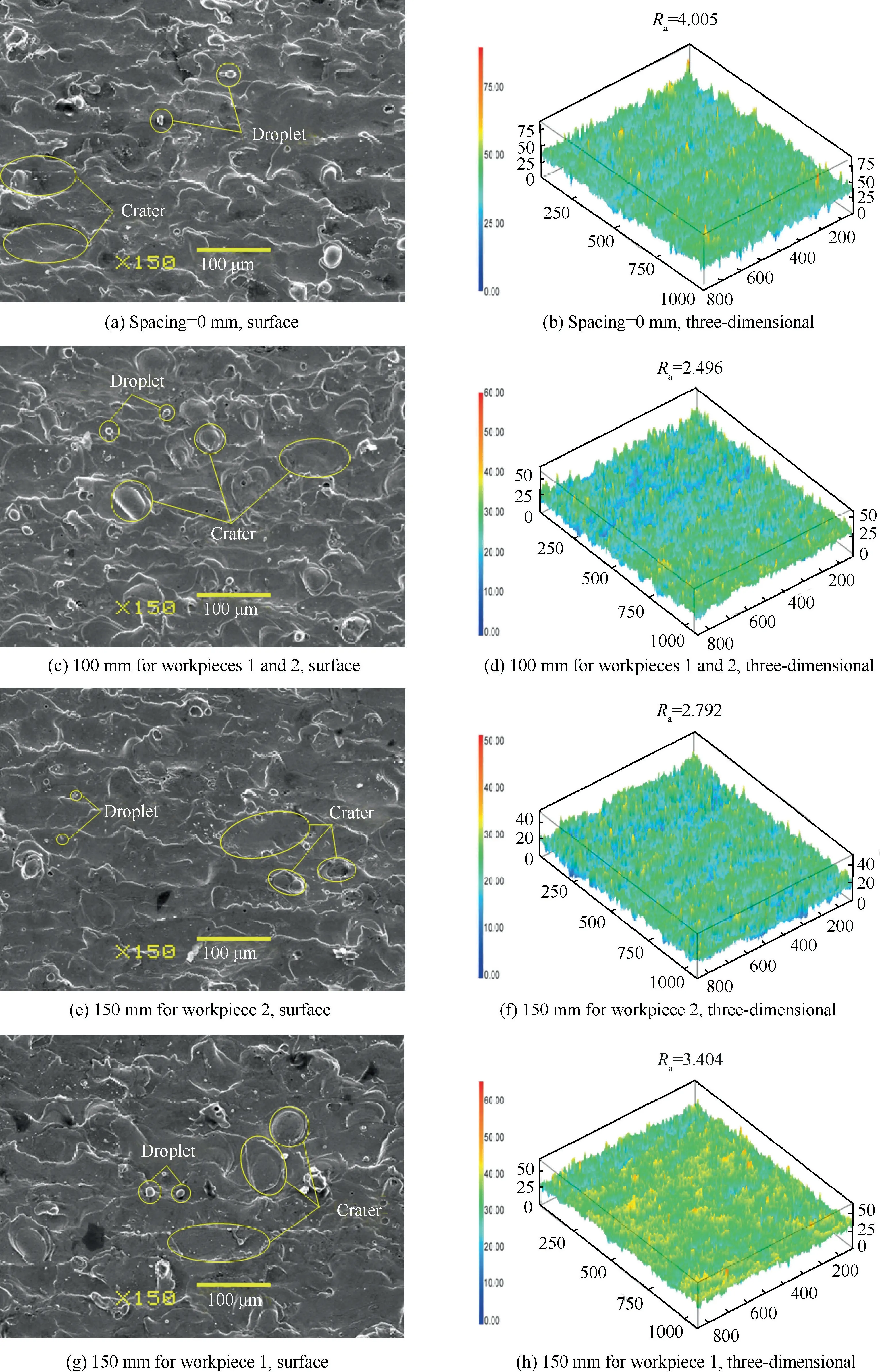
Fig.13 Surface morphology and three-dimensional profile at different spacings.
4.5.Recast layer
The cross-sectional recast layer is shown in Fig.14 at four different spacings.The thickness of the recast layer is not uniform because of the time and spatial randomness of the spark discharge.Combined with the equivalent resistance and discharge waveform of the wire electrode,the peak current of the two workpieces at a spacing of 0 mm and 100 mm are the same,so the surface characteristics after machining are almost the same,as shown in Fig.14(a) and (b).The peak current of the single spark discharge of workpiece 2 is 9 A,which does not change with the spacing.The maximum thickness of the recast layer is about 16 μm.At a spacing of 150 mm,the peak current of the single spark discharge of workpiece 1 increases to 12 A,so the maximum thickness of the recast layer increases to 19 μm,as shown in Fig.14(f).For workpiece 2,with the increase of spacing,the material removal tends to present high frequency and small volume,so the average recast layer thickness gradually decreases,as shown in Fig.14(a),(b) and (e).However,for workpiece 1,the probability of a multi-channel discharge and the peak current increases with the increase of spacing.The material removal tends to be high frequency and large volume,so the average thickness of the recast layer gradually increases,as exhibited in Fig.14(a),(b),and (f).The metallographic photos of two workpieces at a spacing of 100 mm are shown in Fig.14(c) and Fig.14(d) respectively with a measurement length of 705 μm.The maximum recast layer thickness in this length range does not exceed 9 μm.The thickness of recast layer shown in Fig.14(a),(b),(e) and(f) under corresponding spacing is representative.The thickness of the recast layer in the thickness direction is affected by multi-channel discharge,even if the processing conditions are the same.
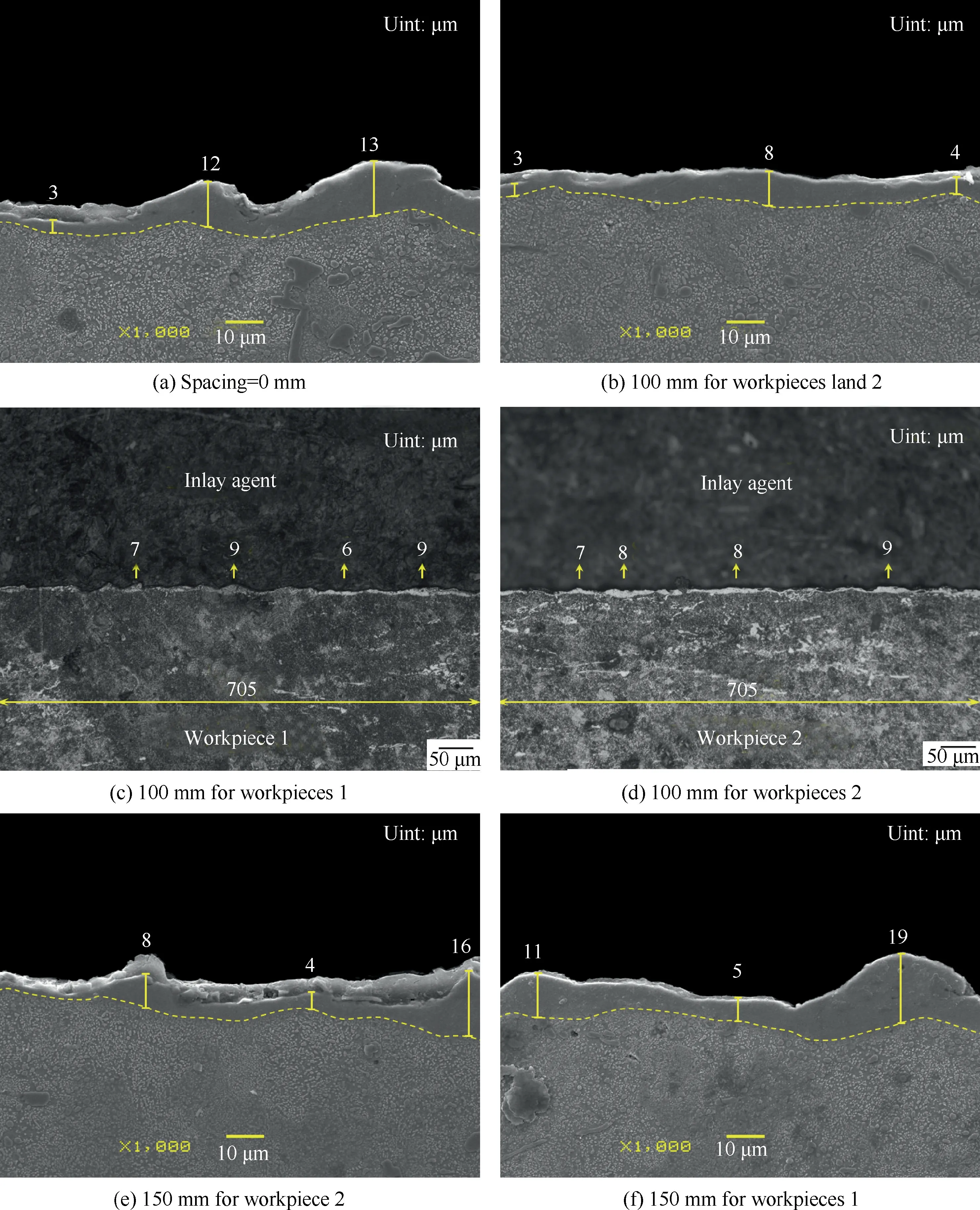
Fig.14 Cross-sectional recast layer at different spacings.
5.Conclusions
Based on the analysis of the equivalent discharge model and the electrostatic field between electrodes,it was found that multi-channel discharge exists in ultra-fine wire-EDM.The number of multi-channel discharges with different distances between the two workpieces is counted by the designed device.The conclusion is as follows:
(1) There is still a certain potential difference outside the discharge point and it increases linearly along the wire axis machined by the ultra-fine wire.The distribution of the electrostatic field between electrodes can be changed by conductive particles in the dielectric.The multichannel discharge probability increases with the increase of workpiece thickness.
(2) Multi channel discharge phenomenon affects the peak current and discharge frequency for different workpiece thickness machining.The distributions of the equivalent resistance and the peak current of the wire electrode are affected by the position of the single spark and the multi-channel discharge.With the increase of the multi-channel probability,the number of discharges in each workpiece increases,so the machining efficiency can be improved to a certain extent.Compared with the 0-mm spacing,the machining efficiency at 100 mm and 150 mm increased by 8.7%and 15.6%,respectively.
(3) The energy dispersion of the multi-channel discharge can reduce the surface roughness Ra and the thickness of the recast layer to a certain extent.The surface roughness Ra and the average recasting thickness under a spacing of 100 mm decreased by 37.7%and 46.6%compared with the 0 mm spacing,respectively.This indicates that the installation position affects the discharge energy of single channel and multi-channel during ultra-fine wire cutting.In practical machining,the workpiece should be in the symmetrical position between two conductive blocks as far as possible(for example,under the condition of this paper,the spacing of 100 mm is the symmetrical position).By adjusting the position of the workpiece,better processing index can be obtained under the same processing conditions.
(4) The thickness of recast layer in the thickness direction is affected by multi-channel discharge.Under the experimental conditions,the average thickness of recast layer is 5 μm and uniform at 100 mm spacing.
The authors declare that they have no known competing financial interests or personal relationships that could have appeared to influence the work reported in this paper.
This work was co-supported by the National Natural Science Foundation of China (Nos.51575271 and 51975290).
 Chinese Journal of Aeronautics2022年2期
- Chinese Journal of Aeronautics的其它文章
- Pressure-induced instability and its coupled aeroelasticity of inflated pillow
- Adjoint boundary sensitivity method to assess the effect of nonuniform boundary conditions
- Transit time difference and equal or non-equal transit time theory for airfoils with lift
- A boundary surrogate model for micro/nano grooved surface structure applied in turbulence flow control over airfoil
- Nonlinear uncertainty quantification of the impact of geometric variability on compressor performance using an adjoint method
- High precision and efficiency robotic milling of complex parts:Challenges,approaches and trends
