吲哚方酸菁半导体在场效应晶体管中的应用
2011-12-11 09:08孙秋健董桂芳郑海洋赵昊岩炼王立铎张复实
物理化学学报 2011年8期
孙秋健 董桂芳 郑海洋 赵昊岩 乔 娟 段 炼王立铎 张复实 邱 勇
(有机光电子与分子工程教育部重点实验室,清华大学化学系,北京100084)
吲哚方酸菁半导体在场效应晶体管中的应用
孙秋健 董桂芳*郑海洋 赵昊岩 乔 娟 段 炼王立铎 张复实 邱 勇*
(有机光电子与分子工程教育部重点实验室,清华大学化学系,北京100084)
研究了2,3,3-三甲基-1-H-吲哚方酸菁的场效应性质,通过X射线衍射证实了方酸菁分子内电荷分离结构以及分子间面面堆积模式,并在Si/SiO2基片上通过真空蒸镀和旋涂的方法制备了p型晶体管器件.通过对器件性能与沟道形态的研究,我们发现退火处理能促进方酸菁薄膜由无定形态向多晶态转变,从而使薄膜晶体管的迁移率从10-5cm2·V-1·s-1量级提高到10-3cm2·V-1·s-1量级.顶接触结构单晶器件获得了7.8×10-2cm2·V-1·s-1的迁移率.未封装的方酸菁晶体管在大气中也表现出较好的稳定性.
方酸菁内盐;有机晶体管;旋涂;单晶;退火
1 Introduction
Organic semiconductors are the most important element in organic thin-film field-effect transistors(OTFTs).1-4Both experimental results and theoretical calculations have verified that the current magnification of gate bias in OTFTs results from the hopping process of field induced carriers between adjacent molecules,and thus close packing of the molecules can improve charge transport through the overlapping frontier orbital.5-8Hitherto,lots of π-conjugated organic small molecules and polymers with small energy gaps,such as pentacene,9-11copper phthalocyanine(CuPc),12-14perylene diimide,15oligothiophene,16,17and their derivatives,18,19have been investigated to realize high mobility.Since the initial status of these organic films by traditional processing techniques is usually less ordered,uniform and oriented polycrystallization of the film,especially at the first few layers near the semiconductor/dielec-tric interface,is the key to improve the performance of OTFTs. Thus post-processing such as annealing is frequently used to improve the microstructure of the semiconductor layer.20
In order to facilitate the thermodynamic phase transition during annealing,squarylium inner salt,a kind of compounds with strong intendancy of self crystallization,was focused as the semiconductor in OTFTs.Though squarylium dyes have been widely used as photoconductors in printers and organic solar cells due to their fine stability and transport property,21,22they are less reported in organic transistors.23-25In this paper,1,3-bis [(3,3-dimethylindolin-2-ylidene)methyl]squaraine(ISQ,Fig.1 (a))was studied in both thermal vacuum deposited and solution processed transistors.This molecule is nearly planar and has a fine π-π packing along b direction in crystal phase(Fig.1 (b)),which is expected to benefit the field effect transport.
2 Experimental
2.1 Material synthesis
ISQ was synthesized by a modified procedure according to reference.263,4-dihydroxy-3-cyclobutene-1,2-dione(99%)and octadecyltrichlorosilane(OTS,95%)were purchased from Acros.The 2,3,3-trimethyiindolenine(97%)was purchased from Alfa Aesar.The other chemicals and solvents were purchased from Sigma-Aldrich.All the chemicals were analytically pure and used as received without further purification unless otherwise stated.3,4-Dihydroxy-3-cyclobutene-1,2-dione and 2,3, 3-trimethyiindolenine in stoichiometric ratio were heated in refluxing mixture of toluene and n-butanol for 6 h.The byproduct,water,was removed azeotropically using a Dean-Stark trap.The precipitate was rinsed with petrol ether.Then it was sequently purified by column chromatography and recrystallization to get gold-shine needle-like crystals with a yield of 85%.The purity was assessed to be about 99.5%by high performance liquid chromatography(Agilent 1100,USA).
2.2 X-ray crystallography
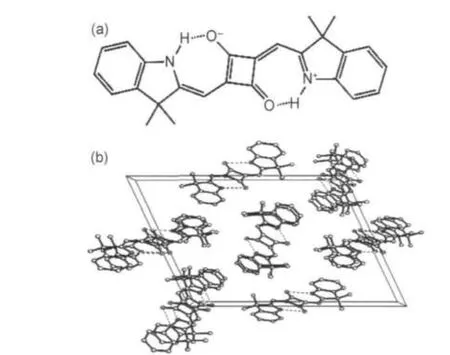
Fig.1 (a)Chemical structure of ISQ and(b)its crystal packing along b direction
A prism-shaped single crystal was grown by slow evaporation of the ISQ/dichloromethane solution at room temperature. Structural X-ray diffraction was performed on a CCD diffractometer(BrukerAPEX,Germany)equipped with graphite monchromatized Mo Kαradiation.Details of crystal parameters,data collection,and structure refinement are given in Table 1.Data collection was controlled by SMART program(Bruker, 1997).Computations were performed using the SHELXTL NT ver.5.10 program package(Bruker,1997)on an IBM PC 586 computer.Analytic expressions of atomic scattering factors were employed,and anomalous dispersion corrections were incorporated(International Tables for X-ray Crystallography, 1989).Crystal drawings were produced with XP(Bruker, 1998).
2.3 Photochemical and electrochemical properties
The ISQ film was deposited on a quartz glass from methanol solution.The absorption was recorded with a UV-Vis spectrophotometer(Agilent 8453,USA).The fluorescence emission was recorded with a uoro-spectrophotometer(Jobin Yvon Fluro Max-3,France).The maximum absorption and emission were observed at 644 and 664 nm respectively,with nearly symmetric shapes(Fig.2).From the absorption edge,the band gap of ISQ was calculated to be 1.83 eV.
The electrochemical properties of ISQ were investigated by cyclic voltammetry.The measurement was performed on a voltammetric analyzer(Princeton Applied Research Potentiostat/Galvanostat model 283,USA)in dichloromethane at a scan rate of 100 mV·s-1.Ferrocene was added in as an internalreference.The oxidation potentials were 0.971 V for ISQ and 0.528 V for ferrocene(Fig.3).The highest occupied molecular orbital(HOMO)of ISQ was then calculated to be-5.24 eV versus vacuum.According to the spectrum data,the lowest unoccupied molecular orbital(LUMO)of ISQ was deduced to be-3.41 eV.

Table 1 Data collection,processing and structure refinement for the structural X-ray diffraction of ISQ

Fig.2 UV-Vis absorption and photoluminescence spectrum of ISQ film
2.4 Fabrication of transistors
Field-effect transistors were fabricated in a bottom-gate, top-contact architecture with a highly n-doped silicon wafer as the gate electrode and 300 nm thermally grown SiO2as the gate dielectric.The substrates were cleaned by sonication in organic solvents.Then the SiO2surface was treated in piranha solution and modified with OTS.ISQ was deposited onto the SiO2substrate at a rate of 1 nm·s-1under 10-4Pa.For solution process,the ISQ semiconductor was spin-coated from a 4 g·L-11,2-dichloroethane solution and then baked on a hot plate at 80°C in N2atmosphere.The thickness of ISQ thin film was controlled at 45 nm.For crystal transistors,the crystal strips were in-situ assembled on OTS modified Si/SiO2substrate by immersing the substrate into an ISQ/dichloromethane solution (10-3mol·L-1)and then slowly evaporating the solution in a saturated hexane atmosphere for two weeks.Finally,the source and drain contacts were formed by thermal vacuum deposition of Au thin film through shadow masks.Electrical characterization of the transistors was performed in air without encapsulation with a semiconductor characterization system(Keithley SCS 4200,USA).
2.5 Surface morphology

Fig.3 Cyclic voltammetry of ISQ with ferrocene included
The dynamic atomic force microscopy(DAFM)of the ISQ film was taken by a scanning probe microscope(Seiko SPI 3800 Series SPA-400,Japan).The optical images of the thin films,the crystal strips,and the top view of the transistors were recorded with a microscope(Olympus BX51M,Japan).
3 Results and discussion
The classical structure of ISQ is shown in Fig.1(a).Because of the isomerous effect of squaric acid,opposite charges are located in oxygen and nitrogen atoms separately.A near flat configuration of ISQ is kept with only 7°distortion in the crystal, according to the crystal packing data(Fig.1(b)).The optimized structure was given by geometrical optimization with Gaussian98 at B3LYP/6-311+G(d,p)level(Fig.4).Symmetrical frontier orbital is delocalized among the whole molecule for both HOMO and LUMO due to the fast resonance with charge exchange.
The electron density contour map in the molecular plane was calculated by“EDEN”command of Shelxtl XP program (Fig.5).FoFourier method was chosen to process the crystal diffractional data.By counting the electron numbers per each carbon atom,it is found that the electron density decreases from the central part to the side groups.In order to clarify the transport property of ISQ,the inner reorganization energy was calculated based on the result of static energy and geometry optimization for positive and negative ISQ ions at B3LYP/6-311+ G(d,p)level.The reorganization energy was 0.168 and 0.271 eV for hole and electron,respectively.The relatively smaller value for hole carriers suggests that ISQ is mainly a p-type transporter.
According to thermal gravity analysis,mass loss of ISQ occurred at 287.8°C.The attached methyls also enable ISQ to solve in most halohydrocarbon.Thus,ISQ thin films could be prepared by both thermal evaporation and solution process. The morphology of films was characterized by dynamic atomic force microscopy(DAFM)(Fig.6).The root mean square roughness(RRMS)was generally less than 0.5 nm.
Top contact bottom gate architecture was employed in ISQ transistors(Fig.7).Since the HOMO of ISQ are-5.24 eV,gold was used as the source and drain electrodes to achieve energy level matching.As expected before,ISQ TFTs performed hole-transport properties with saturated output curves.However,the initial mobility of vacuum evaporated and spin-coated devices ranged from 10-6to 10-5cm2·V-1·s-1with a low on/off current ratio.

Fig.4 HOMO and LUMO of the singlet ground-state ISQ

Fig.5 Contour map of crystal electron density in the molecular plane

Fig.6 DAFM morphologies in the area of 5 μm×5 μm of(a)thermal evaporation film,(b)spin coated film from C2H4Cl2and(c)single crystal strip on SiO2substrate
In order to accelerate the polycrystallization of the semiconducting layer,the devices were then annealed in the N2-filled glove box at 80°C for 8 h.As a result,crystal-like patterns were observed on the surface of the semiconductor layer,and the mobility increased to 10-4-10-3cm2·V-1·s-1,about two orders of magnitudes higher than initial devices.To explore the structure of the annealed film,X-ray diffraction was applied with a diffractometer(Rigaku-2500,Japan)equipped with a Cu target.2θ scan ranged from 3°to 100°at a speed of 6(°)·min-1. The diffraction pattern proved the presence of polycrystalline phase(Fig.8).The major electrical parameters of various transistors were summarized in Table 2.For each kind of transistors,the data were averaged for effective channels in a batch of 11 devices.Transfer and output characteristics of the best device were shown in Fig.9.The on/off ratio was defined as the current of-120 V over that of 30 V in transfer curves.

Fig.7 Architecture of the ISQ thin film transistor
Generally,the performance of ISQ transistors was enhanced by both OTS modification and annealing.However,the effect of annealing was largely dependent on channel morphology.In about 40%of the spin coated devices,ISQ film aggregated into irregular polycrystalline particles(Fig.10(c)).The amplified inset shows the microscopic film continuity is completely destroyed,which resulted in noneffective devices.In rest devices, although channel smoothness was somewhat decreased,the polycrystalline film still kept connectivity between source and drain electrodes(Fig.10(b)).In this case,the improvement of performance further proves the mobility and on/off ratio of polycrystalline film is higher than amorphous one.For vacuum evaporation,the percentage of noneffective devices resulting from the channel discontinuity was 5%.The difference in success rate indicates the residual solvent in solution processed film facilitated excessive crystallization in annealing,and induced larger polycrystalline particles and rougher surface. Therefore annealing condition needs to be properly controlled to improve the quality of the semiconductor layer.

Fig.8 X-ray diffraction patterns of 200 nm ISQ film after annealing
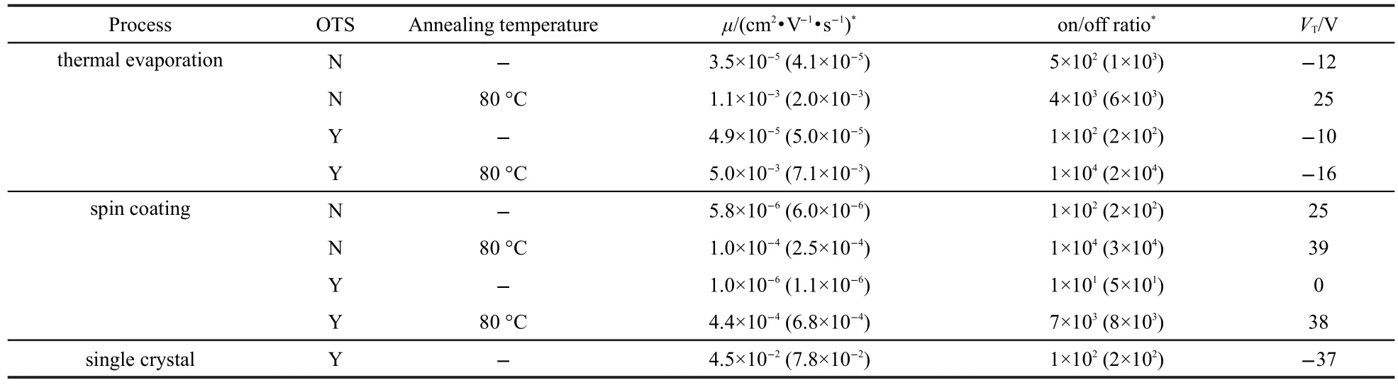
Table 2 Electrical characterization of various ISQ transistors

Fig.9 Transfer and output curves of ISQ thin-film transistors by(a,b)thermal evaporation and(c,d)spin coating with a W/Lof 20Idrain:drain current,Vdrain:drain voltage,Vgate:gate voltage

Fig.10 Channel images of spin coated ISQ film(a)before annealing,(b)enhanced device after annealing, (c)noneffective device after annealing
Since the mobility of ISQ thin film transistors is not as high as ordinary organic semiconductors,further optimization is necessary.Firstly,the interaction between the dielectric surface and the organic semiconductor affects the assembly of the initial ISQ layers,so the selection and modification of dielectric are important.Secondly,as the crystallinity and crystal orientation were uncontrolled in present process,inducing ordered packing along the channel is expected to greatly improve the performance.Thereby ISQ single crystal was evaluated on Si/ SiO2substrate.Fig.11 illustrates the process of the crystal deposition by diffusion of good and poor solvents.OTS-modified Si/SiO2substrate was firstly immersed into the ISQ/dichloromethane solution of 1×10⁻³mol·L-1and then the solvent was evaporated slowly in a saturated hexane atmosphere for two weeks.The precipitation of single crystal strips was found to adhere to the SiO2surface.Extra crystal precipitation was rinsed from the substrate by hexane.100 nm gold was deposited onto the crystal strips as source and drain electrodes.Fig.12 (a,b)is the top view of channel in the crystal transistor.Fig.12 (c,d)shows the characteristic curves of the crystal transistor. The highest mobility,the corresponding on/off ratio,and threshold voltage were calculated to be 7.8×10⁻²cm2·V-1·s-1, 102,and-37 V,respectively.
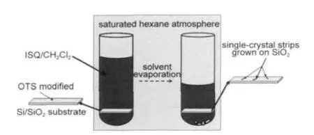
Fig.11 Illustration of the growth of ISQ single crystal on Si/SiO2substrate
In comparison to thin films,the mobility of ISQ single crystal increased by only 10×,but the on/off ratio decreased by 100×and threshold voltage increased.It was noteworthy that the thickness of the crystal strips was about 30 μm while the filed effect thickness was normally less than 10 nm.For bottom gate top contact structure,large thickness shields the function of gate electric field and brings high threshold voltage. The extra thickness had negligible contribution to the on-current but greatly affected the off-current.In an approximate analysis,the channel along direction of thickness could be treated as parallel connection between source and drain.Therefore compared to a crystal strip with 30 nm-thickness,the off-current would increase 1000×and result in a 3-magnitude drop of on/off ratio.Thinner crystal strip and bottom contact structure are promising to solve these problems.
The stability of OTS treated ISQ transistors after annealing was also investigated(Fig.13).The devices were stored in air without encapsulation and measured each month.Six months later,no obvious break down was observed for single crystal and spin-coated devices.The mobility value of thermal vacuum deposition device decayed about 70%at first few months and became relatively stable for the rest time.As H2O and O2traps in the channel were thought to be the predominant physical reasons for the degradation of OTFT in ambient.27This result suggests that the crystal phase with compact structure may serve as a passivation layer and effectively prevents the permeation of H2O and O2from ambient.

Fig.12 (a)Top view of the ISQ single crystal transistor,(b)self-assembled single crystal strips and source drain electrodes on the substrate, (c)output and(d)transfer curves of the ISQ single crystal transistor with a W/Lof 2

Fig.13 Stability of ISQ transistors in air
4 Conclusions
In summary,this work explored the potentiality of a flat structured organic inner salt,ISQ,as semiconductor in field-effect transistor via thermal evaporation and solution process. The performance improvement via post annealing was found to be associated with the spontaneous crystallization process of ISQ film.Single crystal of ISQ was also self-assembled on Si/ SiO2substrate.The highest mobility of 7.8×10⁻²cm2·V-1·s-1was achieved without optimization.This research indicated that 1,3-substituted squarine is a promising field-effect material and the performance may be further improved via more effective molecular design.
Acknowledgement: The authors greatly appreciate the help from Professor WANG Ru-Ji and Dr.LI Zhong-Yu in the analysis of crystal structure and synthesis.
(1) Horowitz,G.Adv.Mater.1998,10,365.
(2) Bao,Z.N.;Lovinger,A.J.Chem.Mater.1999,11,2607.
(3) Dimitrakopoulos,C.D.;Mascaro,D.J.IBM J.Res.Dev.2001, 45,11.
(4) Forrest,S.R.Nature 2004,428,911.
(5)Koren,A.B.;Curtis,M.D.;Francis,A.H.;Kampf,J.W.J.Am. Chem.Soc.2003,125,5040.
(6) Bredas,J.L.;Calbert,J.P.;da Silva,D.A.;Cornil,J.Proc.Natl. Acad.Sci.U.S.A.2002,99,5804.
(7) Choi,H.Y.;Kim,S.H.;Jang,J.Adv.Mater.2004,8,732.
(8) Lan,L.F.;Peng,J.B.;Sun,M.L.;Zhou,J.L.;Zou,J.H.; Wang,J.;Cao,Y.Organ.Electr.2009,10,346.
(9) Virkar,A.;Mannsfeld,S.;Oh,J.H.;Toney,M.F.;Tan,Y.H.; Liu,G.Y.;Scott,C.;Miller,R.;Bao,Z.N.Adv.Func.Mater. 2009,19,1962.
(10) Liang,Y.;Dong,G.F.;Hu,Y.;Wang,L.D.;Qiu,Y.Appl.Phys. Lett.2005,86,132101.
(11) Gundlach,D.J.;Lin,Y.Y.;Jackson,T.N.;Nelson,S.F.; Schlom,D.G.IEEE Electron Device Lett.1997,18,87.
(12)Wang,J.;Wang,H.B.;Yan,S.J.;Huang,H.H.;Yan,D.H. Appl.Phys.Lett.2005,87,093507.
(13)Wu,W.P.;Zhang,H.L.;Wang,Y.;Ye,S.H.;Guo,Y.L.;Di,C. G.;Yu,G.;Zhu,D.B.;Liu,Y.Q.Adv.Funct.Mater.2008,18, 2593.
(14)Zhang,J.;Wang,H.B.;Yan,X.J.;Wang,J.;Shi,J.W.;Yan,D. H.Adv.Mater.2005,17,1191.
(15) Cai,X.;Qi,D.D.;Zhang,Y.X.;Bian,Y.Z.;Jiang,J.Z.Acta Phys.-Chim.Sin.2010,26,1059.[蔡 雪,齐冬冬,张跃兴,边永忠,姜建壮.物理化学学报,2010,26,1059.]
(16) Ie,Y.;Nitani,M.;Tada,H.;Aso,Y.Organ.Electr.2010,11, 1740.
(17)Ahmed,M.O.;Wang,C.M.;Keg,P.;Pisula,W.;Lam,Y.M.; Ong,B.S.;Ng,S.C.;Chen,Z.K.;Mhaisalkar,S.G.J.Mater. Chem.2009,19,3449.
(18) Sonar,P.;Singh,S.P.;Leclere,P.;Surin,M.;Lazzaroni,R.;Lin, T.T.;Dodabalapur,A.;Sellinger,A.J.Mater.Chem.2009,19, 3228.
(19)Zhou,Y.;Liu,W.J.;Ma,Y.G.;Wang,H.L.;Qi,L.M.;Cao,Y.; Wang,J.;Pei,J.J.Am.Chem.Soc.2007,129,12386.
(20)Wang,X.Y.;Dong,G.F.;Qiao,J.;Wang,L.D.;Qiu,Y.Acta Phys.-Chim.Sin.2010,26,249.[王小燕,董桂芳,乔 娟,王立铎,邱 勇.物理化学学报,2010,26,249.]
(21)Burke,A.;Schmidt-Mende,L.;Ito,S.;Grätzel,M.Chem. Commun.2007,3,234.
(22) Pandey.S.;Inoue,T.;Fujikawa,N.;Yamaguchi,Y.;Hayase,S. J.Photochem.Photobiol.A 2010,214,269.
(23) Smits,E.C.P.;Setayesh,S.;Anthopoulos,T.D.;Buechel,M.; Nijssen,W.;Coehoorn,R.;Blom,P.W.M.;Boer,B.;Leeuw, D.M.Adv.Mater.2007,19,734.
(24) Wobkenberg,P.H.;Labram,J.G.;Swiecicki,J.M.; Parkhomenko,K.;Sredojevic,D.;Gisselbrecht,J.P.;Leeuw,D. M.;Bradley,D.D.C.;Djukic,J.P.;Anthopoulos,T.D. J.Mater.Chem.2010,20,3673.
(25) Sreejith,S.;Carol,P.;Chithra,P.;Ajayaghosh,A.J.Mater. Chem.2008,18,264.
(26) Miltsov,S.;Encinas,C.;Alonso,J.Tetrahedron Lett.1999,40, 4067.
(27)Qiu,Y.;Hu,Y.C.;Dong,G.F.;Wang,L.D.;Xie,J.F.;Ma,Y. N.Appl.Phys.Lett.2003,83,1644.
May 11,2011;Revised:June 15,2011;Published on Web:June 24,2011.
Indolium Squarine Semiconductor for Field-Effect Transistors
SUN Qiu-Jian DONG Gui-Fang*ZHENG Hai-Yang ZHAO Hao-Yan QIAO Juan DUAN Lian WANG Li-Duo ZHANG Fu-Shi QIU Yong*
(Key Laboratory of Organic Optoelectronics&Molecular Engineering of Ministry of Education,Department of Chemistry, Tsinghua University,Beijing 100084,P.R.China)
An indolium squarine 1,3-bis[(3,3-dimethylindolin-2-ylidene)methyl]squaraine was investigated as a semiconductor for use in organic field-effect transistors.Intramolecular charge separation and face to face packing were found by X-ray crystallography.p-Type thin film transistors were fabricated on Si/SiO2substrates by thermal evaporation and spin-coating.By channel state research we found that annealing could improve the polycrystallization of the semiconductor film from the amorphous state and device mobility improved from 10-5to 10-5cm2·V-1·s-1.The highest mobility of 7.8×10⁻²cm2·V-1·s-1was achieved in a top contact single crystal device.ISQ transistors were also stable in air without encapsulation.
Squarylium inner salt;Organic transistor;Spin coating;Single crystal;Annealing
O646;O649
∗Corresponding authors.DONG Gui-Fang,Email:donggf@mail.tsinghua.edu.cn.QIU Yong,Email:qiuy@mail.tsinghua.edu.cn.
The project was supported by the National Natural Science Foundation of China(60877026,50990062)and National Key Basic Research and Development Program of China(973)(2009CB930602).
国家自然科学基金(60877026,50990062)和国家重点基础研究发展规划(973)(2009CB930602)资助项目
猜你喜欢
科学导报(2022年17期)2022-04-02
山东第一医科大学(山东省医学科学院)学报(2021年7期)2021-10-13
大自然探索(2021年7期)2021-09-26
昆明医科大学学报(2020年12期)2021-01-26
电子制作(2019年11期)2019-07-04
山东化工(2019年11期)2019-06-26
焊接(2016年7期)2016-02-27
北京信息科技大学学报(自然科学版)(2016年6期)2016-02-27
中国药理学与毒理学杂志(2015年3期)2015-12-16
中国舰船研究(2015年2期)2015-02-10