
Total ionizing dose effect modeling method for CMOS digital-integrated circuit
2024-04-25 07:14BoLiangJinHuiLiuXiaoPengZhangGangLiuWenDanTanXinDanZhang
Nuclear Science and Techniques 2024年2期
Bo Liang · Jin-Hui Liu · Xiao-Peng Zhang · Gang Liu · Wen-Dan Tan · Xin-Dan Zhang
Abstract Simulating the total ionizing dose (TID) of an electrical system using transistor-level models can be difficult and expensive,particularly for digital-integrated circuits (ICs).In this study, a method for modeling TID effects in complementary metaloxide semiconductor (CMOS) digital ICs based on the input/output buffer information specification (IBIS) was proposed.The digital IC was first divided into three parts based on its internal structure: the input buffer, output buffer, and functional area.Each of these three parts was separately modeled.Using the IBIS model, the transistor V—I characteristic curves of the buffers were processed, and the physical parameters were extracted and modeled using VHDL-AMS.In the functional area,logic functions were modeled in VHDL according to the data sheet.A golden digital IC model was developed by combining the input buffer, output buffer, and functional area models.Furthermore, the golden ratio was reconstructed based on TID experimental data, enabling the assessment of TID effects on the threshold voltage, carrier mobility, and time series of the digital IC.TID experiments were conducted using a CMOS non-inverting multiplexer, NC7SZ157, and the results were compared with the simulation results, which showed that the relative errors were less than 2% at each dose point.This confirms the practicality and accuracy of the proposed modeling method.The TID effect model for digital ICs developed using this modeling technique includes both the logical function of the IC and changes in electrical properties and functional degradation impacted by TID, which has potential applications in the design of radiation-hardening tolerance in digital ICs.
Keywords CMOS digital-integrated circuit · Total ionizing dose · IBIS model · Behavior-physical hybrid model · Physical parameters
1 Introduction
Many cosmic rays with different energy ranges exist in the Universe.Cosmic ray particles include protons, neutrons,electrons, charged particles, photons, and other types of particles, with energies in the Mega to Exa-volt range.The electrical characteristics of the electronic components exposed to radiation are disturbed and degraded.
Among the different radiation effects, the total ionizing dose (TID) effect impacts the electrical characteristics of MOSFETs, generating changes in the transconductance,leakage current, and threshold voltage drift.This is a cumulative effect that cannot be avoided in orbit but is the principal factor influencing the service life of electrical components.Because spacecrafts contain a significant number of MOSFETs and the TID effect is widespread in low Earth orbit (LEO), medium Earth orbit (MEO), geosynchronous Earth orbit (GEO), and deep-space exploration environments, the damage to MOSFET performance caused by the TID effect must be evaluated.
Currently, methods for evaluating the TID effect of electronic components primarily include experiments and model simulations.The former is dependent on the instrumentation environment and is costly, whereas the latter is a quick and inexpensive primary approach to assess the irradiation damage of a component.
Several significant advances in the research on the impact of TID on MOSFETs have been made in computer science,ICs, and semiconductor technologies.References [1—9]studied the impact of TID on MOS components using semiconductor physics and technology computer-aided design(TCAD) software simulations.The impact of the TID on the threshold voltage of the MOS components was studied in [10—13].According to the findings, The TID mainly impacts the threshold voltage drift caused by the interfaceand hole-trap charges formed in the oxide layer, as well as the increase in leakage current and decrease in carrier mobility.To model the TID effect, references [14—17] developed a model of MOSFET deterioration triggered by the TID effect,and references [18—25] produced a numerical model of the TID effect and analyzed itsI-Vcurve.Owing to the rapid advancement in artificial intelligence, Jia et al.[26] applied neural networks to capture the electrical characteristics of transistors and developed a unique transistor model with more accurate DC characteristics than traditional models.SPICE models of the TID and damage effects of MOSFETs were developed using the macroscopic modeling approach references [27, 28], and the simulation results confirmed the combined influence of the subsequent results in the advanced degradation of MOSFET characteristics and CMOS circuits.
Because of the high computational costs and limited circuit size for simulations, recent modeling and simulation approaches are not suitable for large-scale digital ICs.In this study, a method for modeling the TID effect of CMOS digital ICs is proposed based on the input/output buffer information specification (IBIS) model.This is a hybrid behavioral and physical level model that accurately represents both the logic functions of the digital components and physical parameters of the TID effect on the component ports.This is achieved using the VHDL-AMS language, which enables faster simulations of the TID effect on large digital ICs, compared to transistor-level modeling [29].
2 Methodology
The IBIS model is a file format used to describe various input and output buffer characteristics of a component [30].An IBIS file is composed of three core parts: file header,component description, and model description, all of which provide data to effectively identify all the input, output,and I/O-type buffers of a device.The file header includes information, such as the IBIS version, file name, and other critical information.The component description includes package parameters, pin mappings, component names,and other key information.Finally, the model description provides the buffer type, threshold level, and four different types ofV-Idata tables: pullup, pulldown, power clamp,and GND clamp.Moreover, it includesV-Tdata tables showing the rising and falling edges of the buffer state changes.This format combines radiation electronics and signal transmission information to accurately describe the behavior of component buffers.
2.1 Overview of the method
The internal structures of the digital components are shown in Fig.1a, where an input signal from outside the component first passes through the internal logic circuit through the input buffer and is transmitted to the external circuit through the output buffer after passing through the internal logic circuit.Properly expressing the actual input—output connection of a component requires an accurate description of both the internal logic and electrical properties of the input—output buffer.
Consequently, we attempted to match Fig.1a to the hybrid behavioral-physical model structure of the CMOS digital IC, as shown in Fig.1b.In this hybrid model, the CMOS digital IC is separated into three parts: input buffer,functional region, and output buffer; the functional region describes the logic function of a digital-integrated circuit and is modeled using VHDL language using component Boolean expressions and data from the datasheet.The input and output buffers provide the physical characteristics of the digital IC ports, which are modeled using VHDL-AMS for the port-transistor physical properties of the digital IC.
The input and output buffers of a CMOS digital IC are both equipped with electrostatic discharge (ESD)protection circuits, which typically consist of clamp diodes and ground-gate NMOS (GGNMOS) components.Diodes are extensively used in low-voltage ESDs.The input buffer includes an ESD protection circuit with upper- and lower-clamp diodesDP1andDN1, respectively, as shown in Fig.1a.These diodes were physically reconstructed using an a reference approach identical to the one that was used to model the output buffer based on the electrical characteristic curves of the clamp diodes derived from the IBIS model data.The hybrid model perfectly satisfies our demand for modeling the TID effect of a CMOS digital IC because it can operate effectively at various voltages without any operating point limitations and can integrate the TID effect model of a MOSFET.
I/O-port circuits are more sensitive to TID effects than core circuits.This is because I/O-port circuits typically include components such as input buffers and output drivers,which are often designed with small dimensions and thinfilm structures, making them more susceptible to radiation.Additionally, a large contact area and concentration ofelectric fields between the port circuits and external devices further increase the probability of radiation-induced ionization effects.
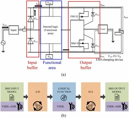
Fig.1 Diagram of the a internal structure of a digital component and b equivalent hybrid behavioral-physical model
Therefore, this study focuses on the TID effect on the input/output ports of a component.The aim of this study is to estimate the degradation of the electrical characteristics of the output port caused by the TID effect.This is achieved by applying a hybrid model that considers the TID effect of MOSFETs with ports.

Fig.2 (Color online) Process of modeling method of TID effect for digital component
Figure 2 shows the modeling method of the TID effect for digital components based on the IBIS model, which can be divided into three phases: modeling the golden effect,modeling the TID effect, and simulation and analysis.The details of each phase are as follows:
(1) Modeling of the golden.This phase is divided into three subphases.The input buffer data within the IBIS model of the digital device were preprocessed in the first subphase to produce characteristic curve data that represent theV-Icharacteristics of the diodes in the input buffer.Subsequently, the physical characteristic parameters of the diodes in the input buffer were extracted using their physical equations.The output buffer data within the IBIS model of the digital component were processed in the second subphase to generate characteristic curve data that represented theV-Icharacteristics of the transistors in the output buffer.The physical characteristic parameters of the transistors in the output buffer were extracted using their physical equations.
After the first and second subphases, the specific parameter values of the diodes and transistors in the I/O buffer can be obtained.The characteristic parameters were then described as input and output buffer models using VHDL-AMS.Based on the datasheet of the digital component, the logical function of the component is described as a functional model in the third subphase using VHDL.
By the end of the first phase, the three previously mentioned models were integrated into the golden model of the digital component, which is based on the input and output buffer models, as well as the functional model.The resulting model takes the form of an executable program file that can implement the behavioral function of the digital component while also reflecting the physical characteristics of the ports.
The delay information in the golden model was obtained by consulting the device data sheet.
(2) Modeling of the TID Effect.The second phase of the proposed TID effect modeling method is the reconstruction of the golden model generated in the first phase.In this phase, TID variables are added to the golden model based on the influence of TID effects on CMOS digital components, including threshold voltage drift, carrier mobility degradation, and timing degradation, to describe the impact of the TID on CMOS digital components and create an entire TID effect model of the digital component.
The threshold voltage and carrier mobility for the TID effect were extracted from the measuredV-Icurves, whereas the delay information for the TID effect was obtained from the measuredV-Tcurves.
(3) Simulation and Analysis.Simulation and comparative analysis of the TID model constituted the third phase.In this phase, the TID model was loaded into the simulation environment SystemVision, and the simulation results were generated.The simulation results were then compared with the experimental results, and the accuracy of the modeled results and feasibility of the proposed method were verified.
2.2 Data Pre-processing and feature extraction
2.2.1 Characteristic curve of the clamp diode at the input port
The power-clamp data within the IBIS model describe the voltage—current relationship of the input port when input voltageVinsurpasses the component supply voltage VCC.During this period, as shown in Fig.3a, the input port ground-clamp diode reverses the cutoff, whereas the power supply clamps the positive conduction of the diode.
Given that the reverse current of the diode is significantly smaller than its forward conduction current and that the input buffer inverter-gate leakage current is negligible,it can be assumed that this dataset corresponds to theVIcharacteristic curve of the power supply clamp diode.Notably, the IBIS model indicates that voltageVtablewithin the power-clamp data table adheres to the following relationship:
where VCC is the power supply voltage andVinis the voltage of the input pin.When analyzing theV-Icharacteristics of a power supply clamp diode, the corresponding voltageVshould be obtained using the following transformation:
Similarly, the GND clamp refers to the voltage of the input pins and current characteristics when the input voltage is below the GND level.During this moment, the powerclamp diode reverses, and the ground-clamp diode conducts positively (Fig.3b).Consequently, the GND clamp data represent theV-Icharacteristic curve of the ground-clamp diode.VoltageVtablein the GND clamp data table has the following relationship according to the IBIS model:
whereVGNDis the voltage of the ground; thus, to extract theV-Icharacteristics of the ground-clamp diode, voltageVmust be obtained using the following transformation:
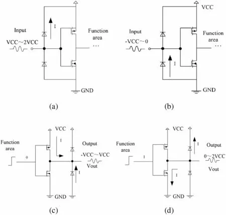
Fig.3 Schematic of the V-I characteristic curve extraction of the component for the a power clamp, b GND clamp, c pullup, and d pulldown
2.2.2 Characteristic curve of the transistor at the output port
The driver inverter and ESD protection circuit are the major components of the output port of the digital component.Different types of output buffers exist, such as push-pull,I/O, and open-drain buffers.Each buffer type has a different circuit structure and function.Consequently, theV-Icurves for the different buffer types differ; an illustration of the fundamental push—pull output is presented along with an explanation of methods to extract the transistor characteristic curve for the port circuit.Notably, this extraction approach is also applicable to other buffer types with minor modifications, as required.
The pullup curve shows the voltage—current relationship of a pin when the output state was set at one.The pullup PMOS is enabled at this time, whereas the pulldown NMOS is disabled.A scan voltage in the range of —VCC~2 VCC was applied to the output pin to obtain the voltage—current relationship.According to the IBIS model, voltageVtable,described in the pullup datasheet, is defined as
To extract the output characteristics of the pullup PMOS, theV-Idata must be obtained inside the —VCC~VCC range of the output pin voltageVout, which corresponds to the 2 VCC to 0 V interval of the pullup curve.Figure 3c shows the state of the output port during this period.
In addition, the IBIS output buffer model pulldown data can be used to determine the pulldown curves of NMOS and power-clamp diodes.The pulldown curves show the relationship between the voltage and current of the pin when the output state is set at zero.During this period, the pullup PMOS was disabled, and the pulldown NMOS was enabled.Subsequently, scan voltages ranging from —VCC~2 VCC were applied to the output pin.The voltage—current relationship was determined for the output pin.The data between 0 and 2 VCC are captured on the Pulldown curve.The voltage and current at the output pin were observed at this stage, as shown in Fig.3d.
2.3 Feature extraction
2.3.1 Extract model parameters of clamp diode In the previous section, we discussed a method for obtaining the electrical characteristics of transistors using the IBIS model.The following section focuses on the method for selecting a suitable physical model of the transistor for parameter extraction.
The model equation for a diode based on semiconductor physics [31] can be expressed as follows:
whereIsrepresents the reverse-saturation current with a typical value ranging from 10× 10-6A to 20× 10-6A;VDis the junction voltage, which equals the diode terminal voltage minus the parasitic resistance drop;VTis the thermal voltage constant with a typical value of 25.8 mV at 25°C; andnrepresents the emission coefficient.
The reverse-saturation currentIs, emission coefficientn,and parasitic resistanceRgovern the DC behavior of a diode.Modeling only the essential parameters while leaving the other parameters at their default values is acceptable.
To obtain the values of the parasitic resistanceR, emission coefficientn, and reverse-saturation currentIs, reference point coordinates were first selected from the forward characteristic curve of the diode.These coordinates were substituted into Eq.(6), to determine the parameter values.
In this study, a classic digital component CMOS noninverting multiplexer, NC7SZ157, was used as an example to demonstrate the modeling process.The golden parameter values of the diode for NC7SZ157 were obtained, as listed in Table 1, using the diode characteristic parameter-extraction technique along with a datasheet search.These values were established as a part of this study.Notably, when analyzing the IBIS model of NC7SZ157, the power-clamp diode was not included.Therefore, only the ground-clamp diodes are listed in Table 1.The input model parameters for the TID effect were extracted using the same method based on measured IBIS experimental data.
2.3.2 Extract model parameters of a MOSFET
(i) Threshold voltageVth
The threshold voltage is the turning point for the formation of the inverse layer of the MOS component,and a conduction channel is formed when the gate voltage is greater than the threshold voltage.Numerous methods for extracting the MOSFET threshold voltage exist, such as the line extraction, constant current, leakage current second-order derivative, transconductance extraction,Y-function, and beta-function methods [32, 33].In this study, the linear extrapolation method was chosen for threshold voltage extraction because of its suitability for components with different channel lengths and its potential to make full use of the transistor output characteristics.
The linear extrapolation method is based on the principle that whenVdsis small, the MOSFET output characteristics can be expressed as
whereWis the gate width,μnis the carrier mobility,Coxis the capacitance of the gate-oxide unit area, andLis the gate length.For a givenVdsdrain currentIdsdepends linearly on gate voltageVgs.The straight line with the steepest slope can be identified by extrapolating the component transfer characteristics.The intersection of this line with the horizontal axis (Vgs) indicates the threshold voltage.The reason for choosing the point with the maximum slope is that the subthreshold current dominates the curve whenVgsis small, whereas the carrier mobility decreases with increase in gate voltage whenVgsis large.
(ii) Saturation voltageVsat, saturation currentIsat,conductance parameterKn, and channel-length modulation coefficientVA
When the MOSFET operates in the linear region, the relationship between the drain voltage and the current is as follows [10]:
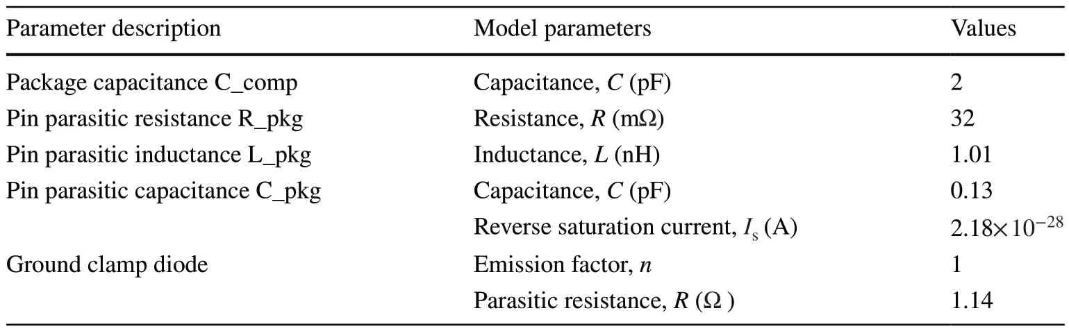
Table 1 Golden model parameters of the input port
whereAbulkis the body charge effect coefficient andEcis the critical electric field for velocity saturation.
To extract the values of the saturation voltageVsat,saturation currentIsat, conductance parameterKn, and channel-length modulation coefficientVA, the reference point coordinates are selected from the linear region of the output characteristic curve of the MOS transistor.These coordinates were substituted into Eq.(8) to obtain parameter values.
Consequently, the parameters associated with the shortchannel model of the MOSFET were successfully extracted.The extracted NC7SZ157 output buffer golden model parameters are listed in Table 2 (Vgs= 3.3 V).The output model parameters for TID effect were extracted using the same method, based on the measured IBIS experimental data.
2.4 Modeling the TID effect of a CMOS digital IC
2.4.1 Effect of ionizing radiation on the electrical properties of MOS components
The TID effect causes two types of charge traps to form within the oxide of the MOS components [34, 35]: fixed oxide charge (Not) and interface-trapped charge (Nit).These charges are responsible for changes in the electrical behavior of the components, resulting in a number of events, such as threshold voltage drift and carrier mobility degradation.
According to recent studies, the threshold voltages of NMOS and PMOS tend to decrease with increase in TID.However, NMOS exhibits a rebound effect at higher doses[36].In addition, the TID effect results in a decrease in the carrier mobility of the MOS device and, hence, a decrease in transconductance.Because of the profound effect of carrier mobility attenuation on the MOS device transconductance and current-handling capability, this effect requires careful consideration when analyzing the TID effects of MOS devices [37, 35].
Changes in the threshold voltage and carrier mobility can affect the conduction resistance of the transistor at the output of the component, increasing the conversion time.This occurs during a rising-edge transition when the NMOS transistor is gradually turned offand the PMOS transistor is gradually turned on.The conversion time of the waveform is related to the conduction resistance of the PMOS transistor and size of the load capacitor.The TID effect causes a negative drift in the threshold voltage of the PMOS and a decrease in the channel carrier mobility, that is, an increase in the on-state resistance, which leads to an increase in the time constant of the RC circuit formed by this equivalent resistance, port parasitic or load capacitance, and a longer rise time.During a falling-edge transition, the PMOS transistor gradually turns off, the NMOS transistor gradually turns on, and the parasitic or load capacitance is dischargedthrough the NMOS transistor.TID irradiation can cause both the threshold voltage and carrier mobility of the NMOS transistor to decrease, and because the effect of the two on the conduction resistance is opposite, their mutual canceling effect results in a less pronounced change in the falling-edge waveform compared to the PMOS transistor with varying TID.

Table 2 Golden model parameters of output port
2.4.2 Behavior-physical hybrid model of CMOS digital IC
In this study, a CMOS non-inverting multiplexer, NC7SZ157,was used as a case study to illustrate the process of creating a hybrid model, as shown in Figs.1b and 2.The gold functional area, input buffer, and output buffer models of NC7SZ157 were developed as the first steps of this process.
(i) Modeling of functional area
The functional domain of the behavioral-physical model of the hybrid digital IC pertains to the description of the logic function of the component being investigated along with its digital behavior.The complexity of this module varies, depending on the function and size of the device being studied.Constructing the model as a separate and callable module facilitates ease of readability and future modifications, which is highly recommended.To illustrate the efficacy of this concept, the paper employed the NC7SZ157 datasheet to describe the functional area in VHDL,as indicated in Alg.1.The input ports in Alg.1 are denoted asS,I0, andI1, respectively.In contrast,Zdenotes the output port of NC7SZ157.
Algorithm 1Behavior model of functional for NC7SZ157

?
(ii) Modeling of Input Port
Based on the model parameters in Table 1, a physical model of the input port for the NC7SZ157 was designed using VHDL-AMS, as shown in Alg.2.
Algorithm 2Physical model of input port for NC7SZ157

?
(iii) Modeling of output port
The physical model of the output port for NC7SZ157 was designed using VHDL-AMS, as shown in Alg.3, based on the model parameters listed in Table 1.
Algorithm 3Physical model of output port for NC7SZ157

?
The functional area should be combined with the input and output port models to form a golden model of the component.Figure 4a shows the simulation results of the golden model using the SystemVision software.The golden delay can be obtained from the component datasheet (the propagation delaysI0,I1andS—Zare 3.2 ns).The propagation delay is defined as the measurement starting when 50% of the rising or falling edge of the input signal arrives and ending when 50% of the rising or falling edge of the output signal is reached, as shown in Fig.4.The simulation parameters are as follows: the inputI0is set to state ‘0’,I1is set to state ‘1’,the input clock is set to 50 MHz, and the output load is set to 1 k Ω.A comparison of the datasheet and simulation results confirms that the logic function of the developed model is accurate, and that the model is capable of reproducing the analog electrical characteristics of the port.
2.4.3 Time degradation modeling
To accurately simulate the impact of the TID on digital combinatorial and sequential logic, timing degradation must be considered, which can cause changes in circuit propagation delay and even disrupt the sequential logic function.As shown in Alg.4, it is necessary to reconstruct the functional domain of the hybrid model and introduce a pin-to-pin signal propagation delay to model the propagation delay.
Algorithm 4Timing degradation model of the functional area for NC7SZ157

?
In Algorithm 4, delay_I1, delay_I0, and delay_s are introduced as three parameters representing the pin-to-pin signal propagation delay from input ports I1, I0, andSto output portZ.The preradiation delay can be obtained from the component data.TID experiment results show that the propagation delay of NC7SZ157 inS-Zpath is 3.2 ns at 0 krad(Si), 3.9 ns at 50 krad(Si), and 4.3 ns at 100 krad(Si).The simulation results are presented in Fig.4b.
From Fig.4b, it is clear that the signal transmission delay gradually increases as the TID increases.It can be concluded that the above model accurately represents the radiationinduced timing degradation of the component.Therefore, the proposed modeling method presented in this paper is feasible.

Fig.4 Simulation results for NC7SZ157 of a Golden model; b Time degradation caused by TID effect
2.4.4 Modeling TID effect of output port
The effect of the TID on the output port can be modeled by considering two key factors: the TID-induced effect on the threshold voltage and the carrier mobility of the port-transistor, as described in the Introduction section of this chapter,on the effect of the TID on digital devices.To demonstrate the feasibility of this modeling approach, a CMOS output inverter circuit was constructed, as shown in Fig.5a, in the SystemVision simulation environment.
In Fig.5a, the load capacitanceC1 and resistanceR1 were as 2 pF and 1 k Ω , respectively.The simulation results shown in Figs.5b show that the electrical characteristics of the pullup PMOS can be changed by adjusting the threshold voltage and carrier mobility.The conduction cases one—four reflect an increase in the threshold voltageof the PMOS and a decrease in the carrier mobility of the PMOS.It can be observed that, with an increase in the threshold voltage and a decrease in the carrier mobility of the pullup PMOS, the PMOS on-resistance increases,leading to an increase in the rise time of the level at the output pinVoutand a decrease in the high-level amplitude.Therefore, the inclusion of the TID effect of the output pin threshold voltage of the transistor and carrier mobility in the model allows for the representation of the TID-related variation in the CMOS device port characteristics.

Fig.5 Schematic of a inverter circuit for CMOS and b Simulation result of (a)
Figure 5b are intended to verify the TID effect modeling method, in which the threshold voltage (Vth) and conductance parameters (Kn) are added to the port.During the modeling of the TID effect, the threshold voltage (Vth)and conductance parameter (Kn) of the device at different dose points were extracted by measuring the transfer characteristic curve of the transistor at the port of the TID experiment.Subsequently, the extractedVthandKnare used as generic parameters for Alg.3 to obtain simulation results for the TID effect at the port, as shown in Fig.7.
3 Experiments and results
3.1 Experimental setup
To verify the TID effect modeling method for the CMOS digital IC proposed in this study, an experimental circuit for a CMOS non-inverting multiplexer, NC7SZ157, was set up.Subsequently, the TID experiment was conducted at the Xinjiang Technical Institute of Physics and Chemistry, Chinese Academy of Sciences.The experimental board and the TID experimental environment are shown in Fig.6.The experimental conditions are presented in Table 3.

Fig.6 (Color online) TID Experiment platform
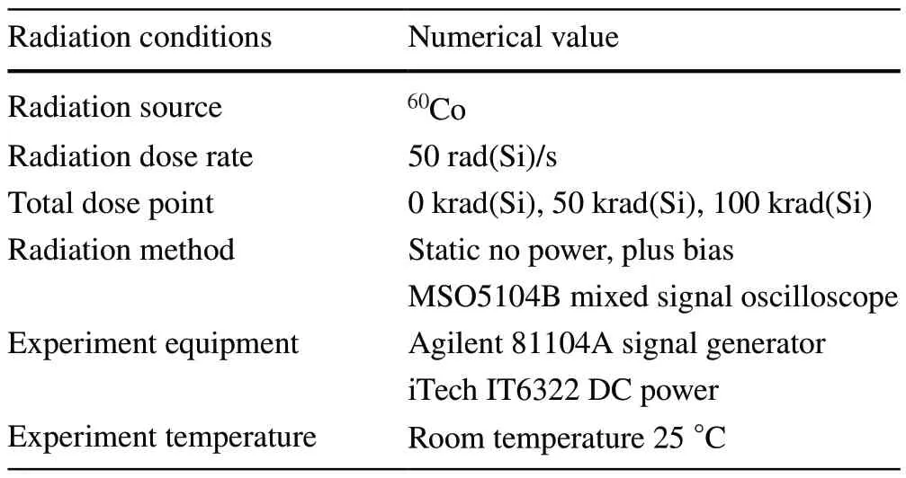
Table 3 TID Experiment Conditions
3.2 Results and discussion
When measuring the experimental data, theI0pin of NC7SZ157 was set to ‘0’, theI1pin was set to ‘1’, and a 40 kHz square wave signal was applied to theSpin to measure the IBIS model andV-Twaveform data of the output portZat different dose points.The IBIS model primarily includes theV-Icurves of the port diode and transistor,which are used to extract the characteristic parameters of the diode and transistor, and are substituted into Algs.2 and 3 as generic parameters for the simulations.TheV-Tcurve was compared with the simulation results, as shown in Fig.7.It can be observed that the rise timetrand fall timetfof the simulation and experimental results increase with an increase in the TID.trandtfrefer to the times required for the output voltage of a component to change from 10% to 90% and from 90% to 10%, respectively.
The edge times of the experimental results are compared with those of the simulation results in Table 4.It can be seen thattrandtfincrease with an increase in the TID.The relative error between the experimental and simulation results was calculated using theV-Tdata shown in Fig.7.The relative error is defined as the average ratio of the difference between the experimental and simulation results to the experimental results for the voltage values within one period.The obtained relative errors were 0.2%,0.6%, and 1.4% for dose points 0 krad(Si), 50 krad(Si),and 100 krad(Si), respectively.The results show that the model accurately reflects the effect of the TID on the CMOS digital IC termination.Table 4 also shows that the experimental results at 50 krad(Si) are close to the simulation results at 0 krad(Si) and that the experimental results at 100 krad(Si) are close to the simulation results at 50 krad(Si).This was because of the limited accuracy of the SystemVision simulation environment.In future studies, we aim to enhance the accuracy of the model and simulation to achieve a closer match between the simulation and experimental results.In addition, all the simulations were completed in less than 1 s, indicating the high efficiency of the model.
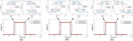
Fig.7 Comparison of experiment results with simulation results at a 0 krad(Si); b 50 krad(Si) and c 100 krad(Si)
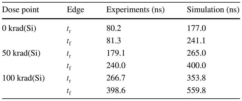
Table 4 Comparison of simulation and experiment results
4 Conclusion
This study proposes a three-phase TID effect modeling method for CMOS ICs based on the IBIS model to address the problems raised by transistor-level modeling when evaluating the TID effect in digital ICs.In the first phase,a gold model of a digital IC was developed.The transistor characteristic curves of the input and output buffers were first processed using the IBIS model of the component, and the physical parameters of the input and output ports were extracted using the diode and MOS physical equations.The VHDL language was used to model the functional areas of the components according to the truth table in the datasheet.The golden digital IC model was developed by combining the port and functional area models.In the second phase, the gold model is reconstructed based on the TID effect on the CMOS threshold voltage drift, carrier mobility degradation, and timing degradation effects to form the final TID effect model of the digital IC.In the third phase, the TID effect experiments were conducted using a CMOS non-inverting multiplexer, NC7SZ157,as an example.The 40 kHz waveform information of the NC7SZ157 output was measured at 0 krad(Si), 50 krad(Si), and 100 krad(Si), and the IBIS model was obtained to extract the feature parameters.The TID effect model was then loaded into the SystemVision environment for simulation.Finally, the simulation and experimental results were compared, which indicated that the relative error between the simulation and experimental results at each dose point was less than 2%.Thus, the feasibility and accuracy of the proposed modeling method were confirmed.The TID effect of other CMOS digital ICs can be simulated using this modeling method to evaluate their ability to tolerate the TID effect.
Author ContributionsAll authors contributed to the study conception and design.Material preparation, data collection, and analysis were performed by JHL, XPZ, GL, WDT, and XDZ.The first draft of the manuscript was written by BL and all authors commented on previous versions of the manuscript.All authors read and approved the final manuscript.
Data availabilityThe data that support the findings of this study are openly available in Science Data Bank at https://cstr.cn/31253.11.sciencedb.14189 and https://www.doi.org/10.57760/sciencedb.14189.
Declarations
Conflict of interestThe authors declare that they have no competing interests.
 Nuclear Science and Techniques2024年2期
- Nuclear Science and Techniques的其它文章
- Measurement of the neutron-induced total cross sections of natPb from 0.3 eV to 20 MeV on the Back-n at CSNS
- Nuclear charge radius predictions by kernel ridge regression with odd-even effects
- Unbound 28 O, the heaviest oxygen isotope observed: a cutting-edge probe for testing nuclear models
- Development of CONTHAC-3D and hydrogen distribution analysis of HPR1000
- A fast forward computational method for nuclear measurement using volumetric detection constraints
- Artificial neural network-based method for discriminating Compton scattering events in high-purity germanium γ-ray spectrometer