An ISGW Filtering Antenna with Spurious Modes and Surface Wave Suppression for Millimeter Wave Communications
Lihui Wang ,Dongya Shen ,Qiuhua Lin ,Zhiyong Luo ,Wenjian Wang,3 ,Jianpei Chen ,Zhao Gao,Wei Zhang
1 School of Electronics and Communication Engineering,Sun Yat-sen University,Shenzhen 518107,China
2 School of Information Science and Engineering,Yunnan University,Kunming 650091,China
3 Kuang-Chi Institute of Advanced Technology&State Key Laboratory of Meta-RF Electromagnetic Modulation Technology,Shenzhen,China
4 School of Electrics and Information Engineering,Yunnan Minzu University,Kunming,China
5 Institute of Telecommunication and Navigation Satellites,China Academy of Space Technology,Beijing 100094
*The corresponding author,email: shendy@ynu.edu.cn
Abstract: In this paper,an integrated substrate gap waveguide (ISGW) filtering antenna is proposed at millimeter wave band,whose surface wave and spurious modes are simultaneously suppressed.A secondorder filtering response is obtained through a coupling feeding scheme using one uniform impedance resonator (UIR) and two stepped-impedance resonators(SIRs).To increase the stopband width of the antenna,the spurious modes are suppressed by selecting the appropriate sizes of the ISGW unit cell.Furthermore,the ISGW is implemented to improve the radiation performance of the antenna by alleviating the propagation of surface wave.And an equivalent circuit is investigated to reveal the working principle of ISGW.To demonstrate this methodology,an ISGW filtering antenna operating at a center frequency of 25 GHz is designed,fabricated,and measured.The results show that the antenna achieves a stopband width of 1.6f0(center frequency),an out-of-band suppression level of 21 dB,and a peak realized gain of 8.5 dBi.
Keywords: filtering antenna;integrated substrate gap waveguide;millimeter wave communications;spurious modes suppression;surface wave suppression
I.INTRODUCTION
The development of millimeter wave communication systems has led to a trend in designing low-loss,highly integrated,and multifunctional components[1–3].As a multi-functional integrated component,the filtering antennas have become a research hot spot in recent years due to promising performance.[4].
According to previous studies,filtering antennas can be divided into two categories [5].One approach [6]to achieve a filtering response is by using the radiator as the last-stage resonator of the filtering circuit.In this study,microstrip terminated coupled lines and a rectangle patch were utilized as first-and secondorder resonators,respectively.As a result,a secondorder filtering response was achieved with a center frequency of 25 GHz and a relative bandwidth of 3%.Another method [7] for obtaining a filtering property is proposed through the design of a radiator or feeding structure with a filtering function.The antenna achieved radiation nulls by utilizing E-plane parasitic patches,a metasurface unit with multi-folded Ushaped slots,and a defected ground structure.However,it is important to note that the filtering antennas aforementioned have a narrow stopband width.
As shown in Figure 1,interference between adjacent frequency bands due to spurious modes is a pressing issue for filtering antennas.A study [8] demonstrated that a filtering antenna with a suppression level of 23 dB and a stopband width of 2.3f0was achieved by selecting a proper length ratio of two sides of the patch.However,it is difficult to integrate into planar circuits due to its high profile.In order to improve integration,several wide-stopband filtering antennas were proposed based on a substrate integrated waveguide(SIW)technology[9,10].In[9],a SIW filtering antenna with loading metal-insulator-metal capacitors was presented to excite multiple resonance modes.The antenna offered a stopband suppression of 1.46 times the center frequency of the second passband (f2),but the gain is only 4.85 dBi.In a recent study [10],a SIW millimeter wave filtering antenna with an out-of-band suppression of 20.55 dB was proposed benefiting from the cutoff characteristics of SIW.Combination of SIW and complementary split-ring resonator,a stopband width of 1.57f0was obtained.Nevertheless,SIW technology is associated with high radiation loss,particularly at millimeter wave band.
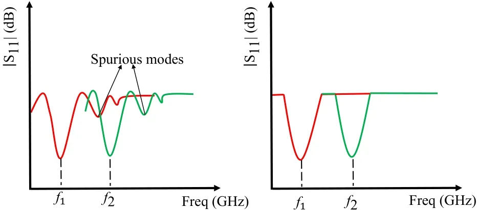
Figure 1. Spurious modes interference.
ISGW is a PCB process waveguide technology with the advantages of low weight,low radiation loss,and easy integration at microwave and millimeter wave band.Thanks to the excellent waveguide characteristics of ISGW,several antennas with promising performance have been proposed[11–14].For instance,[13]employed the ISGW technology to suppress the leakage and surface wave of the horn antenna,achieving a gain of 11.5 dBi and a bandwidth of 20.5% in Ka-Band.In [15],a millimeter wave ISGW leaky-wave antenna with a gain of 17.6 dBi was proposed.Due to the advantage of low loss and less dispersive propagation characteristics at millimeter wave band.Consequently,the radiation efficiency of the antenna is over 86%.Although these antennas exhibit excellent performance at the millimeter wave band,the interference of spurious is a challenge.Moreover,surface wave radiation is also an urgent issue,especially at the millimeter wave band.
To address the aforementioned issues,a novel feeding scheme with filtering function is proposed in this paper,which suppresses spurious modes and surface wave radiation simultaneously.By reasonably utilizing the frequency cutoff characteristics of ISGW,a filtering antenna with an out-of-band suppression of 21 dB and a suppression width of 1.6f0is achieved.Furthermore,the impedance matching level of the antenna is improved by 5 dB benefiting from the ISGW’s ability to bind the electric field.Compared to the previous filtering antennas,the advantages of the proposed one are as follows.
1.A novel feeding scheme is presented,which increases the filtering function without occupying additional circuit area and design complexity.
2.The surface wave and spurious modes are simultaneously suppressed by ISGW,which effectively solves the problem of spurious modes interference in conventional filtering antennas.
Section II shows the configuration and working principle of the proposed antenna.The mechanism of spurious modes and surface suppression is studied in Section III.The measured results and a brief discussion are given in Section IV.Finally,a conclusion is drawn in Section V.
II.DESIGN AND WORKING PRINCIPLE OF THE ANTENNA
2.1 Filtering Antenna Configuration
The proposed filtering antenna configuration consists of four stacked layers,as illustrated in Figure 2.The upper surface of layer#1 is printed with periodic rectangular radiation patches,which serve as both the radiation structure and the last-order resonator of a second-order filtering response.The integrated substrate gap waveguide(ISGW)is composed of layer#2,layer #3,and layer #4.A metal layer etched I-type coupling aperture is printed on the lower surface of layer#1.The lower surface of layer#2 contains a feeding line comprising of two stepped-impedance resonators (SIRs) and one uniform impedance resonator(UIR).To provide more flexibility in the alignment of the feeding line,an isolation layer (layer #3) is sandwiched between layer#2 and layer#4.Layer#4 contains metal vias that are embedded in its interior and are connected to circular metal arrays on its upper surface and a metal layer on its lower surface.The four layers are supported by Rogers 4003C (The relative permittivity and loss tangent are 3.38 and 0.0027,respectively).Vertical coupling is utilized for filtering response without occupying additional space.Moreover,the impedance matching can be improved by adjusting the width of the slot between radiation patches.The optimized parameters of the proposed filtering antenna are listed in Table 1.
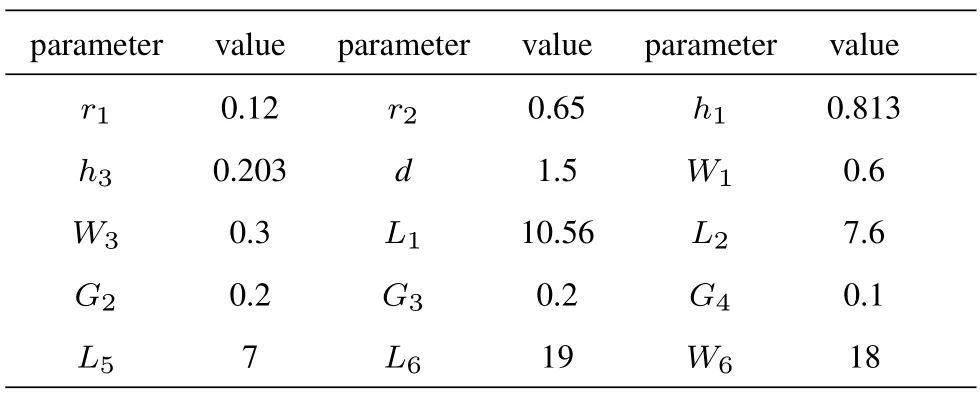
Table 1. Parameters of the proposed antenna(unit:mm).
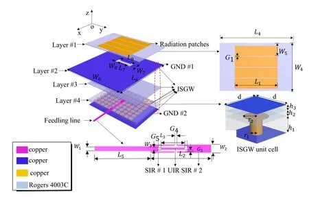
Figure 2. Configuration of the proposed filtering antenna.
2.2 The Filtering Principe
The proposed filtering antenna with a center frequency(f0) of 25 GHz,0.3-dB ripple level,and a fractional bandwidth(FBW)of 9%utilizes filter synthesis technology [16] for its design.The lumped circuit model of the proposed filtering antenna is shown in Figure 3.The first-order resonator is represented by a parallel circuit of inductorL1and capacitanceC1,which includes UIR and SIR #1.Similarly,the second-order resonator is represented by the parallel circuit of inductorL2,capacitanceC2,and radiation resistanceRload,which is formed by the coupling between SIR#2 and radiation patches.The coupling between the first-order resonator and the second-order resonator is denoted by an admittance inverterJ12.For the lowpass filter(LPF)prototype,the elements values are as follows:g0=1.000,g1=1.1805,g2=0.6957,andZ0=Rload=50 Ω.The lumped element values are calculated using equations(1)through(4)[17],resulting inC2=0.98 pF,L1=L2=41.18 pH,Qe=13.1,andM12=0.0993.
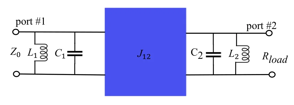
Figure 3.The lumped circuit model of the proposed filtering antenna.
whereQeandM12are the external quality factor and coupling coefficient,respectively.
The reflection coefficient(S11)and transmission coefficient (S21) [18] of the two-port network shown in Figure 3 are expressed as equations(5)and(6),respectively.
whereA,B,C,andDare the transmission matrix of this filtering circuit as shown in Figure 3.
The coupling coefficient (M12) and external quality factor(Qe)are extracted[16]using ANSYS HFSS with equations (7) and (8).Figure 4 shows that the values ofM12andQeare determined byG4andG5.Specifically,whenG4is 0.1 mm andG5is 0.3 mm,M12andQeare equal to 0.0993 and 13.1,respectively.
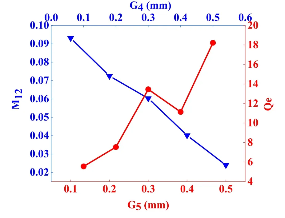
Figure 4. Coupling coefficient M12 and external quality factor Qe.
wheref0is the center frequency and Δf±90°is the frequency difference between-90°and +90°of the reflection coefficient;f1andf2are the resonant frequencies of the first-order resonator and the secondorder resonator,respectively.
After utilizing aforesaid theory to guide the design of the filtering response of the antenna,the resonator and radiation patches are combined for tuning.According to [6,19],as the antenna is a single-port device and the gain is comparable to the filter’s insertion loss,the nulls of antenna radiation at certain frequencies correspond to the transmission zeros of the filter.The simulated normalized gain curve of the proposed filtering antenna is then compared to the normalized|S21|curve of the synthesis,calculated using equation(6).
As observed in Figure 5,the simulated operating frequency band of the proposed filtering antenna is from 23.8 GHz to 26.1 GHz(|S11|<-10 dB).Good selectivity is achieved by two degenerate modes resonating at 24.2 GHz and 25.7 GHz,which supports the proposed antenna to obtain good selectivity.The two radiation nulls are generated at 19.3 GHz and 29.6 GHz,the gain curve of the filtering antenna exhibits a steeper sideband roll-off and the out-of-band suppression level is 21 dB.Furthermore,the high unloaded quality of the ISGW contributes to the frequency selectivity.The simulated normalized gain curve of the filtering antenna and the curve of transmission coefficient obtained by the synthesis technology show good agreement.
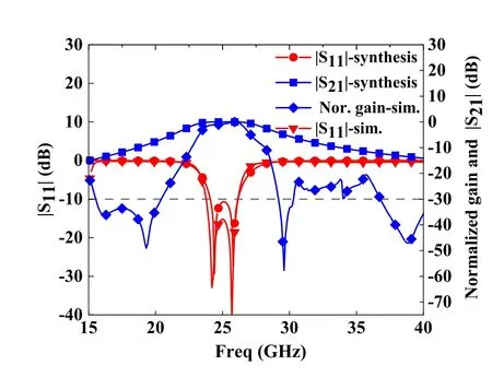
Figure 5. Comparison of S-parameter and normalized gain response.
2.3 Resonance Analysis
In order to effectively excite the resonance of the proposed antenna,a circuit model based on transmission line analysis of the aperture-coupled microstrip antenna[20]shown in Figure 6 is proposed.This model considers four rectangular microstrip patches as equivalent to four transmission lines,each with a characteristic impedance ofZpand length ofL1.The model is taken into account the propagation of TEM waves along the x-axis direction.
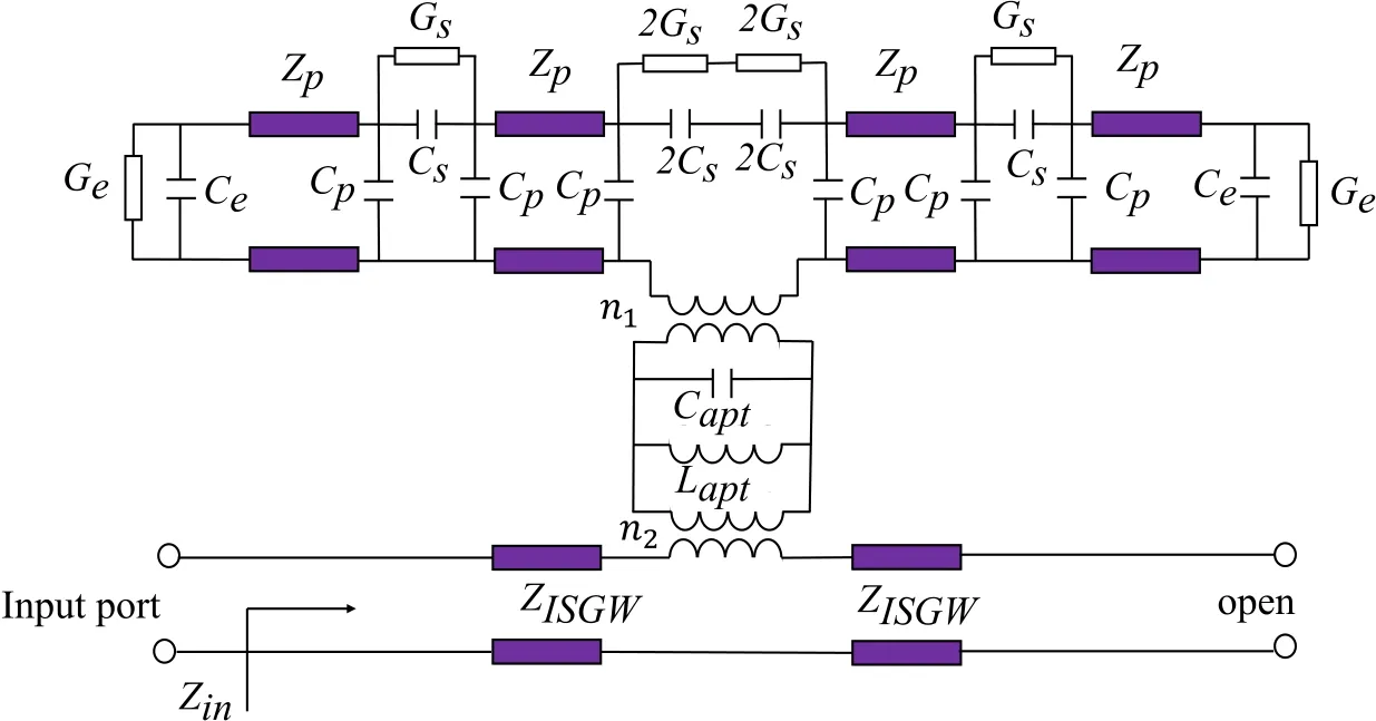
Figure 6. Equivalent circuit model of the proposed antenna.
CsandCprefer to the series capacitance and parallel capacitance of the gap between radiation patches,respectively.The variablesCeandGerepresent the fringe capacitance and radiation conductance of the radiation patches,respectively.The energy transfer coefficientsn2andn1indicate the transfer of energy from the ISGW feeding line to the coupling aperture and from the coupling aperture to the radiation patches,respectively.The coupling aperture is represented by the capacitance ofCaptand the inductanceLapt.The characteristic impedance,phase shift constant,and physical length of the ISGW terminal opening line are represented byZISGW,βISGW,andLISGW,respectively.The values ofn1,n2,andLaptcan be approximated as follows:
where the parametersZapt,ϵre,andL7refer to the characteristic impedance,effective dielectric constant,and length of the coupling aperture,respectively.The symbolscandfrepresent the speed of light in vacuum and operating frequency,respectively.
To determine the capacitance of the radiation gap,the Y-parameters are extracted using the equivalent circuit in Figure 7.According to Figure 8,when the width of the radiation gap between the radiation patches of the filtering antennaG1is 0.12 mm,CsandCpare calculated as 0.23 pF and 0.09 pF,respectively.
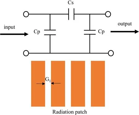
Figure 7.Equivalent circuit model of the radiation patches.
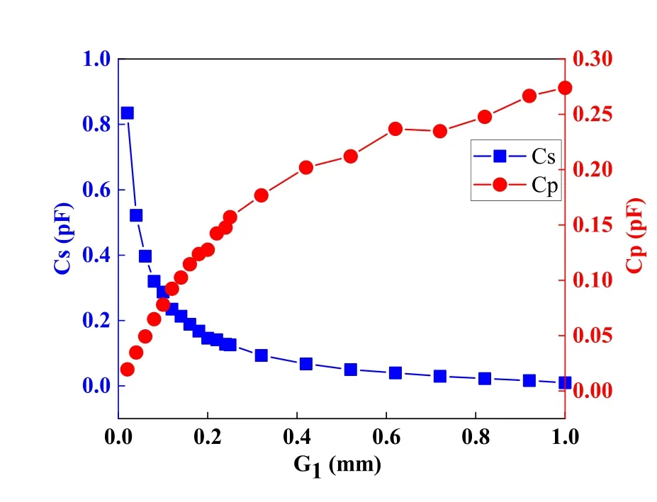
Figure 8. Cp and Cs.
The values ofn1andn2can be calculated using equations (9) and (10),and are found to be 0.99 and 0.24,respectively.The equivalent capacitance of the coupling aperture can be determined using the equivalent circuit illustrated in Figure 7.Specifically,when the aperture width is 0.5 mm,the capacitance(Capt)is calculated to be 0.45 pF.Additionally,the equivalent inductanceLaptof the coupled aperture can be determined using equation (11) and has been reported in various studies[20–23]to be 1.1 nH.Finally,according to[24],we can calculateGe=0.0073 S,Gs=0.0073 S,andCe=0.159 pF.
To assess the accuracy of the equivalent circuit model,a comparison of the input impedance between the calculated results obtained from the equivalent circuit model using Advanced Design System(ADS)and the synthesis technology is conducted.The comparison is presented in Figure 9,where the blue line represents the results obtained from the equivalent circuit model using Advanced Design System,and the red line depicts the theoretical value of the synthesis technology.The results in Figure 9 show that the resonant frequency obtained from the equivalent circuit model closely matches the resonant frequency obtained from the synthesis technology.The equivalent circuit model proves to be a useful tool in establishing the relationship between the resonant frequency and the physical parameters of the proposed antenna.
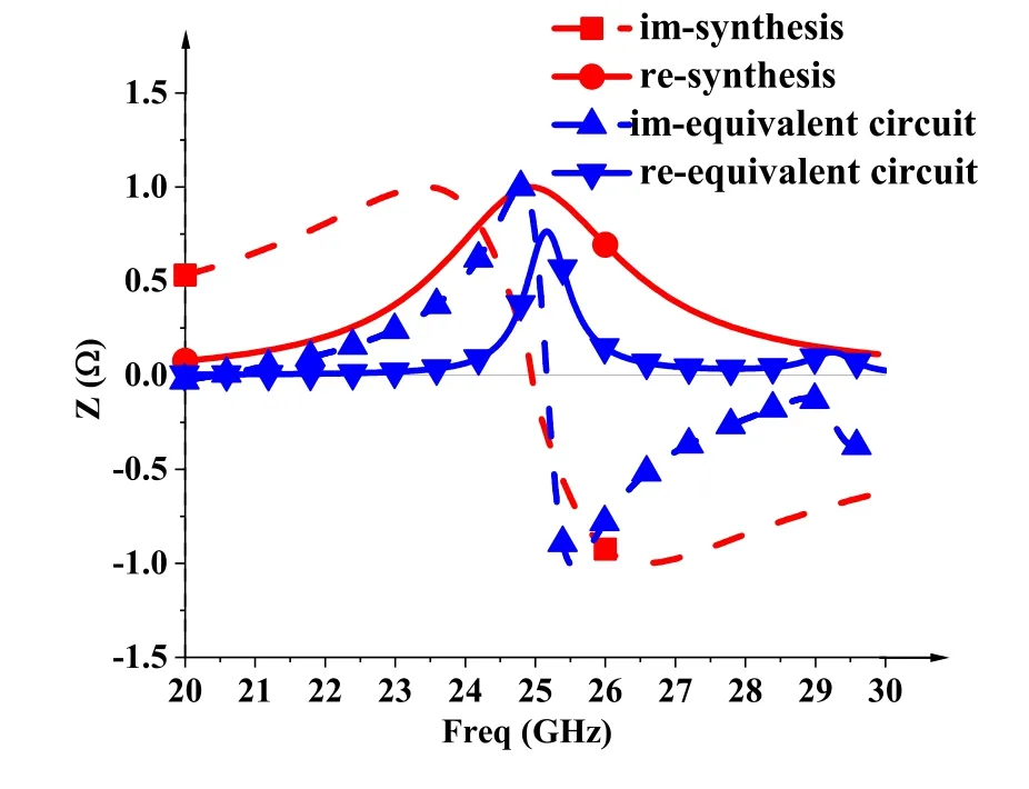
Figure 9. Input impedance curve.Note: re: real parts of the impedance.im: imaginary parts of the impedance.
III.MECHANISMS OF SPURIOUS MODES AND SURFACE WAVE SUPPRESSION
In order to reveal the suppression of spurious modes and surface wave radiation in ISGW [25],an equivalent circuit model of the ISGW unit cell is investigated.The period length of the unit cell is denoted byd,whilegrepresents the width between the unit cells.The circular metal patch and via diameters are represented byd2andd1,respectively.As shown in Figure 10,the ISGW unit cell can be equivalent to a transmission line with a characteristic impedance ofZISGWand a phase constant ofβ[26],where the electromagnetic wave propagates in the X-direction.The inductance of the via is represented byL,while the capacitance between GND #1 and GND #2 is denoted asCm.Furthermore,C3refers to the capacitance between the circular metal patch and GDN#2.These parameters can be calculated using equations(12),(13),and(14)from[27].To design the ISGW,equations(5)and (6) provide insight into the reflection coefficient and transmission coefficient of Figure 10(b).
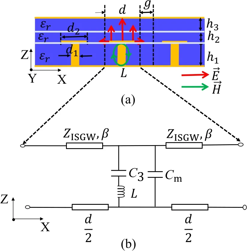
Figure 10. ISGW unit cell.(a)Configuration.(b)Equivalent circuit model.
The dispersion diagram of ISGW is analyzed using ANSYS HFSS,as shown in Figure 11.The results indicate that the low-frequency cutoff frequency(fL)of ISGW decreases from 18.3 to 15.6 GHz as the diameter(d1)of the metal via decreases from 0.6 to 0.4 mm.From Figure 11(a),it is observed that whend1is less than 0.4 mm,the slope offHis greater thanfL,and on the contrary,whend1is greater than 0.4 mm,the slope offHis less thanfL,and thus it can be concluded that the bandwidth obtains its maximum value atd1=0.4 mm.Similarly,it is observed from Figure 11(b) that whend2is less than 1.3 mm,the slope offLis less than that offH.On the contrary,whend2is greater than 1.3 mm,the slope offLis greater thanfH.This implies that the maximum bandwidth is achieved atd1=0.4 mm ord2=1.3 mm.Consequently,it can be concluded that the electromagnetic stopband width of ISGW can be effectively expanded by selecting the appropriate sizes of its unit cell.
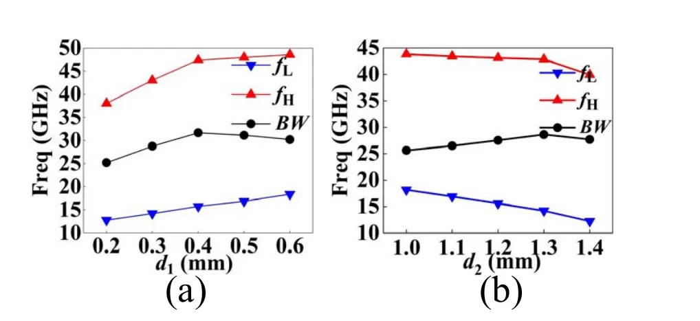
Figure 11.ISGW cut-off frequencies under different parameters.(a)d1.(b)d2.
In order to demonstrate the effectiveness of ISGW in suppressing spurious modes,ANSYS HFSS is utilized to calculate the frequencies of these modes while varying ISGW unit cell sizes.The spurious modes frequencies are plotted in Figure 12.As seen in Figure 12(a),a decrease in via diameter from 0.6 to 0.2 mm resulting in a decrease in the frequency of the spurious mode in the low-frequency sideband(f1)of the filtering antenna,from 20.4 to 14.5 GHz.However,the center frequency (f0) of the proposed filtering antenna and the frequency of the spurious mode in the high-frequency sideband(f2)remains.This phenomenon confirms the idea of Figure 11(a).Based on the observations from Figure 12(b),it shows that the frequency of spurious mode in the low-frequency sideband of the filtering antenna decreases from 18.0 GHz to 13.8 GHz as the diameter of the circular metal patch of ISGW increases from 1.1 to 1.4 mm.However,the frequency of spurious modes in the high-frequency sideband remains unaffected.This aligns with the conclusion drawn from Figure 11(b),which suggests that the spurious mode is suppressed due to the electromagnetic stopband characteristic of ISGW.It is worth noting that the proposed filtering antenna’s passband performance remains unaltered when appropriately adjustingd1andd2.
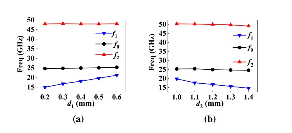
Figure 12. Spurious modes frequencies under different parameters.(a)d1.(b)d2.
The simulated|S11|and transverse electric field distributions of the proposed antenna (with ISGW) and the reference antenna (without ISGW) are shown in Figure 13 and Figure 16,respectively.The proposed antenna successfully suppresses spurious modes at 20.25 GHz compared to the reference antenna,as seen in Figure 13.Specifically,the frequency of spurious modes in the lower sideband shifts from 22.05 GHz to 15.3 GHz,and in the upper sideband it shifts from 33.3 GHz to 46.8 GHz with ISGW loading.Furthermore,the simulation results in Figure 13 demonstrate a 5 dB improvement in impedance matching level with the loading of ISGW,which is supported by the simulation results presented in Figure 14.
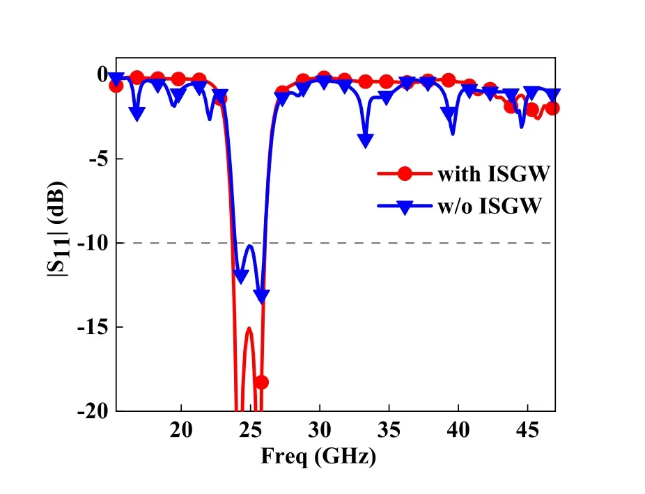
Figure 13. Suppression of spurious modes by ISGW.Note:w/o: without.
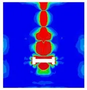
Figure 14. Electric field distributions on GND.(a)15 GHz,(b)50GHz,(c)24 GHz,(d)26GHz.
The confinement of electromagnetic (EM) energy around the feeding line is demonstrated in Figure 14(c)and (d),while a significant leakage of EM energy is observed outside the ISGW stopband (shown in (a)and (b)).This indicates that the ISGW helps improve impedance matching by confining the EM energy within the desired frequencies.
Figure 15 illustrates the suppression effect of ISGW on surface waves.The comparison between Figure 15(a) and (b) shows that the proposed antenna’s surface wave radiation is effectively suppressed by ISGW while enhancing its broadside radiation capability.This phenomenon is attributed to the bounding ability of ISGW on the edge electric field,as shown in Figure 16.Loading ISGW reduces the scattering level of the fringe electric field by 19 dB.
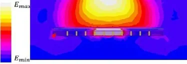
Figure 15. The effect of ISGW on surface wave radiation.(a)Without ISGW.(b)With ISGW.
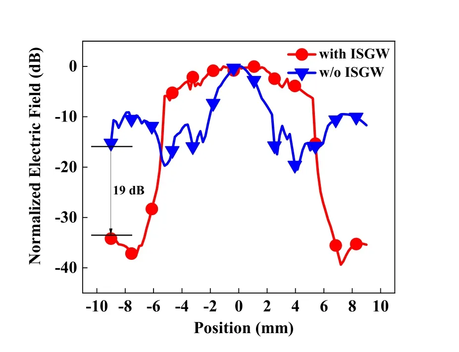
Figure 16. Effect of ISGW on transverse electric field distributions.
To improve impedance matching and suppress spurious modes,parametric studies are carried out.Observed from Figure 17,a proper number of ISGW unit cells not only suppress spurious modes but also improve impedance matching level and remain the resonant frequency (mandndenote the number of unit cells of ISGW in x-axis and y-axis,respectively).Furthermore,the resonant frequency and matching level can be tuned by changing the length of the radiation patchL1(See Figure 18(a)) and the width of gapG1(See Figure 18(b)),respectively,which can be explained by the circuit model in Figure 6.
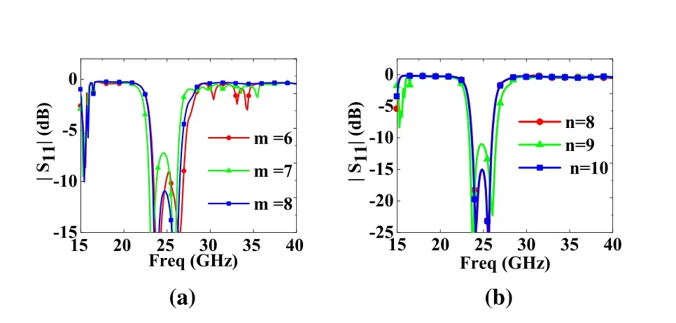
Figure 17. |S11|under different parameters.(a)m.(b)n.Note:m and n denote the number of unit cells of ISGW in x-axis and y-axis,respectively.
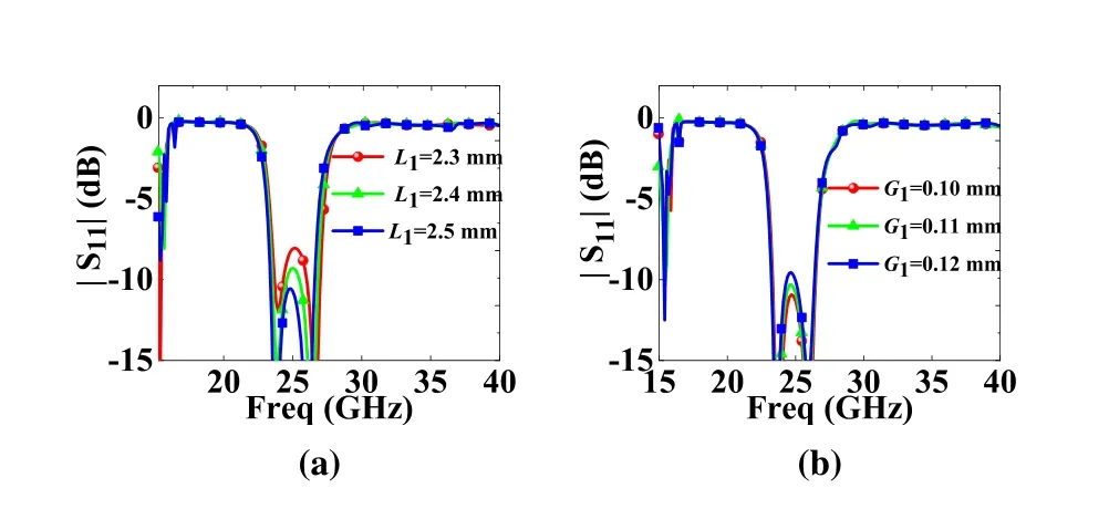
Figure 18. |S11| under different parameters.(a) L1.(b)G1.
IV.MEASUREMENT AND DISCUSSION
As depicted in Figure 19,the S-parameter of the proposed antenna is measured by an Agilent vector network analyzer,and the gain and radiation patterns are measured in the anechoic chamber system.Observed from Figure 20,the simulated and measured|S11|demonstrates the same operating bandwidth covering from 23.6 GHz to 25.7 GHz.

Figure 19. Measurement setup.(a)S-parameter measurement setup.(b)Radiation pattern measurement setup.
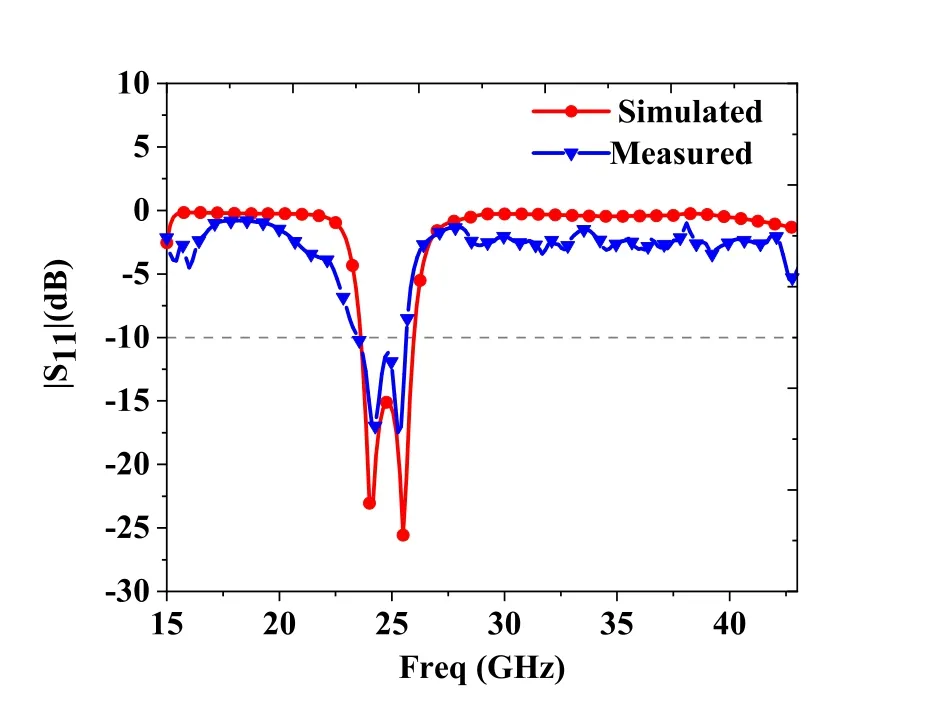
Figure 20. Measured and simulated reflection coefficient.
Figure 21 plots the measured and simulated realized gain at different frequencies.It can be observed that the proposed antenna’s peak realized gain is 8.5 dBi both in the simulation and measurement.Figure 22 presents the measured and simulated radiation patterns of the proposed filtering antenna at 24 GHz,25 GHz,and 26 GHz.The figure illustrates that the antenna exhibits stable radiation performance across the three different frequencies,which can be attributed to the suppression of surface wave radiation by ISGW.And due to the symmetry of the proposed filtering structure,the cross polarization of this antenna is low.The discrepancies between simulated and measured results are mainly attributed to discontinuities at the SMA joint welds and air gap introduced between adjacent layers of dielectric plates[31].In addition,the alignment mismatch of the far-field measurement system introduces errors in the measured and simulated gains[32].
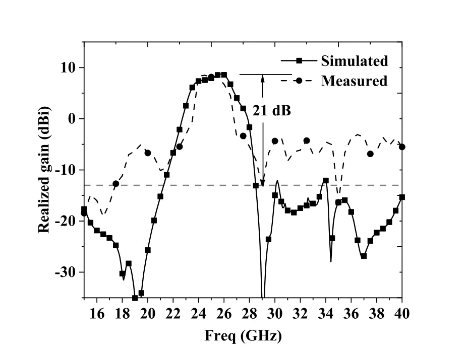
Figure 21. Measured and simulated realized gain.

Figure 22. Measured and simulated patterns at different frequencies.(a) 24 GHz.(b) 25 GHz.(c) 26 GHz.Note: sim.:simulation.mea.: measurement.E/H:E/H-plane.co-plo: co-polarization.cross-plo: cross-polarization.
Table 2 displays a performance comparison between previous studies and the proposed filtering antenna.The table includes six indicators: technology(Tech.),center frequency(f0),gain,suppression level(Supp.),suppression width,and whether surface wave radiation can be suppressed (Surface wave supp.).When compared to other studies such as[9],[10],and[28],the proposed filtering antenna exhibits a wider stopband and higher average realized gain than the four antennas listed in the table.Although the gain of the proposed filtering antenna may be lower than that of[10],it is important to note that at the millimeter wave band,the radiation loss of substrate integrated waveguide(SIW)is greater than that of integrated substrate gap waveguide(ISGW).The gain and rejection levels of the antenna presented in[28]are higher than those of the proposed antenna,but its suppression width is limited to only 1.02 times the center frequency.In contrast,the proposed antenna not only suppresses surface waves but also spurious modes,making it a more versatile option.Additionally,its integration with planar circuits based on ISGW technology is easier.Therefore,the proposed antenna shows promise as a potential candidate for millimeter wave communications.
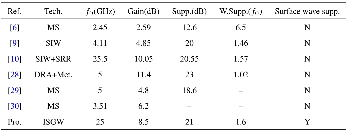
Table 2. Comparison with previous studies.
V.CONCLUSION
This paper presents an ISGW filtering antenna for millimeter wave applications.The ISGW technology is developed to suppress spurious modes and surface wave simultaneously and its transmission mechanism is studied using an equivalent circuit model.By selecting the appropriate size for the ISGW unit cell,the stopband width of the antenna is increased by 20.05 GHz,and the fringe electric field that causes surface wave is effectively suppressed by 19 dB.The proposed filtering antenna,which has a suppression of 21 dB and a peak realized gain of 8.5 dBi,is designed,fabricated,and measured.The proposed filtering antenna is a good candidate for 5G millimeter wave communication systems due to the suppression capability of interference and surface wave.
ACKNOWLEDGEMENT
This work was supported by the National Key research and development program of China (No.2021YFB 2900401),the national natural science foundation of China (No.62361057,No.61861046),the key natural science foundation of Shenzhen(No.JCYJ20220818102209020),and the key research and development program of Shenzhen (No.ZDSYS20210623091807023).
- China Communications的其它文章
- Secure and Trusted Interoperability Scheme of Heterogeneous Blockchains Platform in IoT Networks
- Intelligent Edge Network Routing Architecture with Blockchain for the IoT
- Privacy-Preserving Deep Learning on Big Data in Cloud
- PowerDetector: Malicious PowerShell Script Family Classification Based on Multi-Modal Semantic Fusion and Deep Learning
- Dynamic Task Offloading for Digital Twin-Empowered Mobile Edge Computing via Deep Reinforcement Learning
- Resource Trading and Miner Competition in Wireless Blockchain Networks with Edge Computing

