First⁃Principles Calculations on Electronic Structures and Optical Properties of g⁃C3N4Nanoribbons
DU Xiu‑JuanMA Ke‑RongZHANG Zheng‑WeiYANG WenZHANG RuiZHANG Qing‑Mei
(1School of Applied Science,Taiyuan University of Science and Technology,Taiyuan 030024,China)
(2Department of Chemistry and Chemical Engineering,Jinzhong University,Jinzhong,Shanxi 030619,China)
(3Shanxi Key Laboratory of Metal Forming Theory and Technology,School of Material Science and Engineering,Taiyuan University of Science and Technology,Taiyuan 030024,China)
Abstract:The first‑principles method based on density functional theory was performed to investigate the electronic structure and optical properties of the armchair nanoribbons(AC‑g‑C3N4NRs)and zigzag g‑C3N4nanoribbons(ZZ‑g‑C3N4NRs).The results show that the edge H atoms of AC‑g‑C3N4NRs and ZZ‑g‑C3N4NRs can exist stably.The valence band maximums(VBMs)of AC‑g‑C3N4NRs are mainly contributed by most of N atoms,whereas the VBMs of ZZ‑g‑C3N4NRs are contributed by the N atoms near the CH edge.The conduction band minimums(CBMs)of AC‑g‑C3N4NRs mainly belong to C and N atoms near the one edge or two edges of AC‑g‑C3N4NRs,while the CBMs of ZZ‑g‑C3N4NRs mainly belong to C and N atoms near the NH edge of ZZ‑g‑C3N4NRs.The absorption coefficient and the reflectivity of AC‑g‑C3N4NR or ZZ‑g‑C3N4NR increased with the increasing width of the corresponding nanoribbon.An obvious blueshift phenomenon of the absorption coefficient could be generated in the low‑energy range as the width of AC‑g‑C3N4NR increased.
Keywords:g‑C3N4nanoribbons;binding energies;electronic structure;optical properties;first‑principles calculations
0 Introduction
As a low‑cost,high‑stable,nontoxic and visible‑light‑responsive photocatalyst,graphitic carbon nitride(g‑C3N4)has a multifunctional application in photocata‑lytic hydrogen evolution[1‑3],CO2reduction[4‑5]and photo‑catalytic degradation of pollutants[6‑7].In order to fur‑ther enhance the photocatalytic performance of g‑C3N4,bulk g‑C3N4is usually cut into nano‑sized g‑C3N4,such as g‑C3N4nanosheets[3,8‑11]and g‑C3N4nanoribbons(g‑C3N4NRs)[12‑13],which possesses favorable photocatalyt‑ic activity because of the larger specific surface area with abundant active sites and short diffusion distance of photogenerated charge carriers.
Due to the quantum size effect,the properties of g‑C3N4NRs are considerably different from those of g‑C3N4nanosheets.In experiments,Wang et al.have successfully synthesized the Mn‑doped g‑C3N4NR cata‑lyst by a two‑step calcination method[13].Zhao et al.have fabricated g‑C3N4NR on graphene sheets by using a simple one‑step hydrothermal method[12].However,lit‑tle attention is paid to theoretical research on the arm‑chair nanoribbons(AC‑g‑C3N4NRs)or zigzag g‑C3N4nanoribbons(ZZ‑g‑C3N4NRs)which can be obtained by cutting nanosheets along specific directions,and thus the electronic and optical properties of these above two g‑C3N4NRs as function of widths are not clear.Expo‑sure of these properties will help the design and fabri‑cation of g‑C3N4NRs‑based electronic and optical devices in experiment.
In this work,the rest of the paper is organized as follows:the computational method and models of AC‑g‑C3N4NRs and ZZ‑g‑C3N4NRs with the width of 7(i.e.the number of the atom chains)are given in Section 2.The binding energies,band gaps,band structure,par‑tial charge density,partial density of states and optical properties of g‑C3N4NRs are analyzed and the conclu‑sions are drawn in the last section.
1 Computational method and models
The computation of electronic and optical proper‑ties was performed within the framework of the density functional theory(DFT)implemented in the Vienna ab‑initio Simulation Package(VASP)[14‑18].The electron‑ionic core interactions were treated by the projected augmented wave(PAW)potentials[19].The Perdew‑Burke‑Ernzerhof(PBE)exchange‑correlation function‑al[20]within the generalized‑gradient approximation(GGA)was used in order to yield the correct ground‑state structure of the systems.An efficient Broyden/Pulay mixing scheme[21‑22]was used for the mixing of the charge density.The cut‑off energy of the plane waves was 500 eV.The energies and the forces on each ion were converged to less than 10-5eV·atom-1and 0.1 eV·nm-1,respectively.The Gaussian smearing broad‑ening was chosen as 0.05 eV.The Brillouin zones were sampled by 1×1×11 and 1×1×25 K‑point meshes according to Monkhorst‑Pack scheme[23]for calcula‑tions of electronic structures and optical properties,respectively.The number of energy bands was in‑creased to 300 when the optical properties were com‑puted.The absorption coefficient and reflectivity can be derived from the computational dielectric func‑tion.Compared with the experiment value 2.7 eV,the computed band gap of bulk g‑C3N4was 1.28 eV and the difference in band gap was 1.42 eV.The same conclu‑sion is also drawn by Wu et al[24].However,the PBE computations can still reveal the variation tendency of the electronic structures and optical properties.
The width of AC‑g‑C3N4NR(or ZZ‑g‑C3N4NRs)was classified by the number of the atom chains NA(or NZ)across the ribbon width and denoted as NA‑AC‑g‑C3N4NR(or NZ‑ZZ‑g‑C3N4NR).In the present work,we focus our attention on the structures of AC‑g‑C3N4NR and ZZ‑g‑C3N4NRs with the width NAor NZ=4~10.As examples,geometry structures of 7‑AC‑g‑C3N4NR and 7‑ZZ‑g‑C3N4NR are shown in Fig.1a and 1b,respective‑ly.g‑C3N4NRs periodically extend along the z direction.To avoid the interactions between the neighboring rib‑bons,g‑C3N4NRs were separated from each other by the vacuum region with 1.6 nm in both edge‑to‑edge(i.e.x direction)and layer‑to‑layer(i.e.y direction).
2 Results and discussion
2.1 Binding energies and band gaps
The binding energies Ebare usually adopted to investigate the binding strength between H atoms andg‑C3N4NRs.Ebwas computed according to Eb=(Epassivated-Ebare-nEH)/n,where n is the number of H atoms,Epassivatedand Ebarerefer to the total energy of g‑C3N4NR with H termination and g‑C3N4NR without H termination,re‑spectively.EHis the half of the total energy of a H2mol‑ecule at 0 K and 0 GPa and was computed by equation EH=1/2EH2.The evolution of the binding energies of AC‑and ZZ‑g‑C3N4NRs as a function of the width NAor NZis shown in Fig.2a.It can be seen that the binding ener‑gies of these fourteen g‑C3N4NRs are all negative val‑ues,indicating that the edge H atoms can exist stably.The black curve and red curve represent that the bind‑ing energy of the AC‑g‑C3N4NR has a small fluctuation,whereas that of ZZ‑g‑C3N4NR has a large fluctuation with the increasing number of atom chains.In addition,the smaller binding energies of ZZ‑g‑C3N4NRs with the width NZ=4,6,8,10 indicate that H atoms are pre‑ferred to adsorb on the edges of these systems.Fig.2b displays the evolution of the band gaps of AC‑and ZZ‑g‑C3N4NRs as a function of the width NAor NZ.It can be seen from Fig.2b that the band gaps of the remaining eleven semiconductor g‑C3N4NRs present a small fluc‑tuation except for ZZ‑g‑C3N4NR with NZ=5,7,9 which are metallic systems with no band gaps.Table 1 shows the molar ratio(ε)of C and N atoms of the AC‑and ZZ‑g‑C3N4NRs.Table 1 and Fig.2 indicate that the binding energies and band gaps of AC‑g‑C3N4NRs have no obvi‑ous change rule,while ZZ‑g‑C3N4NRs have the smaller binding energies and the larger band gaps when the ε of C and N atoms is 3/4.
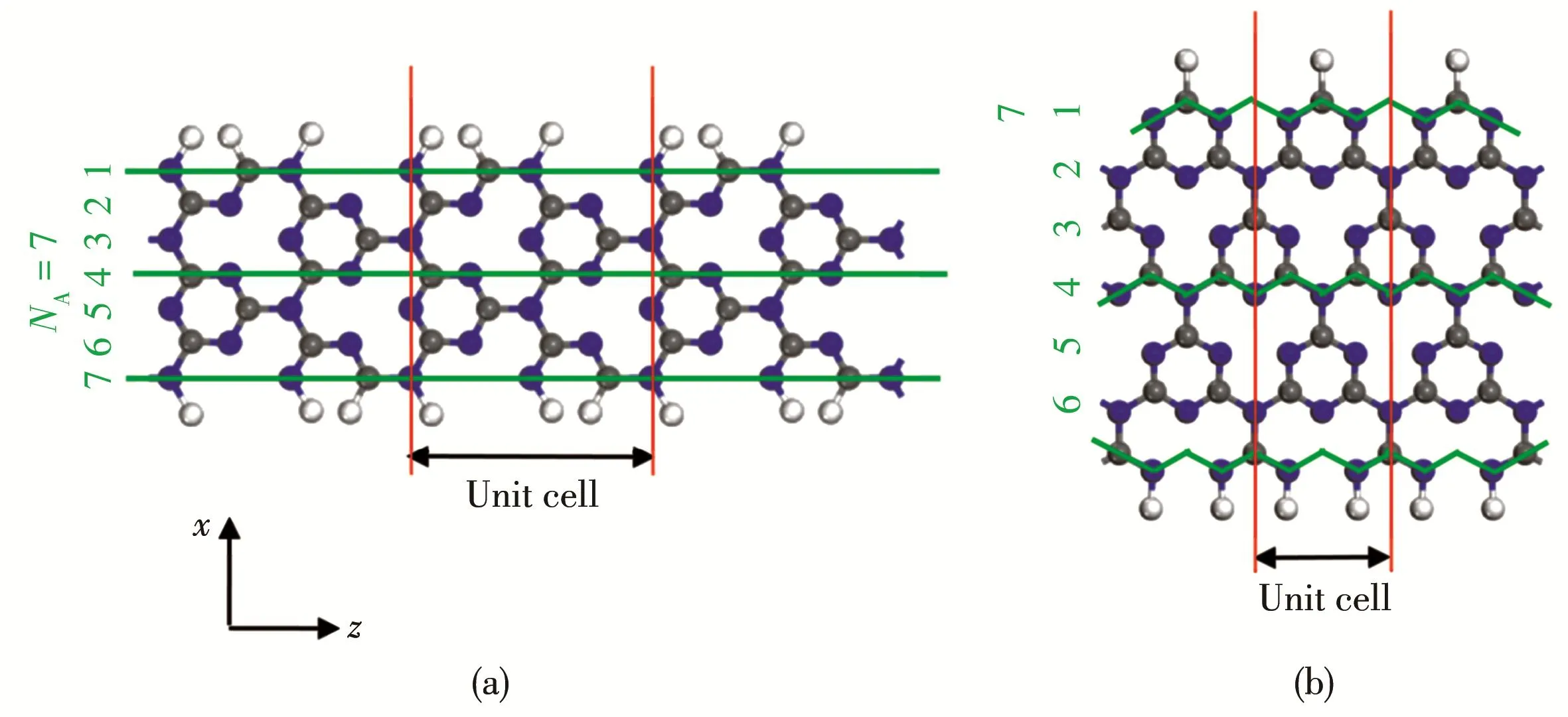
Fig.1 Geometry structures of monolayer g‑C3N4NRs with H termination:(a)7‑AC‑g‑C3N4NR;(b)7‑ZZ‑g‑C3N4NR
In the following sections,the aforementioned stable semiconductor AC‑g‑C3N4NRs with the width NA=4,7,10 and semiconductor ZZ‑g‑C3N4NRs with the width NZ=4,10 will be taken as examples for further investigating the electronic and optical properties of g‑C3N4NRs.

Fig.2 Evolution of the binding energies(a)and band gaps(b)of AC‑g‑C3N4NRs and ZZ‑g‑C3N4NRs as a function of the width NAor NZ
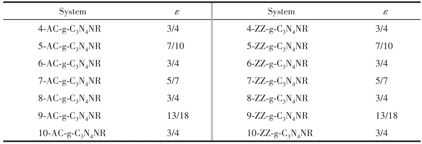
Table 1 ε of C and N atoms of AC⁃g⁃C3N4NRs and ZZ⁃g⁃C3N4NRs
2.2 Band structure,partial charge density and partial density of states
Fig.3 shows band structures of AC‑g‑C3N4NRs with(a)NA=4,(b)NA=7,(c)NA=10 and ZZ‑g‑C3N4NRs with(d)NZ=4,(e)NZ=10.Fig.3a and 3d reflect that AC‑g‑C3N4NR and ZZ‑g‑C3N4NR withNAorNZ=4 are both indirect band gap semiconductors because of the valence band maximum(VBM)and the conduction band minimum(CBM)locating at different points ofK‑space,whereas Fig.3b,3c and 3e are all the direct band gap systems due to the VBM and CBM located atΓpoint ofK‑space.
In order to intuitively recognize compositions of the VBMs and CBMs,Fig.4 shows partial charge densi‑ties for VBMs and CBMs of AC‑g‑C3N4NRs with(a)NA=4,(b)NA=7,(c)NA=10 and ZZ‑g‑C3N4NRs with(d)NZ=4,(e)NZ=10.It can be seen that the VBMs of AC‑g‑C3N4NRs(the red isosurface in Fig.4a~4c are mainly distributed on most of N atoms,whereas the VBMs of ZZ‑g‑C3N4NRs(the red isosurface in Fig.4d and 4e arecontributed by the N atoms near the CH edge.More‑over,these charge distributions contributing to VBMs are all within the g‑C3N4plane.However,the CBMs of AC‑g‑C3N4NRs(the green isosurface in Fig.4a~4c)mainly belong to C and N atoms near the one edge or two edges of AC‑g‑C3N4NRs,while CBMs of ZZ‑g‑C3N4NRs(the green isosurface in Fig.4d and 4e)mainly belong to C and N atoms near the NH edge of ZZ‑g‑C3N4NRs.Interestingly,these charge distribu‑tions are perpendicular to the g‑C3N4plane.
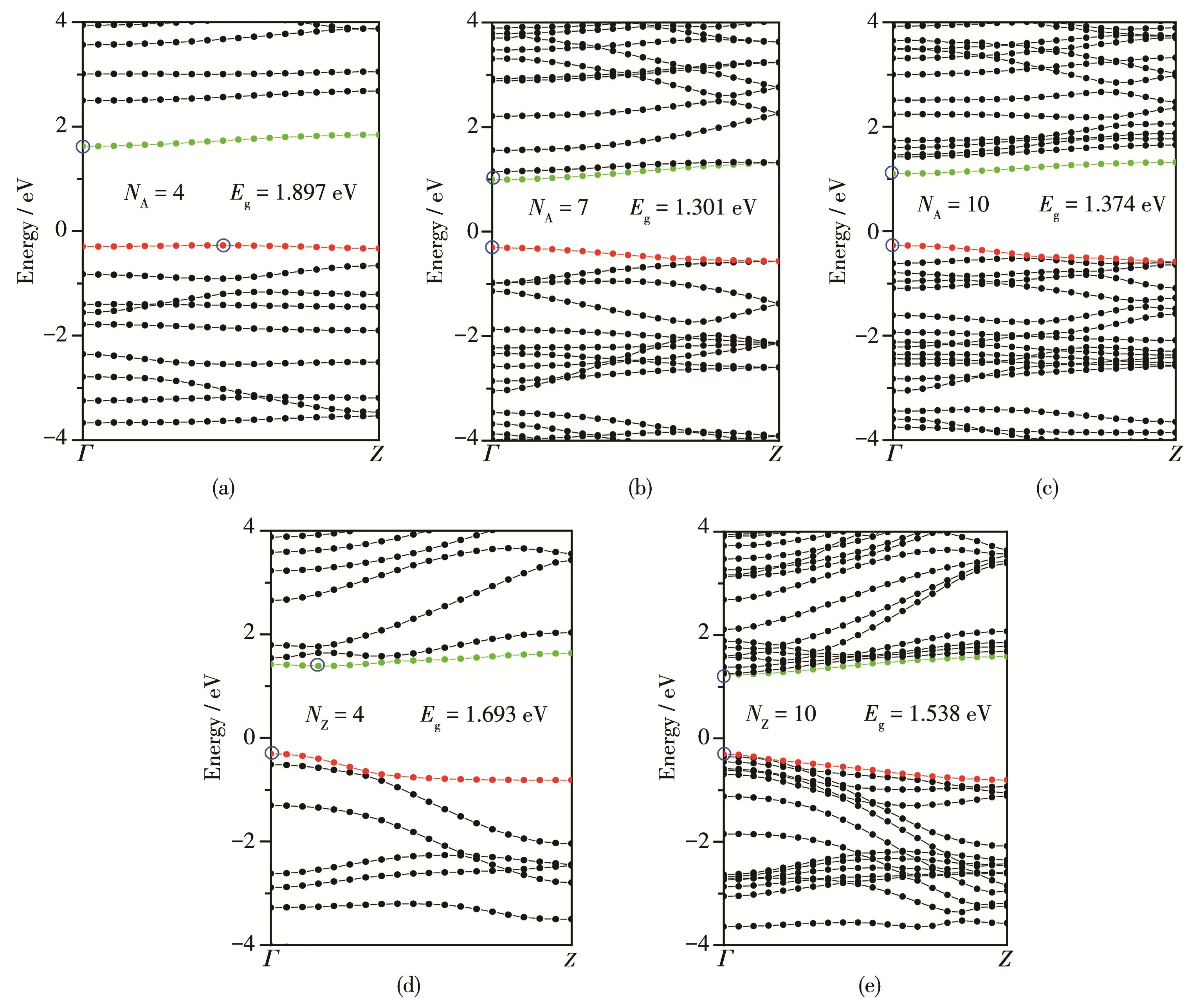
Fig.3 Band structures of AC‑g‑C3N4NRs with(a)NA=4,(b)NA=7,(c)NA=10 and ZZ‑g‑C3N4NRs with(d)NZ=4,(e)NZ=10
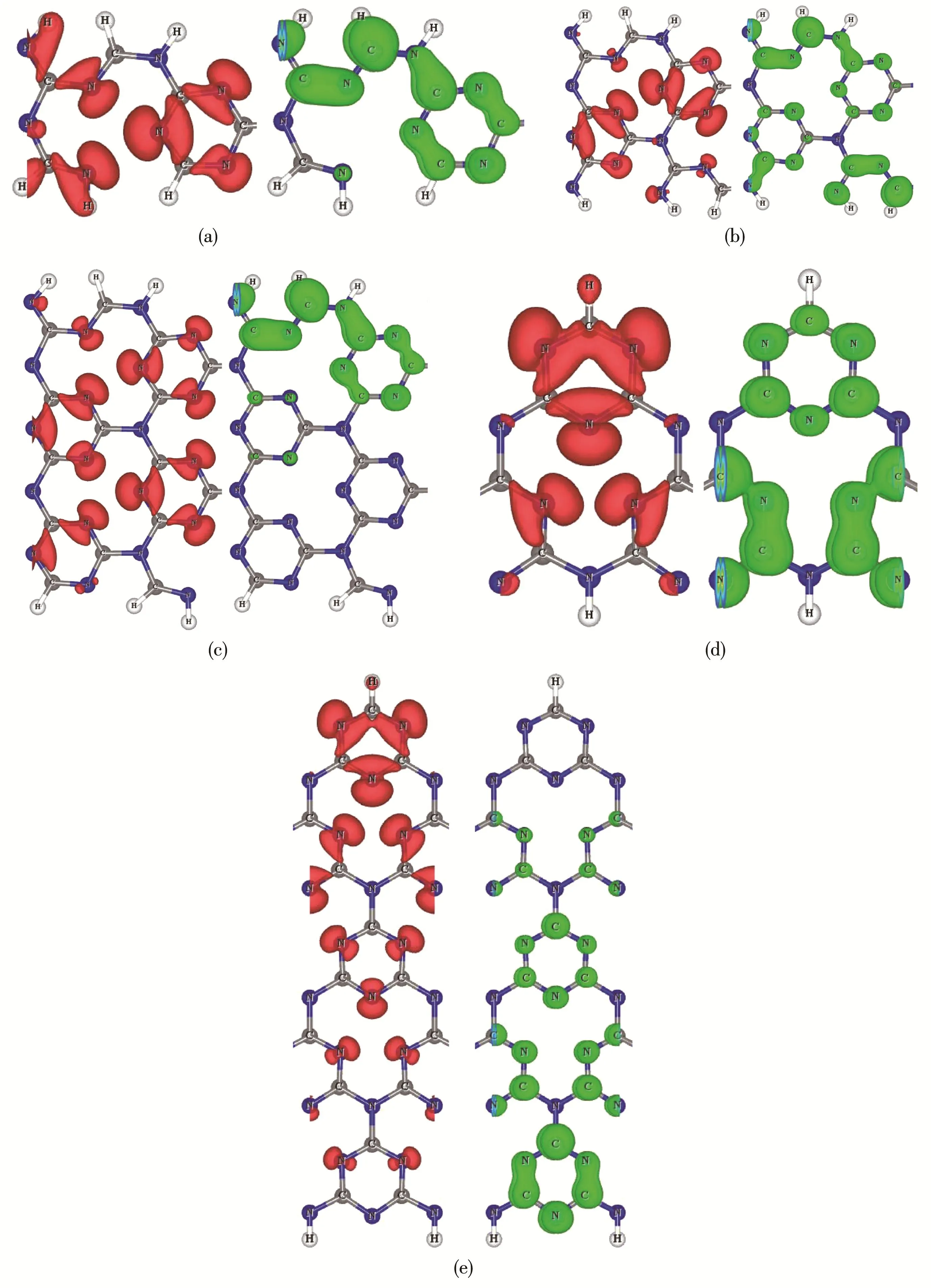
Fig.4 Partial charge densities for VBMs(red isosurface)and CBMs(green isosurface)of AC‑g‑C3N4NRs with(a)NA=4,(b)NA=7,(c)NA=10 and ZZ‑g‑C3N4NRs with(d)NZ=4,(e)NZ=10
Furthermore,we computed the partial density of states of AC‑g‑C3N4NRs with(a)NA=4,(b)NA=7,(c)NA=10 and ZZ‑g‑C3N4NRs with(d)NZ=4,(e)NZ=10.As shown in Fig.5,the VBMs of AC‑and ZZ‑g‑C3N4NRs are composed of the 2p states of N atoms,while the CBMs are mainly contributed by the 2p states of C andN atoms of the systems.In terms of element composi‑tions,this is in good agreement with the above analysis of the partial charge densities.
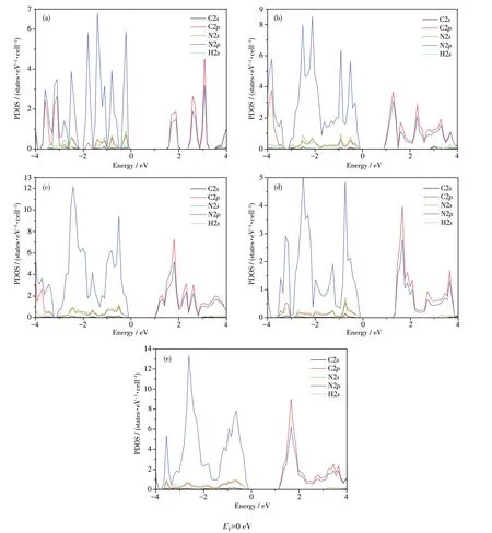
Fig.5 Partial density of states of AC‑g‑C3N4NRs with(a)NA=4,(b)NA=7,(c)NA=10 and ZZ‑g‑C3N4NRs with(d)NZ=4,(e)NZ=10
2.3 Optical properties
In the present work,for comparison,the optical properties of g‑C3N4NRs,bulk g‑C3N4and the armchair graphene nanoribbons(AC‑GNRs)are characterized by absorption coefficient(α),reflectivity(R)and energy loss(L),which are defined as follows[25‑26]:


Where the real part ε1and imaginary part ε2of the complex dielectric function ε=ε1+jε2can be obtained based on the computational electronic states,and ω is the circular frequency.
Fig.6 shows the computed optical absorption coef‑ficients of(a)AC‑g‑C3N4NRs with NA=4,7,10,(b)ZZ‑g‑C3N4NRs with NZ=4,10,(c)AC‑GNRs with NA=4,7,10 and(d)bulk g‑C3N4as a function of energy.In the work,ZZ‑GNRs are not investigated because the com‑puted band gaps are 0.Seen from the Fig.6a and 6b,the absorption coefficient of AC‑g‑C3N4NR or ZZ‑g‑C3N4NR increased with the increasing width of the cor‑responding nanoribbon.In Fig.6a,these absorption peaks of 4‑AC‑g‑C3N4NR,7‑AC‑g‑C3N4NR and 10‑AC‑g‑C3N4NR(i.e.the black,red and green absorption peaks)in the low‑energy range of 0~5 eV are specifical‑ly located at 3.58,3.84,and 4.31 eV,respectively.Therefore,an obvious blueshift phenomenon can be generated in the low ‑energy range as the width in‑crease of AC‑g‑C3N4NR.In Fig.6b,the black and green absorption peaks are respectively located at 4.28 and 4.32 eV in the low energy region,indicating that there is only a very weak blueshift.By contrast,Fig.6c dis‑plays an obvious redshift phenomenon in the low‑energy range as the width increase of AC‑GNR.Compared with bulk g‑C3N4(shown in Fig.6d),the AC‑and ZZ‑g‑C3N4NRs have the smaller absorption coefficient.
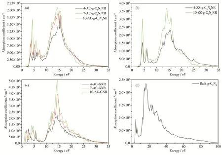
Fig.6 Computed absorption coefficients of(a)AC‑g‑C3N4NRs with NA=4,7,10,(b)ZZ‑g‑C3N4NRs with NZ=4,10,(c)AC‑GNRs with NA=4,7,10 and(d)bulk g‑C3N4
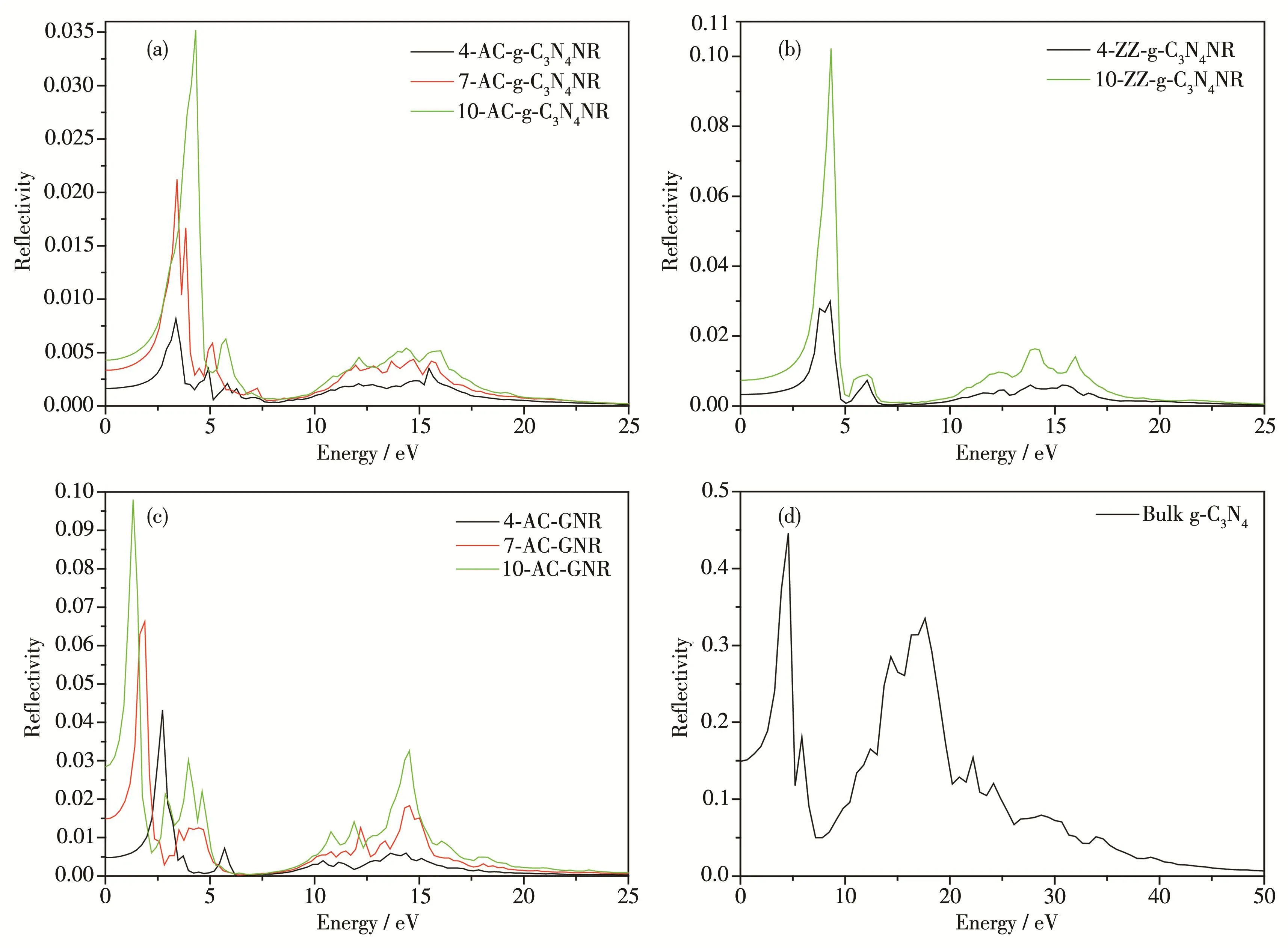
Fig.7 Computed reflectivity of(a)AC‑g‑C3N4NRs with NA=4,7,10,(b)ZZ‑g‑C3N4NRs with NZ=4,10,(c)AC‑GNRs with NA=4,7,10 and(d)bulk g‑C3N4
Fig.7 shows the computational reflectivity of(a)AC‑g‑C3N4NRs with NA=4,7,10 and(b)ZZ‑g‑C3N4NRs with NZ=4,10,(c)AC‑GNRs with NA=4,7,10 and(d)bulk g‑C3N4as a function of energy.It also can be seen from Fig.7a and 7b that the reflectivity is increasing with the increased width increase of AC‑or ZZ‑g‑C3N4NR,and the strongest reflectivities of these NRs are all in the low energy range of 2~5 eV.By contrast,AC‑GNRs can draw the same conclusion(Fig.7c).In addition,bulk g‑C3N4has a larger reflectivity compared with g‑C3N4NRs.
3 Conclusions
The electronic and optical properties of g‑C3N4na‑noribbons have been investigated by using the first‑principles calculations.The results are as follows:
(1)The edge H atoms of AC‑and ZZ‑g‑C3N4NRs studied in the present work can exist stably.AC‑g‑C3N4NRs with NA=4~10 and ZZ‑g‑C3N4NRs with NZ=4,6,8,10 are semiconductors,whereas ZZ‑g‑C3N4NR with NZ=5,7,9 are metallic systems with no band gaps.
(2)The VBMs of AC‑g‑C3N4NRs are mainly dis‑tributed on most of N atoms,whereas the VBMs of ZZ‑g‑C3N4NRs are contributed by the N atoms near the CH edge.The CBMs of AC‑g‑C3N4NRs mainly belong to C and N atoms near the one edge or two edges of AC‑g‑C3N4NRs,while the CBMs of ZZ‑g‑C3N4NRs mainly belong to C and N atoms near the NH edge of ZZ‑g‑C3N4NRs.The VBMs of AC‑and ZZ‑g‑C3N4NRs are composed of the 2p states of N atoms,while the CBMs are mainly contributed by the 2p states of C and N atoms of the systems.
(3)The absorption coefficient and the reflectivity of AC‑g‑C3N4NR or ZZ‑g‑C3N4NR are increased with the width increase of the corresponding nanoribbon.For the absorption coefficient,an obvious blueshift phe‑nomenon can be generated in the low‑energy range as the width increase of AC‑g‑C3N4NR.
Acknowledgements:The authors would like to acknowl‑edge the support from the National Natural Science Foundation of China(Grants No.11705124,51871158,11704274).
- 无机化学学报的其它文章
- Coexistence of Two Unique Cu(Ⅱ) Ions in Mononuclear Cu(Ⅱ)Complexes with Furanyl Substituted Triaryltriazoles
- Effect of Zn on Photocatalytic Activity of Block⁃Shaped Monoclinic WO3
- Synthesis,Structure,Luminescence,Photocatalytic and Magnetic Properties of a Neodymium Complex Constructed from Biphenyl⁃3,4′,5⁃tricarboxylic Acid
- Preparation and Nonlinear Absorption Properties of SiO2@CdTe@Au Composite Nanoparticles
- 二茂铁基-双酮锌配合物的合成、电化学活性及多光子吸收
- 基于(E)⁃N,N⁃二甲基⁃4⁃(2⁃(吡啶⁃4⁃基)乙烯基)苯胺的锌/镉有机-无机杂化金属卤化物的结构和发光性质

