Fabrication and opto-electronic performance of transparent conducting ZTGO thin films
2021-04-16 01:17ZHONGZhiyouTIANYuZHUYa
中南民族大学学报(自然科学版) 2021年2期
ZHONG Zhiyou, TIAN Yu,ZHU Ya
(1 College of Electronic Information Engineering, South-Central University for Nationalities, Wuhan 430074, China 2 Hubei Key Laboratory of Intelligent Wireless Communications, South-Central University for Nationalities, Wuhan 430074, China)
Abstract The ZTGO transparent conductive oxide thin films were prepared by magnetron sputtering technique.The influences of growth temperature(Tem)on the optical, electrical and opto-electronic performance of the thin films were investigated by ultraviolet-visible spectrometer, four-point probe and optical characterization methods.The results show that the Tem significantly affects the electro-optical characteristics of thin films.When the Tem is at 640 K, the prepared thin film has the best opto-electronic performance, with the electrical conductivity of 7.86×10² S·cm-1, the optical band-gap of 3.48 eV, the minimum Urbach energy of 0.167 eV, the highest average visible transmittance of 84.61% and the maximum figure of merit of 0.423 S.
Keywords magnetron sputtering; transparent conductive oxide; thin film
For the transparent electrode application in light-emitting diodes(LEDs)[1-5], photovoltaic cells(PVCs)[6-10]and liquid crystal displays(LCDs)[11-13], the transparent conductive oxide(TCO)thin films based on indium-tin oxide(ITO)have been investigated.Recently, the research on zinc oxide(ZnO)-based TCO thin films has been attracted due to nontoxicity, low cost and high stability in hydrogen plasma[14-18].ZnO is typically grown as an n-type semiconductor with energy band-gap of 3.37 eV and its electrical and optical properties are changed by doping conditions with impurities such as boron(B), aluminum(Al), gallium(Ga), titanium(Ti), zirconium(Zr), yttrium(Y)and magnesium(Mg)[19-29].It is reported that the Ti dopant can increase the electrical conductivity of ZnO-based TCO thin films, and the Ga dopant can improve the crystalline quality and increase carrier concentration of ZnO-based TCO thin films[30-33].However, the optical properties and chemical durability of the singly-doped TCO thin films is not very satisfied.In order to further improve the optical and electrical properties of ZnO-based TCO thin films, the co-doping with two elements is considered as one of effective methods.In this paper, Ti and Ga co-doped ZnO(ZTGO)thin films were fabricated on glass substrates by magnetron sputtering at various growth temperatures(Tem).The effect ofTemon optical and electrical performance of the samples was studied in terms of the meansurement of optical transmittance, electrical conductivity and figure of merit.
1 Experimental
1.1 Sample preparation
The ZTGO thin films were fabricated on glass substrates by magnetron sputtering using a radio frequency of 13.6 MHz(MS-560C).The ceramic target of ZTGO contains 1.5 wt% TiO2, 1.5 wt% Ga2O3and 97 wt% ZnO.The distance between the target and the substrate was 75 mm.The base pressure in deposition chamber was kept blow 5×10⁻⁴Pa and high purity argon(5N in purity)was used as the working gas.The glass substrates were ultrasonically cleaned in acetone, alcohol and deionized water each for 15 min before loading into the chamber.Before deposition, the pre-sputtering process was carried out for 15 min to remove any contamination on the target surface and make the system stable.During deposition, the sputtering power was maintained at 175 W, the working pressure inside the chamber was kept at 0.5 Pa and varying theTemvalue from 590 K to 690 K.
1.2 Sample characterization
Optical properties of the samples were examined with the normal incident transmittance measured by a double-beam spectrometer(TU-1901).The optical transmittance of the thin films was calibrated against a bare glass substrate as reference sample.The electrical properties were determined by a four-point probe system(RH-2035).All measurements were performed at room temperature(300 K)in ambient air.
2 Results and discussion
Figure 1 shows the optical transmittance(T)spectra of the ZTGO samples fabricated at variousTem.We observe from the figure that these samples are highly transparent in the spectral range from 400 nm to 800 nm.The high transparency indicates the small surface roughness and the better homogeneity of the deposited samples[4,21].The average transmittance in the visible range(Tav)of the samples as a function ofTemis depicted in Figure 2(a).As can be seen, theTavincreases with theTemup to 640 K, and then decreases when theTemis over 640 K.The highestTavvalue of 84.61% can be achieved for the sample deposited at theTemof 640 K.From Figure 1, we also note that the transmission of the thin films decreases obviously when the wavelength(λ)is reduced to about 358 nm.As can be seen, the fundamental absorption edge of these samples are located at around 353-364 nm.The absorption edge of these materials gives the optical band-gap(Eg), and the relationship between(Eg)and the position of the normally sharp absorption edge is described as[34]:
(1)
wherehis Planck′s constant,cis velocity of light, andλgis the wavelength of the intercept.

Fig.1 The transmittance curves of samples prepared at Tem of(a)590 K,(b)640 K and(c)690 K, respectively
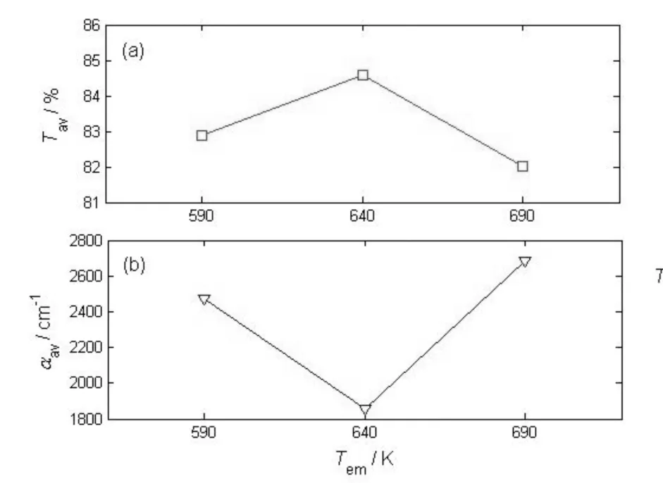
Fig.2 Influence of Tem on(a)Tav and(b)αav of the samples
Figure 3 gives the optical absorption spectra of the ZTGO samples fabricated at variousTemas a function of wavelengthλ.The absorption coefficient(α)was calculated using the equation[34]:
(2)
where OD is the optical density anddis the film thickness.The average absorption coefficient in the visible range(αav)of all the samples is plotted in Figure 2(b).Theαavvalue is observed to be very small in the visible region, indicating that the prepared samples are almost transparent in visible region.The lowest value ofαavof 1.85×103cm-1can be obtained for the thin film prepared at theTemof 640 K.
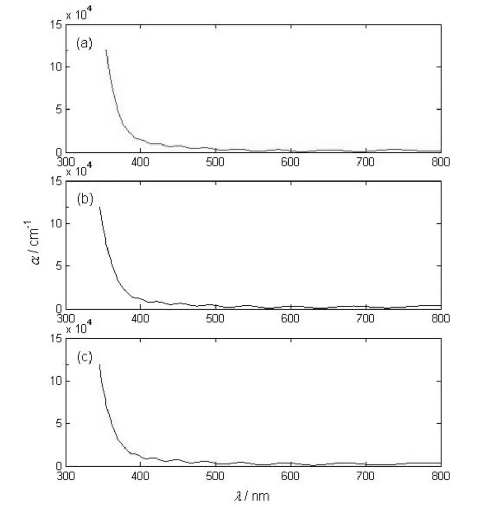
Fig.3 The optical absorption spectra of samples prepared at Tem of(a)590 K,(b)640 K and(c)690 K, respectively
At high absorption levels, the relationship betweenαandEgis expressed to calculate optical band-gap of the thin films by the following formula[35]:
αE=C(E-Eg)p,
(3)
whereE=hvis the photon energy,Cis an energy-independent constant, andpis an exponent which can assume values of 1/2, 3/2, 2 and 3 depending on the nature of the electronic transitions responsible for optical absorption.p= 1/2 and 3/2 for direct allowed and forbidden transitions, respectively,p= 2 and 3 for indirect allowed and forbidden transition, respectively.Figure 4 shows the typical Tauc plots of(αE)2versusEfor all the samples at room temperature.The values ofEgwere obtained by extrapolation of the linear portion of the graph to(αE)2= 0.A good straight line is obtained withp=1/2 for all the thin films.The optical band-gap of the prepared samples was estimated and theEgvalues are in the range of 3.41-3.51 eV, larger than that of undoped ZnO due to Burstein-Moss(B-M)shift[36].

Fig.4 The(αE)2-E curves of samples prepared at Tem of(a)590 K,(b)640 K and(c)690 K, respectively
At low absorption levels, the absorption coefficientαnear the band edge shows an exponential dependence on photon energyE, and obeys the Urbach relation[34]:
(4)
whereα0is a constant,Euis the Urbach energy, which characterizes the slope of the exponential edge.Figure 5 gives the Urbach plots of all the prepared samples.Note from the figure that lnαis shown to be linearly dependent on the photo energyαfor these thin films, indicating that the absorption processes obey Urbach's rule.The Urbach energyEuis defined as the reciprocal of the slopes of lnαversusα:
(5)
From Eq.(5), theEuvalues can be calculated out to be ranging from 0.167 eV to 0.183 eV for the prepared samples.The lowest Urbach energyEuwas obtained whenTemis 640 K which indicating a lower structural disorders of the ZTGO thin films.

Fig.5 The lnα-E curves of samples prepared at Tem of(a)590 K,(b)640 K and(c)690 K, respectively
Figure 6(a)shows the electrical conductivity(σ)of the ZTGO samples fabricated at variousTem.The values ofσare 8.11×10²S·cm-1, 7.86×10²S·cm-1and 4.87×10²S·cm-1for the samples prepared at theTemof 590 K, 640K and 690 K, respectively.Theσvalue of the thin films is observed to decrease monotonically with increasing theTem.Since there is a trade-off between the optical transmission and electrical conductivity in TCO thin films, it is important to compare the quality of TCO thin films by correlating the optical and electrical properties.In this paper, the inherent quality of TCO thin films can be quantitatively compared by using a thickness independent figure of merit(FM).It is defined as the following equation[37]:
(6)

Fig.6 Effect of Tem on(a)σ and(b)FM of the samples
whereσis the electrical conductivity,αavis the average absorption coefficient in the visible range.Figure 6(b)gives theFMvalues of the prepared samples as a function ofTem.As theTemvalue increases, the value ofFMfirstly increases and then decreases.The highestFMvalue of 0.423 S is observed for the sample deposited atTemof 640 K, which has moderateσof 7.86×10²S·cm-1, very low averageαavof about 1.85×103cm-1and high transmittance of 84.61%.The results indicate that theTemin the experiments is one of the most important factors to affect the opto-electronic performance of ZTGO thin films.
3 Conclusion
In this work,the transparent conducting ZTGO thin films were prepared by magnetron sputtering method, and the influences of the growth temperatureTemon the optical, electrical and opto-electronic performance were investigated.It is found that the temperatureTemstrongly affects the optical, electrical and opto-electronic performance of the prepared thin films.The thin film deposited at the temperatureTemof 640 K possesses the best opto-electronic performance, which have the highest average transmittance in the visible range(84.61%)and the maximum figure of merit(0.423 S).In addition, the optical band-gaps of the prepared thin films were determined and observed to be larger than that of undoped ZnO due to B-M shift.The results indicate that electrical and optical properties of the ZTGO thin films are closely related to the growth temperatureTem.