Novel DDS Based OFDM Transmitter Structure without IFFT and Interpolation Filter
Sanjun Liu,Guangming Gan
1 School of Information Engineering,Hubei Minzu University,Enshi 445000,China
2 School of physics and electronic information engineering,Hubei Engineering University,Wuhan 432003,China
Abstract: The traditional orthogonal frequency division multiplexing(OFDM)transmitter is implemented by inverse fast Fourier transform(IFFT),up-sampling and low pass shaping filter (LPSF), which occupy a large number of hardware resources and have long latency.To further meet the 5G and future 6G communication requirements,this paper proposes a novel direct digital synthesis(DDS)based OFDM transmitter structure that can replace these modules.Due to the strong parallelism of the system structure, it is very suitable for implementation on field programable gate array(FPGA)platform.After making two special simplifications to the primary structure,the refined structure becomes very simple compared with the traditional structures.Most attractively,the proposed structure has the following three advantages that i)the data transformation from frequency domain to time domain has zero latency,ii)the transformation length does not need to be an integer power of 2 and iii) the structure does not even need to use any multiplier, thus leading to low implementation complexity and high speed.Comparative experiments are carried out on Intel FPGA platform which show that our DDS based structure can save more than half of the resources compared with the traditional structures and can provide the same bit error rate (BER) performance under the condition without using any LPSF.
Keywords:OFDM;transmitter;direct digital synthesis(DDS);fast Fourier transform(FFT)
I.INTRODUCTION
OFDM has been selected as an efficient solution for high speed digital communications due to its high spectral efficiency, low complexity in dealing with large delay spread channels [1], and simple scheduling methods of radio resources.It can also effectively increase the system capacity by using multipleinput multiple-output[2].Therefore OFDM is widely used in both wireless and wire-line applications [3]and forms many communication standards, such as 802.11b and 802.11g for wireless local area network[4], digital audio broadcasting, digital terrestrial television broadcasting[5],digital subscriber loop,etc.
In traditional OFDM transmitter, the baseband signal is generated by IFFT plus interpolation shaping filtering, and then sent to digital-to-analog converter(DAC)and passed to radio frequency(RF)part of the modem.At the receiver side, after down conversion and some procedures,FFT is employed to demodulate the transmitted original data.In the whole procedure,IFFT and FFT are the most distinctive and indispensable parts of OFDM system.Until now,they seem like the unique and best way to realize OFDM transceivers ever since the method was proposed by Weinsetin and Ebert[6]in the 70’s of last century.
However, the conventional FFT (or IFFT) processors are mainly based on Cooley and Tukey’s[7]structure,thus have some adverse characteristics for implementation on FPGA platform.First, the transformed data length must be a power of 2, hence constraining the OFDM subcarriers’number to be also a power of 2.Second, they require a large number of arithmetic operations, and the hardware complexity is very high[8], which consume a lot of power and hardware resources,and may decrease system speed.Third,it always take a long operating time to achieve the transformation from the frequency domain dataX(k)to the time domain datax(n).The operating time is typically dozens of microseconds[9].
Although various sophisticated FFT processors[10,11] have been proposed, such as Vennila’s [12] dynamic partial processor and Radhouane’s[13]continuous flow mixed mode FFT architectureetc.,the abovementioned problems still exist.Therefore,if we could find a new way to implement OFDM transmitter without using IFFT,and this new structure is much simpler than the traditional architecture, it would be very attractive.Fortunately,we found a way to implement an OFDM baseband signal generator by using the direct digital synthesis(DDS)principle.
The main concept of the DDS-based OFDM transmitter is to construct all these subcarriers through DDS modules and then add all the modulated DDS signals together.By using DDS principle,the output signals in time domain are not achieved simultaneously, but are generated one by one per clock cycle when frequency domain data are available.Since the subcarriers have the same frequency spacing,only one shared memory is required for all DDS modules.In addition,because the frequency domain data in the OFDM signals always belong to the same set with finite elements, we can store the results of the multiplication operation in the memory banks in advance to avoid repeated calculations.
This paper is organized as follows.Section II briefly introduces the properties of OFDM signal and derives the main structure of the proposed DDS-based OFDM transmitter.Since the main structure proposed in this paper is very complicated, some simplified methods are provided in Section III according to the nature of the OFDM signal.Section IV implements a detailed DDS-based OFDM transmitter in the 802.11 WLAN standard according to the proposed method, and then compares it with the traditional FFT-based structure.Finally,some important features of the transmitter after the simplified structure are proposed.Section V summarizes the article.
II.ANALYSIS OF OFDM SIGNAL AND THE PRIMARY DDS BASED STRUCTURE
A brief structure of traditional OFDM transmitter is shown in Figure 1.Before the time domain baseband signals(t)is up converted and transmitted to the antenna through the power amplifier(PA),it needs to go through more than ten procedures for processing.The most distinctive and important procedures to OFDM transmitter are IFFT, up sampling and low-pass filtering in the dashed box.In this paper the proposed DDS based OFDM transmitter structure is used to replace the abovementioned three parts whose function is to convert the frequency domain dataX(k),k=0,1,...,N −1 into time domain dataS(n),n=0,1,...,NM −1, whereNis the number of subcarriers or IFFT data length,andMrepresents interpolation factor of upsampling.
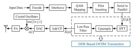
Figure 1. Replace the traditional OFDM transmitter with DDS based structure.
To understand its principle,let us consider the original definition of OFDM analog signals(t)in time domain.Suppose the OFDM symbol’s period isTwithout cyclic prefix(CP),then the first subcarrier’s analog frequency isf1=,and

Sinces(t)is generated by the digital-to-analog convertor(DAC)whose sampling interval isand sampling frequency is

the expression ofS(n)in Figure 1 can be obtained by substitutingt=into(1),i.e.,
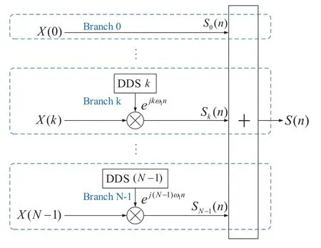
Figure 2. The primary structure of DDS based OFDM transmitter.

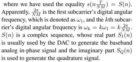
As indicated in (1) and (3), both the analog and digital OFDM signals are created by adding a number of modulated subcarriers together.It is challenging to create analog sub-carriers through analog methods,but it is easy to construct these digital sub-carriers through DDS principle in FPGA platform.Without considering the implementation complexity, the primary structure of DDS based OFDM transmitter implemented by FPGA platform is shown in Figure 2.
In Figure 2, there areNbranches, each of which contains a complex exponential DDS module and a complex multiplier denoted as the symbol “⊗”.Thekth DDS module is used to stream out the complex exponential signal exp(jωkn) on thenth rising edge of clock cycle, wheren= 0,1,...,NM −1.Therefore,each branch can output a complex number at every system clock.The data output by thekth branch at thenth clock cycle isSk(n) =X(k)exp(jkω1n).The symbol“+”represents a multiple input single output(MISO)complex adder,which can sum upSk(n),i.e.,S(n)=
It is noted that there is trivial difference between the conventional DDS module and the proposed complex exponential DDS module.The former one normally outputs real sine signal, and the latter one outputs complex exponential signal which contains two sine sequences with 90 degrees phase shift.In practice, we can implement the proposed complex exponential DDS module by combining two conventional DDS modules together, one module generating the real part and the other generating the imaginary part.For detailed understanding of DDS principle,see article[14]and the subsections A and B in section III of this article.
Although Figure 2 looks very complicated, in the next section,we will introduce some special methods to simplify the structure,making it more effective and simpler than traditional OFDM transmitters.
III.SIMPLIFICATIONS FOR THE PRIMARY STRUCTURE
Figure 2 is complicated because it consists ofN −1 complex multipliers andN −1 complex exponential DDS modules.Each DDS module uses two memory banks to store thesinrotation factor sinandcosinerotation factor cos[15]respectively forn= 0,1,··· ,NM −1.This means that the structure of Figure 2 requires a large number of memories and multipliers.However,since the digital angular frequencies of DDS modules are increased by the same time frequency interval,all DDS modules can share a common memory bank.In addition,all the frequency domain dataX(k),k= 0,1,...,N −1 belong to the same set of finite elements, so the multipliers can be omitted and replaced with some easy-to-implement selectors.Based on these points,this section introduces three detailed simplification stages and their implementations to the primary structure in Figure 2.
3.1 Simplification Stage 1: Sine and Cosine DDS Modules in A Branch Share A Common Memory Bank
Expending the complex multiplication of thekth branch in equation (3), the detailed expression ofSk(n)is

where the suffix “I” and “Q” represent in-phase part and quadrature part of a complex signal respectively.We can find from equation (4) that bothSkI(n) andSkQ(n)require two traditional DDS modules to generate the sine and cosine sequences respectively.But in fact,the sine and cosine sequences have the same digital angular frequencyωk=which determines that they can be generated by fetching the data from a common memory bank.Assuming a memory bank stores the sequence sin(ωkn),n= 0,1,...,−1 for a whole period of sine,if we fetch the data one by one from the beginning of the bank, then we can get sin(ωkn).However, if we fetch data from the indexin the bank, namely it is 90 degrees phase shift from the first element,then we can get cos(ωkn).Finally,by using a common memory bank,the structure of thekth branch is simplified in Figure 3.
In Figure 3, the complex multiplier is replaced by four real multipliers which are located in four subbranches, each of which refers to a term in equation(4).There are two real adders that are respectively used to calculate the in-phase and quadrature part ofSk(n).The symbol “-1” means that the product ofXQ(k)and sin(ωkn)should multiply−1 before entering the first adder.Although the proposed simplification stage 1 can save the memory consumption to half of the primary structure, it seems still complicated.This issue can be further optimized by the following two stages.
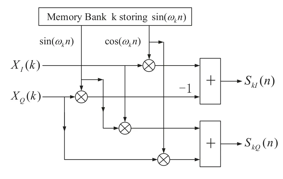
Figure 3. Schematic of simplification scheme 1 that two DDS modules in kth branch share a common memory bank.
3.2 Simplification Stage 2: All DDS Modules Share A Common Memory Bank
In Figure 2, although each branch requires its DDS module to output a different digital angular frequency data sequence,all these digital angular frequencies are integer multiples of the first branch.The digital angular frequency of the first branch isω1, and thek’s branch iskω1.By using this property that exclusively belongs to OFDM,we can make all the DDS modules share a common memory bank that stores a whole period of sine signal with digital angular frequencyω1.Figure 4 demonstrates a schematic example for three DDS modules that share a common memory bank and stream out their data sequences with respective digital angular frequencies ofand.
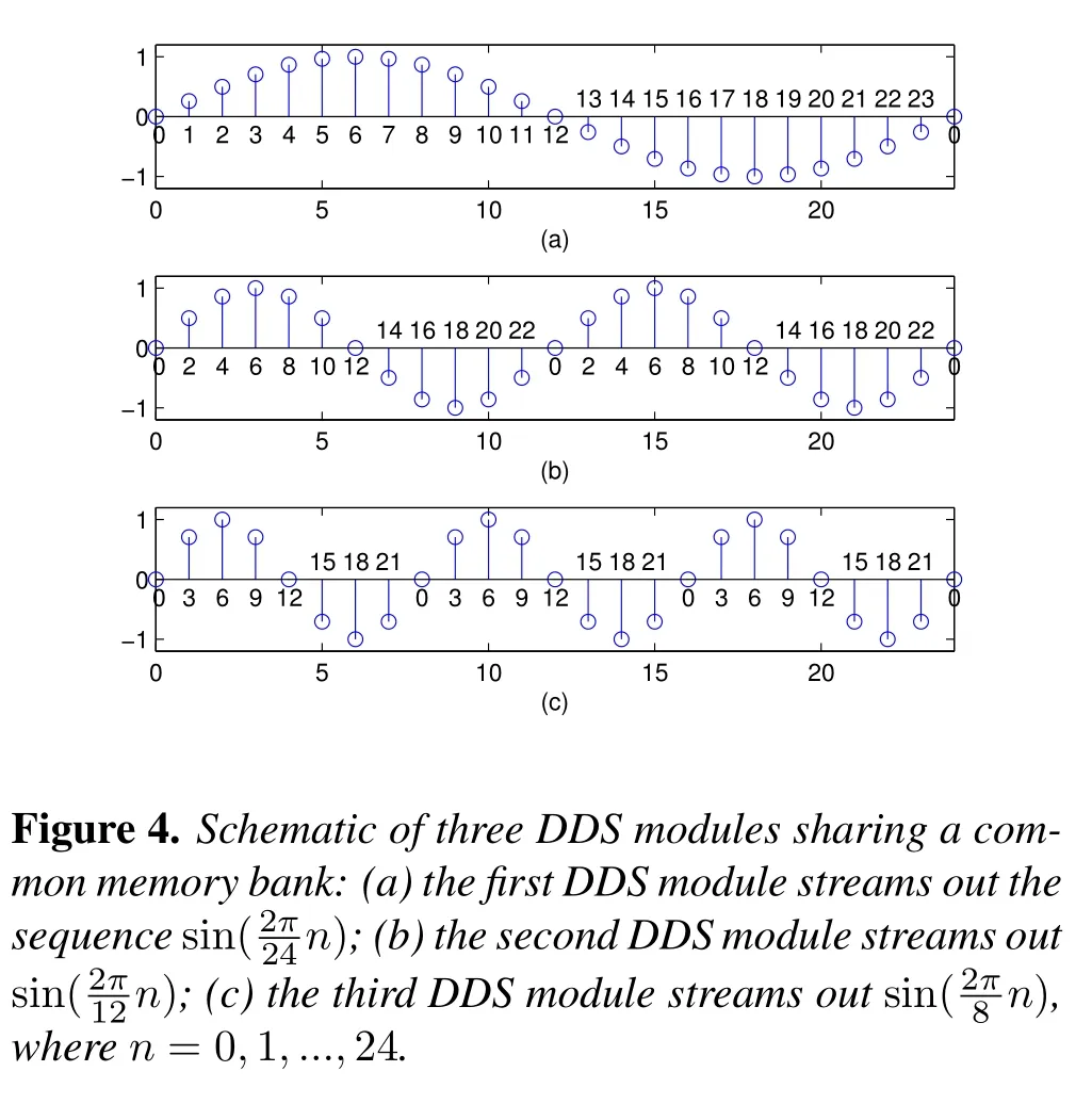
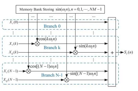
Figure 5. Simplified structure of OFDM transmitter by using both stages 1 and 2,Note: the quadrature part has the same structure which is omitted.
To generate DDS signals with different digital angular frequencies by using a common memory bank we should pre-store the data sequence sinn=0,1,··· ,23 in a memory bank as depicted in Figure 4(a).If we repeatedly fetch the data from the bank one by one at every rising edge of the clock,then the outputsinsequence is sinn= 0,1,··· ,∞, i.e.,its digital angular frequency isIf we fetch one data from every two data in the bank as depicted in(b),i.e.,repeatedly fetch the data with indexes 0,2,4,··· ,22,then the sine sequence sinn=0,1,··· ,∞can be obtained.Its digital angular frequency is,which is twice ofω1.By the same approach that fetches one data from every three, we can get the digital angular frequency,which is tripleω1.
If the digital angular frequencyω1in (a) is called“base frequency”,according to the proposed approach,then we can obtain any desired digital frequencies that are integer multiples of the base frequency as long as we fetch the data at difference intervals.Supposing the sampled data number in a whole sine period isNs,then the digital angular frequency is

Furthermore, by this approach it is convenient to generate the DDS signals with optional initial phases,as long as we fetch data from the right locations in the bank.Especially if we want to generate a “cos”or “−sin” signal, and so on, we can fetch data from one quarter or half of the bank,etc.It is worth noting that there exists an modulo operating in the repeatedly fetching data procedure,i.e.,if we fetch the data close to the end of the bank, and the next data’s index will exceedNs, we should subtract the index byNs, and pick the data from the new index.Combining the approach mentioned above and method 1,the structure of OFDM transmitter can be strongly simplified as shown in Figure 5,where for ease of demonstration,we only depict the implementation ofSI(n), whileSQ(n) is omitted because of its similarity.
In Figure 5 we use only one memory bank to generate DDS sequences for all theNbranches.Each branch contains two sub-branches, which fetches one data from the memory bank at every rising edge of system clock and calculateXI(k)[cos(kω1n)] andXQ(k)[−sin(kω1n)] respectively at thenth clock cycle for thekth branch.The memory bank totally storesNMdata whose expression is

In thekth branch, each sub-branch fetches data at the interval ofk, then its digital angular frequency isIn this process,we do not really realize any analog DDS signal, but by using the DDS principle,these digital subcarrier signals are ideal.Because the 0th branch’s digital angular frequency is 0, its output degenerates to constantXI(0).The structure in Figure 5 still contains multipliers which is not desired.In next section the third simplification approach is used to discard all of them.
3.3 Simplification Stage 3: Remove Multipliers by Pre-storing Products
To remove the multipliers in Figure 5, we should first explore what they have done.Note that each sub-branch contains a multiplier, and each multiplier have two input data, i.e., the frequency domain dataXI(k)orXQ(k)and the subcarrier’s data cos(kω1n)or−sin(kω1n).Usually,XI(k) andXQ(k) belong to the same set with finite elements.For convenience,we denote the set as “modulation set”.For example,in the QPSK modulation,XI(k),XQ(k)∈{1,−1};in the 16QAM, the modulation set is{3,1,−1,−3},etc.In addition, each subcarrier’s data are from the shared memory bank as shown in Figure 5.That is to say,both the two data input to each multiplier belong to their respective fixed sets, so that these multipliers do a lot of duplicated works.Hence there is no need to compute these data’s products repeatedly.Instead,we can pre-store these products in some memory banks,and then fetch the right data from the related bank.According to this method,these multipliers can be discarded and replaced by selectors.
For ease of demonstration, Figure 6 only depicted the implementation ofSI(n), the quadrature partSQ(n) can be realized in the same way.In Figure 6,each sub-branch uses a selector to replace the multiplier in Figure 5,and to fetch data from one ofRmemory banks,whereRequals the number of different absolute values of those elements in the modulation set.The smallerRis,the fewer memory banks are needed.Fortunately,Ris usually very small in the lower order QAM modulation.Assume the OFDM transmitter is usingxQAM,herex=4y,then
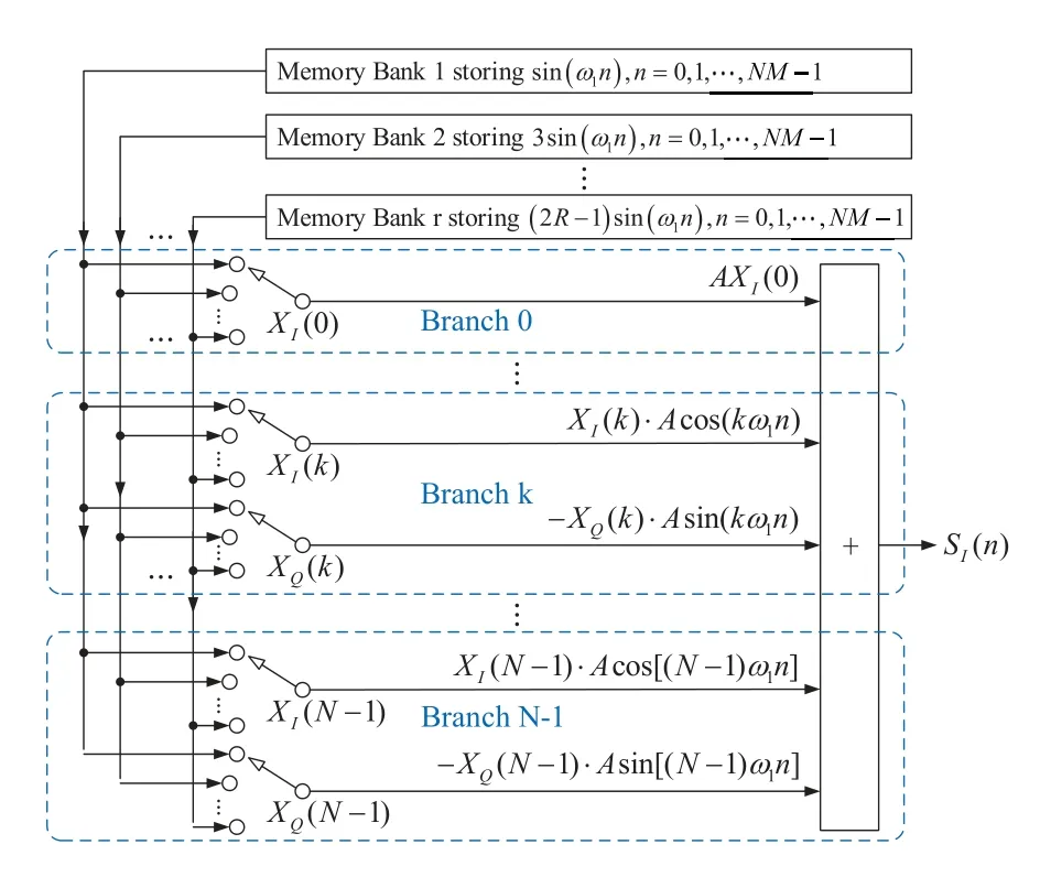
Figure 6. Simplified structure of OFDM transmitter that uses selectors to replace multipliers, Note: the quadrature part has the same structure which is omitted.

For example, in QPSK (similar with 4QAM),R=1;in 16QAM,R= 2;in 64QAM,R= 4,and so on.Because these absolute values of the elements in the modulation set equal to 2r−1,r=1,2,...,R,thereby,therth memory bank has data sequence expression

The proposed structure works as follows.When the OFDM transmitter is powered on, the system starts to generate clock pulses.The frequency of the clock pulse is equal to the sampling frequency of the DAC,i.e.,.At the first rising edge of clock tick, every selector in Figure 6 begins to fetch data from a certain memory bank according to the sub-branch’s|XI(k)|(or|XQ(k)|).If|XI(k)|or|XQ(k)|= 2r −1,wherer= 1,2,...,R, then the sub-branch should fetch all the data inrth memory bank from the right initial phase and at the right interval.Every branch contains four sub-branches,and each sub-branch is used to calculate one of the four terms in equation(4).The structure of each term can be summarized as

where|XIQ(k)|representXI(k) orXQ(k),sincosrefers tosinorcos, andsignstands for its sign.For example, if one sub-branch calculates−XQ(k)sin(ωkn) andXQ(k) =−3, thensign=+,|XIQ(k)|=3 andsincos=sin.
According to the value ofsignandsincos,each sub-branch should fetch data at the following four initial phases.If one sub-branch calculates“+|XIQ(k)|sin(ωkn)”,it should fetch data from 0th element in the memory bank; if the sub-branch calculates “+|XIQ(k)|cos(ωkn)”, it should fetch data fromth element in the memory bank, meaning 90 degrees apart from the 0th element; if the subbranch calculates “−|XIQ(k)|sin(ωkn)”, it should fetch data fromth element in the bank, meaning 180 degrees apart; if the sub-branch calculates“−|XIQ(k)|cos(ωkn)”, it should fetch data fromth element in the bank, and this is 270 degrees apart from the 0th element.Once the memory bank’s index and the original phase is fixed, then at every rising edge of clock tick each sub-branch in thekth branch fetch a data from its selected bank at the interval ofk.If one sub-branch is going to fetch the data with the index overNM −1, the sub-branch should perform a modulo operation for the position as mentioned previously.Meanwhile, the two MISO adders can sum up all these in-phase data to formSI(n)and quadrature data to formSQ(n) respectively in one clock periodBased on the structure in Figure 6, the next section will introduce the detailed implementation of the proposed OFDM transmitter.
IV.COMPARISONS OF EXPERIMENTAL RESULTS AND SOME FEATURES
This section take the IEEE 802.11a standard baseband signal as example to realize OFDM transmitters on FPGA platform.Comparisons between the traditional and the proposed structure are carried out, including how to add cyclic prefix (CP), the spectral analysis,the computational complexity, and their hardware resource consumptions.
4.1 Implement IEEE 802.11a Baseband OFDM Transmitter
In the traditional OFDM transmitter, the basic architecture consists of three parts: the IFFT block, the upsampling interpolator and low pass shaping filter.However,in the proposed structure,all these parts are not needed,instead,we use some basic materials that are close to gate level and easy to make,i.e.,Rmemory banks,4N −2 selectors and two MISO adders,as depicted in Figure 6.After computing these parameters for the implementation,we will especially survey the way to add CP.
In the IEEE 802.11a standard [16], there areN=64 subcarriers,each of which has the frequency intervalf1= 312.5KHz.The period of OFDM symbol without CP isT== 3.2×10⁻⁶s.Suppose the interpolation factor isM= 4, the DAC’s operating frequency,or the frequency of system clock can be expressed as

In IEEE 802.11a standard, 16QAM modulation is used,then according to equation(7)

which means that the transmitter needs only two memory banks to pre-store the data sequencesand 3respectively,wheren= 0,1,...,255.Suppose each data in the memory bank is denoted as an 8 bit signed integer,the proposed structure is composed of two memory banks that consumes total 512 bytes,254 selectors and two adders each of which has 127 inputs and one output.Finally,by using these parameters and adding the quadrature partSQ(n)to Figure 6, we can implement the proposed OFDM transmitter.
4.2 Novel Scheme to Add CP
In the OFDM communication system,CP(also called guard interval)must be added to combat multipath.In addition to the traditional copying and pasting method to add CP,in the proposed DDS based architecture we can also add CP by the following method.Note that if we substituten=n+NMinto equation(3),then
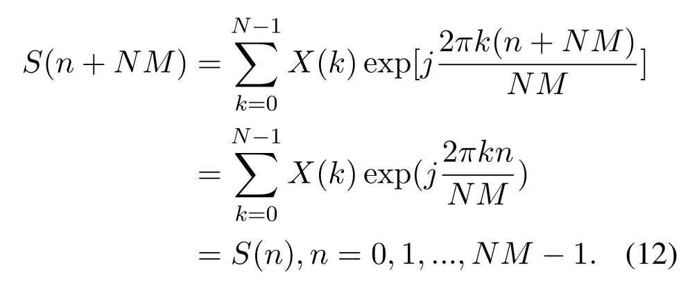
This means that the proposed structure can repeatedly output the sequenceS(n) with the period ofNMclock cycles, as long as all the sub-branches continuously operate and the frequency domain dataX(k),k= 0,1,...,N −1 are retained.Therefore, if we want to add CP of a certain length,for example,Ncsampling points, we just need to let the system continue to work withNcsampling points and keepX(k)unchanged.
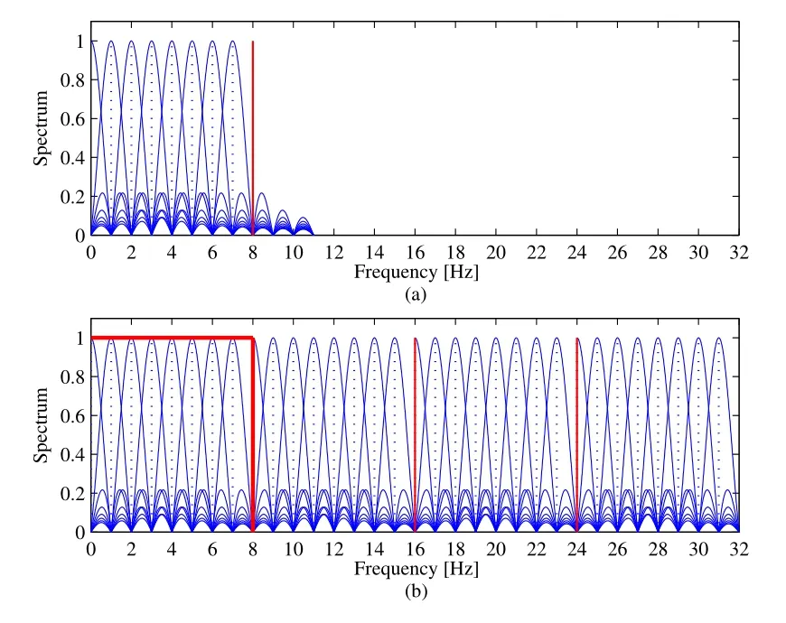
Figure 7. Spectrum comparison between the proposed and traditional OFDM transmitter: (a) spectrum of proposed structure which is naturally constrained in baseband; (b)spectrum after traditional process of upsampling and inserting zero in traditional structure.
4.3 Spectrum Analysis
By expanding equation (3) to infinite OFDM symbols, it is easy to derive its frequency domain formula.Suppose the OFDM symbol’s index isp,wherep ∈{−∞,...,−1,0,1,...,+∞}.The expanded equation(3)can be expressed as
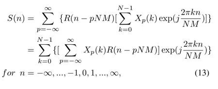
whereR(n −pNM) is the rectangle function, and whenpNM ≤n ≤(p+1)NM −1,R(n−pNM)=1, elseR(n −pNM) = 0;Xp(k) represents thekth branch’s frequency domain data in thepth OFDM symbol.
From equation (13), we can obtain the data sequence output from thekth branch isSk(n) =[Xp(k)R(n −pNM)]}exp,n=−∞,...,−1,0,1,...,∞.This denotes that in thekth branch, its baseband signal varies with periodic dur ation ofNMclock cycles, and the baseband signal is modulated by digital angular frequencymeaning its spectrum is moved from origin tofore,if discrete Fourier transform(DFT)is applied to equation(13),then the spectrum picture can be shown in Figure 7(a),where theNsubcarriers are evenly distributed in the frequency span[0,Nf1].Here,for ease of comparison, the spectrum after the process of upsampling and inserting zero by traditional IFFT based OFDM structure is depicted in 7(b).In both Figure 7(a)and(b),we setN=8,M=4,andf1=1Hz.
In Figure 7(b),because the baseband spectrum is repeatedMtimes,a LPSF must be used to filter out the low-frequency part, so as to generate the signal that can be sent to the DAC.Because the repeated spectrum is very close to the desired baseband spectrum,how to design a low complexity and efficient LPSF so that to retain the low frequency baseband spectrum is challenging [17].However in the proposed DDS based structure,most of the spectrum is naturally constrained in the low frequency band, and the out-offband spectrum has very low power ratio relative to inband spectrum, because only those marginal subcarriers have some sidelobes outside the specified bandwidth.In the sense of having maximum similarity with the original definition of analog OFDM signal in equa-Theretion(1),the out-off-band spectrum is indispensable.It is noted that the issue of out-of-band power leakage has been investigated and addressed in[18,19].In addition,the proposed structure does not reject low pass filter.If we want to constrain the spectrum in a specified low bandwidth,we can add a low pass filter after the structure.
4.4 Waveform and BER Comparisons
This subsection shows the time-domain waveform generated by the proposed method as well as the bit error rate (BER) comparison with that of the traditional IFFT based method, so as to give readers an intuitive feeling about its shape and performance.Because the development tools of FPGA, such as Quartus and Modelsim, can not make two waveforms display together, and the calculation results of various schemes have nothing to do with the choice of development tools,so we use matlab to calculate the waveform data in equation (3) and show the waveform in Figure 8.
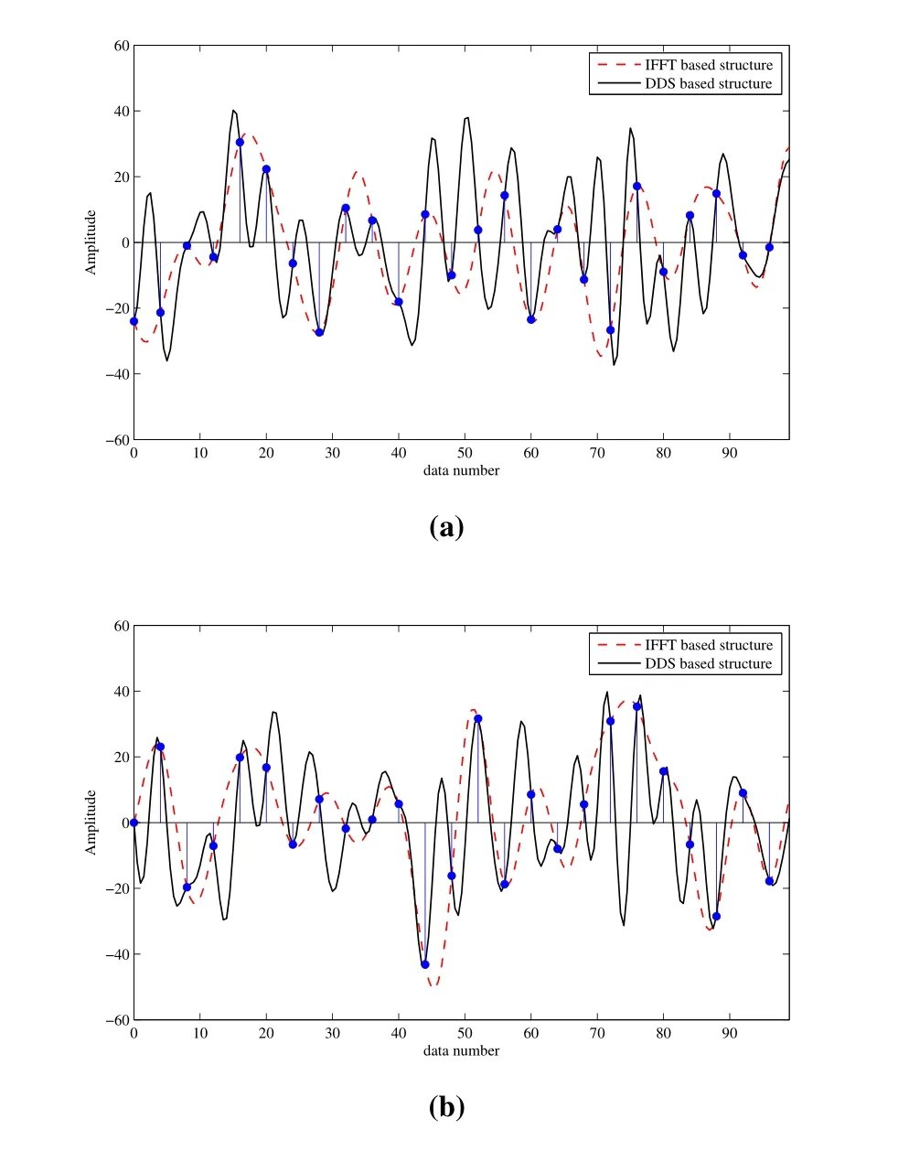
Figure 8. Waveform of the in-phase part and quadrature part of OFDM baseband signal by the proposed DDS based method and the traditional method,where(a)is the in-phase wave and(b)is the quadrature part.
In Figure 8,the system setting is the same as stated in subsection A of this chapter, that is, the subcarrier’s numberN= 64, interpolation factorM= 4.So that the total number of the time domain baseband data is 256.However we only show 100 points for the purpose that to display the details more clearly.We use a 41 order raised cosine filter for shaping filtering in the traditional IFFT based structure, but we do not use any filter for band limiting in our proposed scheme.It can be seen that although the waveform generated by our DDS based scheme does not overlap with that of the traditional method, these points whose data number is integer multiple ofMhave the same value with each other, and these values are exactly equal to the IFFT ofX(k)which are represented by blue stems.This phenomenon can be proved as follows.Letn=mM,m= 0,1,··· ,N −1, and substitute it into equation(3),then
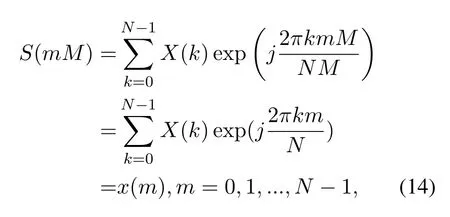
wherex(m) is the IFFT ifX(k).The derivation of equation(14)shows that the extracted signalS(mM)fromS(n)does not change withM.In addition,this reveals that in the DDS based methodS(n) is generated by being directly interpolated fromx(m).This explains why we can omit the interpolation module in our structure.
The profile of BER versus signal to noise ratio(SNR) is shown in Figure 9 which demonstrates that our DDS based scheme can provide nearly the same performance as that of the traditional scheme.The BER of the proposed scheme decreases with the increase of SNR.When the SNR reaches 20dB,the BER is decreased to less than 10−5.5.The simulation scenarios used by the two schemes are the same as those mentioned above.The BER is obtained at the situation that we did not use any channel coding scheme in the simulation.If channel coding scheme such as turbo is used in the system,lower BER can be reached.
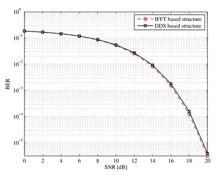
Figure 9. BER comparison between the proposed and traditional OFDM transmitter.
4.5 Experimental Results on FPGA Platform
The comparison experiment is carried out on the FPGA platform DE2[20].The platform uses Cyclone II EP2C35 FPGA chip with 483840 memory bits and 33216 logic elements (LEs).The hardware complexity of our proposed structure mainly comprises two 256-byte memory banks and two MISO adders as described in Section 4.1, while the traditional OFDM transmitter is implemented by a 64-point IFFT module, an upsampling module and a 41-tap low pass filter.We use two ways to realize the IFFT module re-spectively.One way is by Quartus II MegaCore, the other way employs Mahdavi’s algorithm[21]available of high speed, high resolution and low latency.Both of them realize 64 point IFFT.
The comparative parameters of these methods are mainly hardware consumption (HC) and latency.HC comprises dedicated multipliers (Mults), logic elements (LEs)and memories(Mems).Latency is measured by the clock number consumed during the data transformation fromX(k),k= 0,1,··· ,N −1 being ready toS(0) being outputting.All these parameters can be provided by Quartus II development tool,which are shown in Table 1.
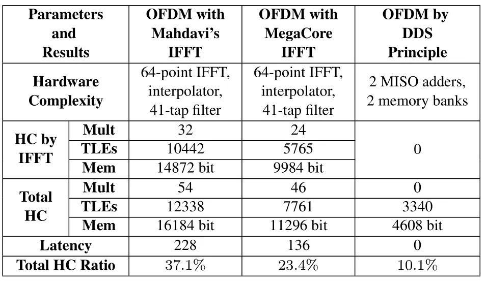
Table 1. Performance comparisons of the experiment.
According to the data in Table 1, it is proved that our OFDM transmitter structure requires less hardware resources and have less latency.This is due to the fact that the proposed structure does not need to use multipliers and has much simpler controlling logic than the traditional structure.In the proposed structure, the controlling logic is accomplished by selectors,and they just need to repeatedly fetch data from a fixed memory bank at a constant interval,thus leading to low implementation complexity.In contrast with the case of IFFT, the structure is always divided into many stages,in which those data is multiplied by different twiddle factors.How to find the right factors is a complicated issue.Moreover, IFFT module normally needs a reordering procedure to adjust the data sequence, which need additional resources and clock cycles.It is amazing that our OFDM transmitter has zero clock cycle latency.This is because the system has high parallelism, that is, each branch can fetch a data in the same clock cycle, and meanwhile, the MISO adders can sum up all these data in only one clock cycle.
V.CONCLUSIONS
A novel OFDM transmitter based on DDS principle has been presented and implemented on FPGA platform.In the proposed structure, because all the subcarriers work in parallel at the same time, the system architecture is particularly suitable for FPGA platform which is of strong parallel ability.By making full use of OFDM signal’s two unique nature, the proposed structure that is realized on FPGA platform is greatly simplified,so that the hardware usage has been saved by more than 50%compared with the traditional structure.The most attractive attribute is that the proposed OFDM transmitter has zero latency in obtaining the first time domain dataS(0) from the frequency domain dataX(k).Because our method is a new simple way to realize OFDM digital sequences,and does not change the format of OFDM signal,the characteristics of OFDM signal,including timing synchronization deviation offset,phase offset,frequency offset and the BER, are the same as those of traditional OFDM signal.Special to note is that we have no idea to apply the similar scheme to the receiver and simplify its structure, because the received signal in the receiver is not constrained to a specific limited set with very few elements as the“modulation set”in the transmitter.Relevant literature has not been found.
ACKNOWLEDGEMENT
This work was supported by the Natural Science Foundation of Hubei Province under Grant 2019CFB593,National Natural Science Foundation of China under Grant 61961016, and Starting Fund for Doctoral Research in Hubei Minzu University under Grant MY2018B018.
- China Communications的其它文章
- An Overview of Wireless Communication Technology Using Deep Learning
- Relay-Assisted Secure Short-Packet Transmission in Cognitive IoT with Spectrum Sensing
- Frequency-Hopping Frequency Reconnaissance and Prediction for Non-cooperative Communication Network
- Passive Localization of Multiple Sources Using Joint RSS and AOA Measurements in Spectrum Sharing System
- Specific Emitter Identification for IoT Devices Based on Deep Residual Shrinkage Networks
- Primary User Adversarial Attacks on Deep Learning-Based Spectrum Sensing and the Defense Method

