Review of Power Decoupling Methods for Micro-Inverters Used in PV Systems
(School of Electrical Engineering and Automation, East China Jiaotong University, Nanchang 330013, China)
Abstract: In single-phase photovoltaic(PV) systems, power mismatch between input and output terminal leads to power pulsation, seriously affecting maximum power point tracking (MPPT). Paralleling an electrolytic capacitor(e-cap) across the PV panel to smooth power pulsation seems to be an unreliable method owing to its short lifespan. Various power decoupling methods used in micro-inverters have been proposed to solve the problem. These methods were categorized. Some of them were introduced in this paper regarding efficiency,cost and technical features. Special novel methods proposed in recent years were presented to show the development trend of micro-inverter. Then, conclusion and comparisons were made. Finally, a potential technological route was proposed by author for further study on power decoupling.
Keywords: Photovoltaic, micro-inverter, power decoupling, MPPT.
1 Introduction
With the PV market developing rapidly, it is predicted that global installed capacity of solar electric energy will reach a height of 700GW in 2020[1]. A micro-inverter, which plays an important role in integrated PV building, contributes to PV market development.
For a micro-inverter, there are many advantages:①High efficiency; ②Ease of expandability; ③Plug and play; ④Space saving; ⑤High reliability and so on.In a grid-tied micro-inverter system(GTMIS), the grid line is single phase connected. However, it has an obvious shortcoming in that the input power is constant while the power following to grid is time varing with a double-line-frequency oscillation in single phase system[2-3]. Usually, a large e-cap, as a decoupling element, is employed across PV panel to handle power pulsation caused by the differential power between input and output terminal of single phase system.Although many advantages are presented above, it still cannot satisfy the reliability requirements for a GTMIS[4]. Because the e-cap easily degrades due to its electrolyte loss with time[5], it has a typical lifespan of 1000~7000 hours at 105°C operating temperature. That is not enough to meet the lifetime of semiconductors. It is widely known that many semiconductor devices are featured by long lifetime in a GTMIS. As reported, the low power switches can operate at least 10,000 hours while PV panels warranted to 25 years of operation are routinely available[6-7].
The problem mentioned above only exists in a single phase GTMIS. Three-phase GTMIS satisfy power balance naturally, thus decoupling capacitors can be omitted. However, three-phase GTMIS is not normally applied in small power applications less than 10kW subject to its cost, volume, etc. Limited by present technologies, research on long-life e-cap remains stagnant. Research on low voltage long-life e-caps encounter great challenges because of hydrated reaction.Developing power decoupling techniques without e-cap in micro-inverter becomes the research hotspot[8-11]. By using power decoupling techniques, micro-inverters can handle power pulsation and substitute reliable long-life film capacitors for e-caps. Various power decoupling methods for micro-inverts are presented by many researchers. Moreover, power decoupling technique is commonly used in light-emitting-diode(LED) lighting applications[12]. A review of decoupling methods for micro-inverters is required to introduce research progress in this area. This paper is organized as follows:the concept of power decoupling is discussed in Section 2. Many typical methods are introduced in Section 3 with comparison in Section 4. Section 5 proposes a potential technological route by author for further research. The conclusion is made in Section 6.
2 Principle of power decoupling
PV panel should operate at constant maximum power point(MPP) for maximizing energy harvest.Generated powerPPVfrom PV panel is given by

WhereUPVandIPVare the voltage and current of PV panel.
The injected current to the grid,i(t) and the grid voltage,u(t) are given by

whereUandIare the amplitude of grid voltage and injected current respectively,ωandφare the grid frequency and power factor angle respectively.
The instantaneous output powerPaccan be expressed as

Assuming no phase shift, (3) can be rewritten as

where,Pav=UI/2,Pav(2ωt)=Pavcos(2ωt). The instantaneous power in (4) consists of two terms as shown in Fig.1. The average powerPav, is the average value of the output power and the second termPavcos(2ωt) is a time varying power with twice the grid frequency. If power loss in the inverter is ignored,Pavwill be equal toPpv. The time varying power will cause current ripple in the PV side. It not only disturbs MPPT process, but also distorts current injected to grid.
In order to solve these problems, power decoupling circuit should be employed as a buffer to handle power pulsation. Under certain conditions, the PV cell can be regarded as current source and current fluctuation decreases the energy harvest significantly[13]. Usually, a capacitor is placed in parallel with PV module. Then,power pulsation is transferred to the capacitor in the form of voltage ripple, in which large current fluctuation in the PV side is avoided. Required decoupling capacitance is given by

WhereUavand ΔUare the average voltage and the allowed peak-to-peak voltage variation across the capacitor.
Decoupling capacitance can be reduced by increasingUavor ΔUas shown in Fig.2, providing probability for using long-life film capacitor.
3 Power decoupling methods
By using power decoupling methods, the lifespan of inverter and PV utilization factor can be increased and in power decoupling circuit film capacitor plays a critical role. Although this technology brings some advantages, additional loss of decoupling circuit should not be ignored. Besides, cost and control complexity merit consideration. It is noteworthy that selected power decoupling method usually depends on special micro-inverters topologies. This feature contributes to classification study on power decoupling.
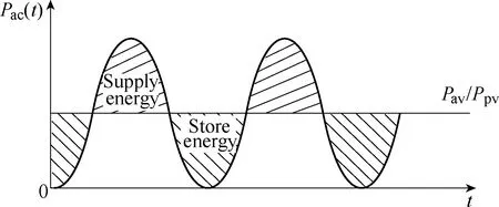
Fig.1 Instantaneous output power with power pulsation processed by decoupling capacitor

Fig.2 Required capacitance value when Ppv=200W
3.1 PV side decoupling
This decoupling method can be further categorized into two types: series PV side decoupling topologies are usually used in current source inverters(CSI), in which bulky inductor slows down dynamic performance;Micro-inverters with shunt PV side decoupling topologies,which can be operated in discontinuous-conduction mode (DCM), are more widely used.
The topology shown in Fig.3 is a flyback-type micro-inverter with power decoupling circuit[14]whose structure is similar to active clamp circuit while operation principle is not. The decoupling circuit only uses a 40μF film capacitor and a switch for a rated 100W inverter. S1keeps on until primary winding current reaches fixed value in each switching cycle to maintain input power constant. Primary winding is magnetized and then, magnetizing energy is released to decoupling capacitorCDtotally. Finally, this part of energy is controlled so as to generate required amplitude of magnetizing current on the primary winding and to release the current from the second side, namely,sequence magnetizing method(SMM). In this design,leakage inductance energy can’t be recycled and decoupling circuit handles all the PV power, which results in significant loss. The peak efficiency reported is only 70%.
Hu[15]proposed a modified topology with power decoupling circuit as shown in Fig.4, where an extra diode D1is used compared to the power decoupling topology in Fig.3. Similar to [14], S1keeps on until primary winding current reaches reference value to maintain input power constant during the first stage of a switching cycle. However, during the next stage, primary inductor releases its surplus energy or attracts part of the energy from the decoupling capacitor, CD, in order to inject required energy to grid. In this design, the peak efficiency reaches 90.23% for a 100W system.
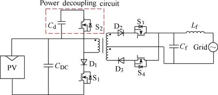
Fig.3 Topology proposed by Shimizu, et al[14]
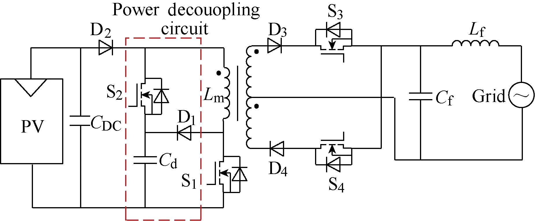
Fig.4 Topology proposed by Hu, et al[15]
Li[16]proposed a topology as shown in Fig.5. This inverter has an extra inductor,Ld, on decoupling circuit.It works as a boost converter when the decoupling capacitor is charging. In this way, higher voltage across the capacitor is attained. Consequently, e-cap is removed and the PV panel performance is not affected. However,reference values ofILdandILmboth vary with time,complicating control.
By introducing the concept of active power filter,Kyritsis[17]proposed a topology with a bidirectional buck-boost circuit as shown in Fig.6, whereIPAFis controlled to flow given reference value by using current hysteresis control. Thus, PV current with double-line frequency is smoothed for higher PV utilization factor.However, in this design, the amount of pulsated power handled by decoupling circuit is a bit larger than that handled in [16], which increases the required decoupling capacitance. Voltage ripple of decoupling capacitor can’t be too large so as to deteriorate system efficiency, in which case a 500μF capacitor is used in a 70W inverter design.
3.2 DC-link decoupling
In multi-stage inverters, the independent power stage is optional to realize MPPT. To implement power decoupling, a decoupling circuit like topologies presented in part A is not needed because a capacitor is enough. As expressed in Eq.(5), increasing average voltage and voltage ripple across capacitor contributes to reduce decoupling capacitor capacitance. There is no doubt that placing a capacitor in parallel with DC link allowing required high voltage ripple is an alternative.However, high voltage ripple may cause deterioration of current injected to grid. This type of method increases efficiency by eliminating additional loss resulting from decoupling topology by using special control algorithms,however, its stability and reliability require rigorous test.
Brekken[18]proposed a control strategy as shown in Fig.7 that allows voltage ripple (peak to peak 25%). In this design, the front-end converter extracts ripple-free power from the array and a high-bandwidth AC current loop in the inverter ensures that DC voltage ripple dose not distorted AC output current. Designed voltage loop cutoff frequency is set at just 10Hz, in which case double-line-frequency is clearly attenuated while transient response of system is decreased.

Fig.5 Topology proposed by Li, et al[16 ]
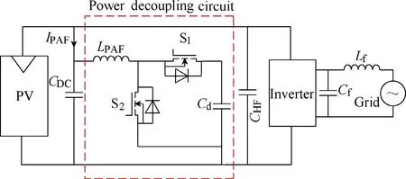
Fig.6 Topology proposed by Kyritsis, et al[17]
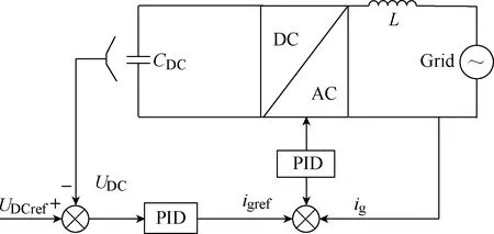
Fig.7 Control strategy proposed by Brekken, et al[18]
Fig.8 illustrates another control strategy proposed by Rodriguez[19]. The design depends on a three-stage topology where VCCS is controlled by the first stage circuit(not shown in Fig.8), which introduces soft switching technology to reduce switching loss. In this method, output current controlled by a D flip-flop implies current hysteresis is employed to generate current that follows a rectified sine wave. Low pass filter(LPF) in voltage loop also reduces dynamic performance.
To solve this problem, Kotsopoulos[20]proposed a method to predict the inverter power required to correct a DC voltage error within one fundamental AC cycle,which still required much time to overcome input power or DC-link voltage disturbance. The authors of [21]proposed an effective control scheme as shown in Fig.9 where an estimated DC-link voltage ripple is compared with the actual measured quantity. The resultant ripple-free signal is used to generate the reference current for grid injection. In the design, bandwidth for the voltage loop is broadened to acquire good behavior.
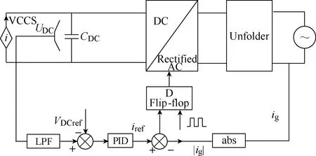
Fig.8 Control strategy proposed by Rodriguez, et al[19]
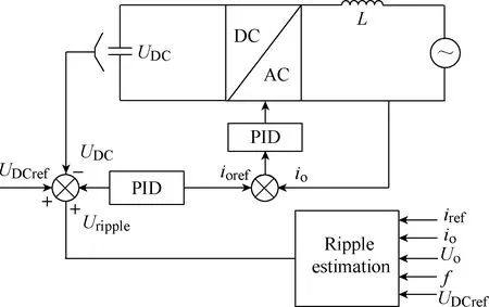
Fig.9 Control strategy proposed by Ninad, et al[21]
3.3 AC side decoupling
Given the reference [22-24], AC side decoupling featured by sophisticated control methods depend on micro-inverter with full-bridge structure, in which decoupling capacitor is usually embedded in the inverter stage itself. Decoupling capacitance can be reduced owing to large voltage fluctuated at AC side, but high voltage stress in power switching will lead to much loss.Two AC decoupling methods are illustrated in following figures, where bidirectional switches are used to provide closed loop for decoupling energy.
A CSI with power decoupling circuit is proposed by Bush and Wang[22]as shown in Fig.10, where an additional leg b is added to the ac-side to connect a capacitor between inverter and grid while other two legs a and c of the bridge are connected to grid through a CL filter. Control ofibis the critical technique for maintaining the instantaneous power flow across the converter bridge to be constant. In this manner, the concept of space vector is used to determine the amplitude and phase of leg b current,ib.
Chen[23]proposed a voltage source inverter with power decoupling topology as shown in Fig.11 where decoupling capacitor is replaced by a small inductorLb.Control strategies for these two topologies are similar.
3.4 Other decoupling methods
Many novel decoupling methods[25-33]have been proposed in recent years. Among them, three-port inverter features compacted structure with one port implementing MPPT, one port compensating the input and output power differences using a small film capacitor, another port injecting a sinusoidal current to grid[25-28]
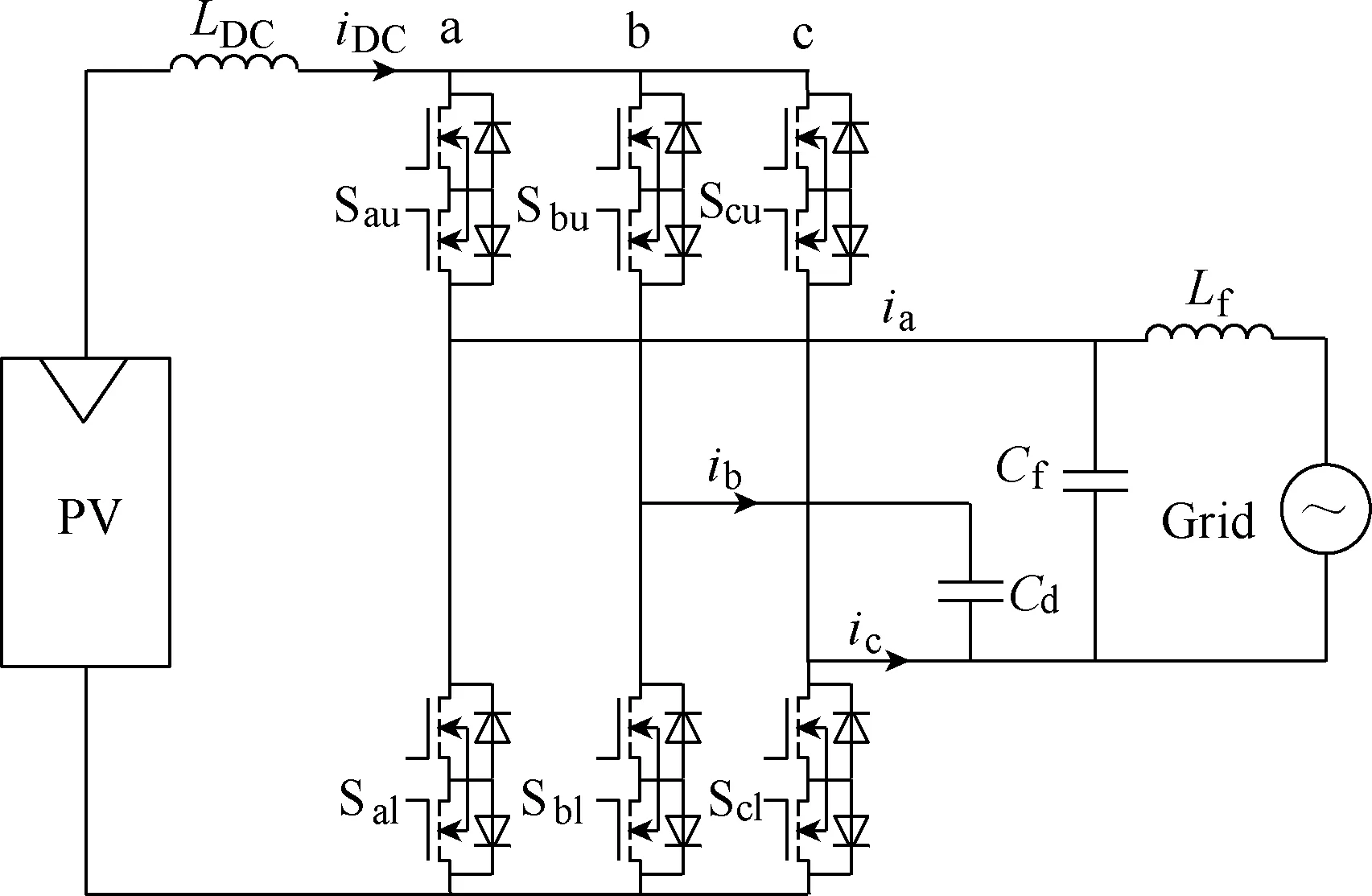
Fig.10 Topology proposed by Bush, et al[22]
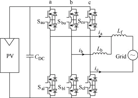
Fig.11 Topology proposed by Chen, et al[23]
Zare[25]proposed a three-port micro-inverter as shown in Fig.12. It is a modified single-phase flyback inverter that is derived from the conventional flyback inverter by incorporating an auxiliary winding in transformer and a power decoupling circuit. The decoupling circuit implements power transmission with the other two ports by interfacing the auxiliary winding.In this design, power switch in decoupling circuit is eliminated and the main switch S1operates in zerovoltage-switching condition, which increases overall design difficulty. Fortunately, system loss is reduced remarkably because of soft-switching technique and fewer components are used. Another typical three-port converter is illustrated in Fig.13.
A micro-inverter with AC-DC decoupling topology was proposed by Wang, et al[29], as shown in Fig.14,where the modular links AC and DC port with shorter power flowing path. In this design, power loss is reduced for power pulsation only flows through decoupling circuit while that flows through more power stage in other decoupling methods. This circuit operates as current source by controlling midpoint voltage between two series capacitors. Voltage ofCd1follows the command while voltage ofCd2reverses because the total voltage of series capacitors is confined by grid voltage.With this implementation, the power pulsation can be decoupled by series film capacitors of decoupling circuit.
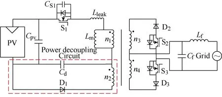
Fig.12 A three-port micro-inverter proposed by Zare, et al[25]
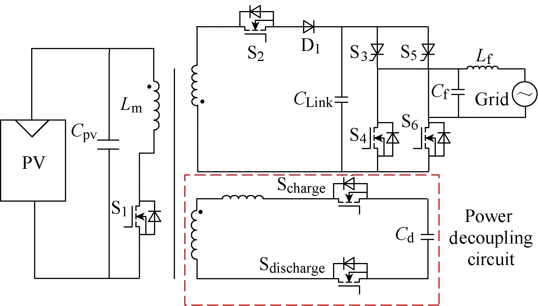
Fig.13 A typical three-port micro-inverter proposed by Kim, et al[26]
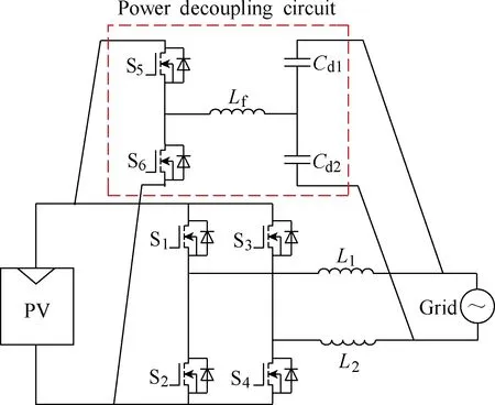
Fig.14 AC-DC decoupling topology proposed by Wang, et al[29]
4 Comparison of power decoupling methods
The aforementioned decoupling methods are classified and summarized in Tab regarding efficiency,component number, technical features, and so on.
PV side decoupling techniques depend on power decoupling circuits that consist of extra components,which influence system efficiency. Peak current control is commonly employed in this type of methods because of flyback converter used in PV side decoupling topology. A three-port micro-inverter decouples power pulsation by connecting decoupling circuit to an auxiliary winding in transformer. Considering reduced cost of the decoupling circuit, a three-port topology may be a good choice for a inverter with one port implementing MPPT and a second port dedicated to power decoupling[4]. Control complexities of three-port decoupling topologies and PV side decoupling topologies are similar. As for DC-link decoupling methods, they are only used in multi-stage topologies. System efficiency and cost are improved as a result of eliminating the power decoupling circuit. Meanwhile, by employing special control algorithms, voltage ripple across DC-link are high enough to reduce decoupling capacitance effectively without affecting current injected grid.However, high voltage ripple across DC-link increases switch stress and deteriorates system stability significantly. AC side decoupling technique seems to be an alternative scheme for multi-stage micro-inverters.Considering high voltage swinging in AC side,decoupling capacitance may be also reduced to a small value. Unfortunately, research on AC side decoupling is insufficient.
5 Feasibility analysis on a potential technological route
Given the above, existing decoupling methods of DC-link and AC side suffer from such problems as poor reliability and complex control. A potential technology route is proposed by the author to solve these problems.As show in Fig.15, a decoupling circuit is in parallel with AC side but not embedded in the inverter as phase leg. The decoupling circuit is independent of the power stage, improving reliability and cost using high voltage in AC side to reduce capacitor size.
Between the PV panel andCDCis the first stage, a boost converter with MPPT capability. The second stage is an H-bridge inverter that injects required current to grid. Constant power,PI, flows through the H-bridge inverter because power pulsation is handled by decoupling circuit, and power balance is realized.Consequently, no large capacitor is needed to smooth significant voltage ripple across DC-link.
The scheme has advantages as shown below:
(1) Thanks to high voltage swinging in AC side, the size of decoupling capacitor can be reduced to smaller than that in PV side decoupling.
(2) No special algorithms in DC-link decoupling methods are required and reliability is improved.
(3) Bidirectional switches used in present AC side decoupling methods are cancelled and control complexity is reduced.

Fig.15 A micro-inverter with power decoupling circuit across AC side
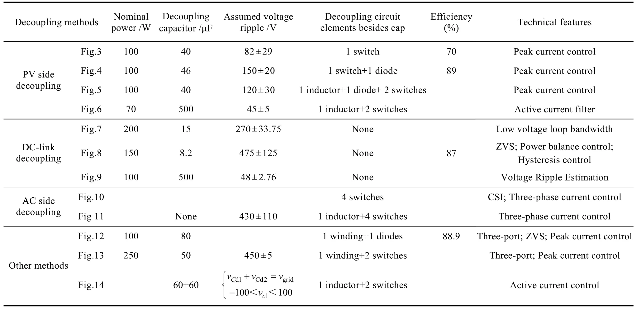
Table Comparison of different power decoupling methods
6 Conclusion
This paper reviews various power decoupling methods. A great deal of research has been conducted to reduce decoupling capacitance and increase the lifespan of micro-inverters. Efficiency of PV side decoupling method is limited by the decoupling circuit. Three-port decoupling method is a viable approach to reduce the cost of power decoupling circuit. For multi-stage micro-inverters, DC-link decoupling is the most mature scheme. Many sophisticated control strategies are employed to amplify high voltage ripple across DC-link capacitor. Thus, DC-link capacitance can be reduced effectively, although system reliability is affected. As for AC side decoupling, an additional leg is incorporated with an inverter stage to implement power decoupling.Decoupling capacitance is reduced at the cost of complexity and cost. Last but not least, a potential technological route for AC side decoupling is proposed for further study. A laboratory prototype is being constructed and the detail experimental results will be reported in the future publications.
 Chinese Journal of Electrical Engineering2018年4期
- Chinese Journal of Electrical Engineering的其它文章
- Battery Charging Method for Electric Vehicles:From Wired to On-Road Wireless Charging
- Using Inverter-Based Renewable Generators to Improve the Grid Power Quality—A Review
- Resonance Active Damping and PCC Voltage Quality Improvement of DFIG System Connected to Parallel Compensated Grid
- The Characteristics Analysis and Cogging Torque Optimization of a Surface-Interior Permanent Magnet Synchronous Motor
- Field-Oriented Control and Direct Torque Control for a Five-Phase Fault-Tolerant Flux-Switching Permanent-Magnet Motor
- Study of Pressure Balance for Press-Pack IGBTs and Its Influence on Temperature Distribution
