Study of Pressure Balance for Press-Pack IGBTs and Its Influence on Temperature Distribution
Zihao Zhao,2, Lin Liang*, and Lubin Han
(1. State Key Laboratory of Advanced Electromagnetic Engineering and Technology, School of Electrical and Electronic Engineering, Huazhong University of Science and Technology, Wuhan 430074, China;2. School of Optical and Electronic Information, Huazhong University of Science and Technology, Wuhan 430074, China)
Abstract: Pressure balance is a key technology for Press-Pack IGBT packaging, and is studied in this paper with its influence on the temperature distribution discussed in further when the device is turned on. By establishing the physical model of the Press-Pack IGBT device in the finite element simulation software, the influence of the internal flatness condition on the pressure balance is analyzed,and the variation of the average pressure difference with the flatness in different parallel scale of the chips is obtained. The thermal contact resistance and the electrical contact resistance parameters,which are dependent on the pressure, are then imported to perform the multi-field coupling, further investigating the effect of different pressure distributions on temperature distribution. The junction-case thermal resistance of the device with different flatness is compared experimentally. The results have demonstrated the influence of the flatness on the thermal resistance of the Press-Pack IGBT device.
Keywords: Press-Pack IGBT, pressure balance, temperature distribution, thermal resistance.
1 Introduction
The packaging design concept of high-power Press-Pack IGBT(Insulated Gate Bipolar Transistor) is derived from the common Thyristor and IGCT (Integrated Gate Commutated Thyristor). As a new high-power semiconductor device, the soldering and wire bonding are eliminated in Press-Pack IGBT, with the components such as electrodes and chips connected only by pressure.
As far as research status is concerned, the Press-Pack IGBT doesn't have a long history. ABB[1]in Switzerland,IXYS UK Westcode Ltd[2]in UK and Toshiba[3]in Japan have owned the key technology. In China, Zhuzhou CRRC Times Electric Co. Ltd[1]is representative and has done some research.
As a new form of packaging, research on Press-Pack IGBT devices is generally performed by finite element simulation methods , establishing thermal, electrical, and mechanical models[4-7]. T. Poller et al[8-10]successively studied the temperature distribution of IGBT chip and the influence of pressure distribution during power cycling through finite element method in 2012, and studied the influence of external pressure on current,pressure and temperature distribution of IGBT chip inside the device in 2013. Further, the relationship between the clamping pressure, electrical contact resistance and thermal contact resistance of the chip was obtained through experimental measurements. A.Hasmasan et al[11]. studied the impact of different installation conditions on the internal pressure and temperature distribution of the device through the finite element method and the IGBT chip thermal network model in 2013. Deng Erping[12-13]conducted numerical calculation and experimental verification on the thermal contact resistance between single FRD sub-module components in the Press-Pack IGBT device in 2016, thus to study the effect of temperature on contact thermal resistance. The influence of machining deviation and internal layout on the pressure distribution of each component was also studied, by design of the sub-module layout. For the Press-Pack IGBT device, the processing accuracy of each sub-module directly affects the performance of the device. The differences in height of sub-modules causes uneven pressure distribution,which leads to the difference of electrical contact resistance and thermal contact resistance, and ultimately affects the temperature distribution of the chips. The impact also varies with the scale of the chips in parallel.There is still lack of clear statement for the issue.
The research in this paper is for the Press-Pack type.The structural model is established in the finite element simulation software and imported into the mechanicalelectrical-thermal field to realize multi-field coupling.The impact of internal flatness of the device on temperature distribution of the chips is studied. The junction-case thermal resistance of three devices with different flatness was designed and measured, so as to verify the effect of flatness on the junction-case thermal resistance and the junction temperature of the chips.
2 Finite element model
2.1 Packaging structure
There is a collector molybdenum plate, an IGBT chip, an emitter molybdenum plate a silver plate and a locating frame in top-down arrangement in a Press-Pack IGBT sub-module. The gate of the IGBT chip and the PCB for interconnection are connected by a gate spring,thus the gate current is derived through the external gate lead. These components are fixed by the locating frame,each component is placed into the frame by mechanical alignment, and the entire sub-module is placed on the emitter pedestal. After all the sub-modules are installed,they are packaged in a ceramic case, and the inside is evacuated and filled with inert gas. The case is in the form of the insulator structure, which mainly serves as insulation and protection. A structural view of the Press-Pack IGBT sub-module is shown in Fig.1.
2.2 Simulation conditions
The models of 9, 16 and 25 IGBT chips in parallel are respectively established, and the sub-modules are arranged in a square manner, so as to ensure the structural symmetry. In the model, the heat sinks are installed on both sides of the emitter and collector of the device[14-16]in order to be consistent with practical applications.
The external clamping pressure should be determined by the total area of the chips, so as to ensure the electrical and mechanical properties of the Press-Pack IGBT device, reducing the thermal contact resistance and the electrical contact resistance between the components to a relatively low value. The stress should be around 12MPa[17]. The boundary conditions of the finite element simulation model are shown in Fig.2. The components (materials) from top to bottom are: heat sink on collector side (copper), collector (copper), collector molybdenum plate (molybdenum), IGBT chip (silicon),emitter molybdenum plate (molybdenum), pedestal(copper), emitter (copper) and heat sink on emitter side(copper). For the contact surface setting, the contact l between the heat sink and the two electrodes is set to be Bonded, while other contact surfaces are set to be Frictional and the frictional coefficient is set to be 0.5[18].On the outer surface of the heat sink on collector side is the uniformly distributed clamping pressure, which is obtained from 12MPa multiplied by the total area of the chips. On the outer surface of the heat sink on emitter side is fixed support.

Fig.1 Press-Pack IGBT sub-module structure diagram
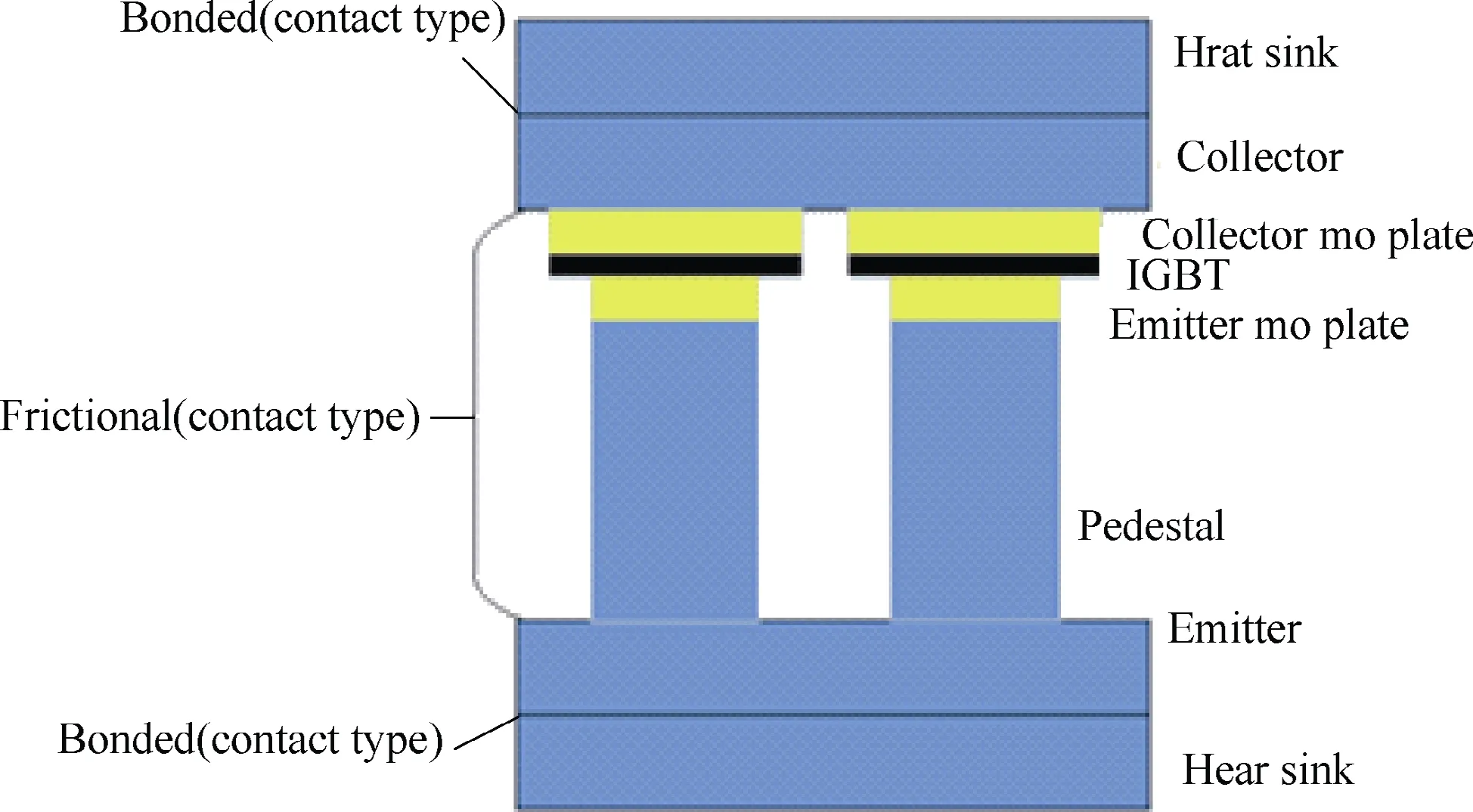
Fig.2 Boundary conditions of the Press-Pack IGBT mode
3 Analysis of pressure balance
The established model is imported into the mechanical field of the finite element simulation software, and the elastic parameters of the material are set[19,20]as shown in Table 1.
Firstly, the Press-Pack IGBT model is analyzed under the ideal condition, with the same height of each sub-module. The emitter-side stress distribution on the chips contacted with the molybdenum plates in 25-chip parallel model is shown in Fig.3. It can be seen that the stress on the chips is evenly distributed, but the stress on the middle chips is smaller than that of the outer ones.This is because the copper electrode is deformed under the impact of pressure, and the chips on the outer side are subjected to additional stress.
In order to analyze the effects of machining error and assembly error, the height of a sub-module located on the outer side is reduced by 1μm each time by the assumption made in this paper, until there is no stress change on the chips. The average stress on each chip is extracted to study the stress distribution of the chips for different flatness. The stress distribution on the chips is shown in Fig.4, when the height of a single sub-module is reduced by 1μm and 9μm in 25-chip parallel model.As can be seen, when the height of a single sub-module is reduced by 1μm, the stress on the chip in the sub-module is drastically reduced, and the stress on the adjacent chip is sharply increased, resulting in uneven stress distribution on the chips. When the height of a single sub-module is reduced by 9μm, it can be seen that there is almost no stress on the chip in this sub-module,while stress concentration still occurs on the chip next to it. In practical applications, not only are the electrical characteristics and mechanical characteristics of the sub-modules with reduced height not guaranteed, but also other sub-modules are also affected.

Table1 Elastic parameters of materials

Fig.3 Emitter-side stress distribution on chips in 25-chip parallel model under ideal conditions
In order to make some comparisons, the stress on the surface of the chips when the height of the single sub-module is reduced by from 1 to 11μm is recorded, in which 9, 16 and 25 IGBT chips are in parallel, separately.The result is shown in Fig.5.dis the reduced height of the single sub-module, and ΔPis the difference between the average stress on the chip in the sub-module with a reduced height and the average stress on other chips. As can be seen from Fig.5, in general, the larger the chip parallel scale is, the greater the influence of the flatness difference on the pressure balance of the Press-Pack IGBT is. The greater the flatness difference is, the more severe the uneven pressure distribution is. There is an anomaly point. Whendis from 1 to 2μm, the ΔPof the 25-chip parallel model is smaller than the ΔPof 9 chips and 16 chips, which may be due to the larger copper electrode area of the 25-chip parallel model. During the clamping process, when the deformation of the copper electrode occurs, the extra stress on the chips on the outer side of the 25-chip parallel model is greater than that of the 9 chips and the 16 chips. Whendreaches 9μm and above, ΔPdoes not change any more, and it can be considered that the sub-module is no longer in contact with the copper electrode.
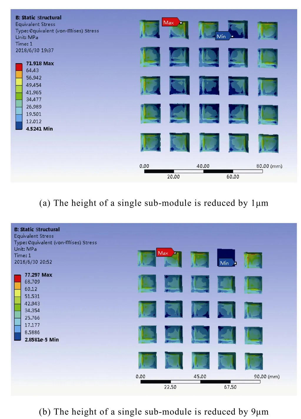
Fig.4 Emitter-side stress distribution on the chips in the 25-chip parallel model

Fig.5 Relationship between ΔP and d in 9,16 and 25 chip parallel models
4 Analysis of temperature balance
4.1 Mechanical-electric-thermal field coupling
In order to study the influence of the flatness on the temperature distribution of the Press-Pack IGBT chip,the mechanical model is imported into the electricalthermal field to perform the multi-field coupling simulation. The contact pressure affects the thermal contact resistanceRthand the electrical contact resistanceRel, and the calculation formulas are as shown in (1) and(2).ECC(Electrical Contact Conductance) andTCC(Thermal Contact Conductance) are determined according to the stress on the chip recorded under different flatness mentioned above. T. poller et al. obtained the experimental and computational analysis of theECCandTCCwith the variation of contact pressure in the range of 750~2500N when the surface contact is between aluminum and molybdenum[10]. For the accuracy of the results, theECCandTCCvalues corresponding to the pressure on the chips are taken only when the height of the sub-module is reduced by 1~5μm in 25-chip parallel model. The pressure range is 900~2100N. The relationship between the contact pressureFto which chips are subjected and theTCCorECCis shown in Fig.6.

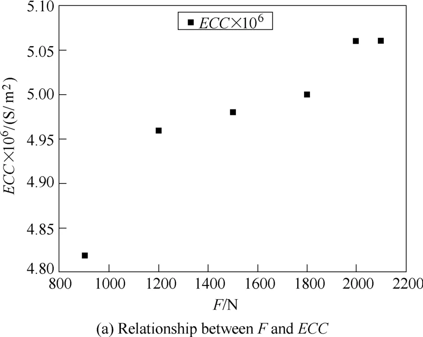

Fig.6 Relationship between ECC, TCC and F in the 25-chip parallel model
4.2 Simulation results and analysis
The thermal-electrical field simulations of the chip parallel model are carried out, and then the temperature distributions of the chips are obtained when the height of the single sub-module is reduced by 5μm in 25-chip Press-Pack IGBT model, as shown in Fig.7. It can be seen that the temperature of the chip in the sub-module with reduced height is significantly higher than those of other chips. As the contact pressure decreases, the electrical contact resistance and the thermal contact resistance increase simultaneously. When the IGBT device is turned on, the increase in electrical contact resistance causes a decrease in ohmic dissipation, thus the increase in temperature is suppressed. The increase in contact thermal resistance causes poor heat dissipation,thus the rise in temperature is accelerated. But the thermal contact resistance has much greater impact on the chip temperature than the electrical contact resistance does.
The temperature distribution of the chips in the 25-chip parallel model, in which the height of a single sub-module is reduced by 1~5μm, is shown in Fig.8. ΔTjis the difference between the junction temperature of the chip in the sub-module with a reduced height and the average junction temperature of other chips. In order to further compare the effects ofECCandTCCon the chip temperature, firstly theECCandTCCare set separately and then set together in the contact conditions.
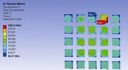
Fig.7 Temperature distribution of the chips when the height of a single sub-module is reduced by 5μm in the 25-chip parallel model

Fig.8 Relationship between ΔTj and d in the 25-chip parallel model
As can be seen from Fig.8, as the flatness deteriorates, the temperature balance between the chips also deteriorates correspondingly. The increase ofTCCandECChas the opposite impact on the temperature of the chips when the pressure is reduced, while the impact ofTCCon temperature of the chips is much greater than that ofECC. Therefore, in the packaging process, if the clamping pressure on the chip is too small, the junction temperature of the chip may be too high, which may adversely affect the normal operation of the device.
5 Experimental verification
5.1 Experimental principle and platform construction
In order to verify the analysis, a 24-chip Press-Pack IGBT device, with the ratio of the IGBT and FRD chips is 1:1, is designed and packaged. The device clamping platform is shown in the Fig.9.
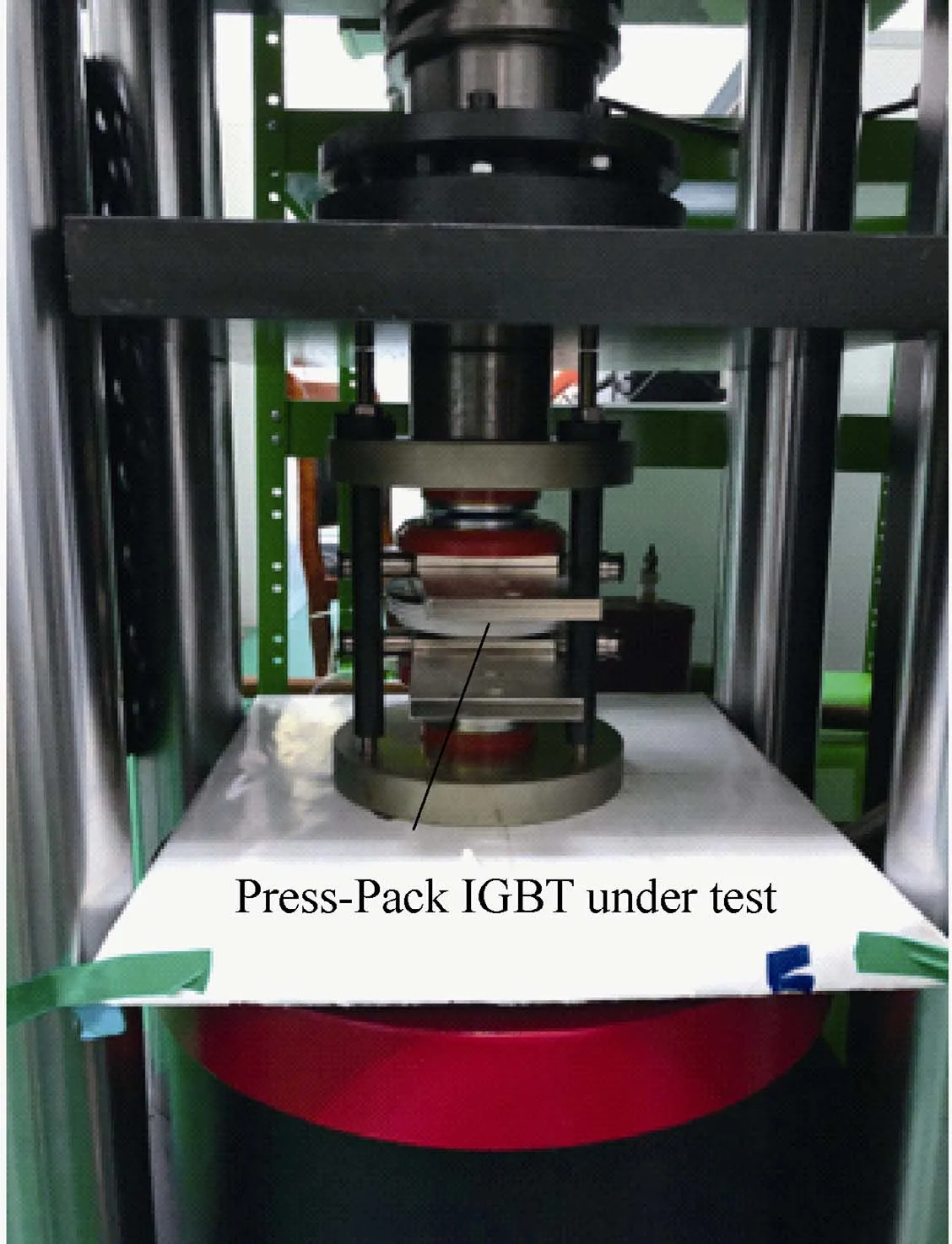
Fig.9 The clamping platform for the device
Experiments were carried out by using cases with different internal flatness. The junction-case thermal resistance of different cases is measured and calculated,and the relationship between the flatness and temperature balance of the Press-Pack IGBT devices is verified by comparison of the data. The position distribution diagram of the four-sub-module is shown in Fig.10. Four IGBT sub-modules are taken counterclockwise, with the gate pin as a reference, and are respectively labeled as 1, 2, 3,and 4 in order. The four sub-modules are assembled.
The thickness of each component of the sub-module is measured by a Mitutoyo comparator, and the results are shown in Table 2.
Three different cases are labeled as case I, II, and III. The heights of the emitter pedestal of the four sub-modules are measured. The results are shown in Table 3. It can be seen that the flatness is getting better from case I to case III.
In order to maintain the difference in flatness during the experiment, the components of the submodules are arranged by the thickness, and are assembled in order of the height of the sub-modules. The IGBTs are packaged with the cases I, II, and III with the same components of the four sub-modules. Three sets of junction-case thermal resistance are measured for comparison.
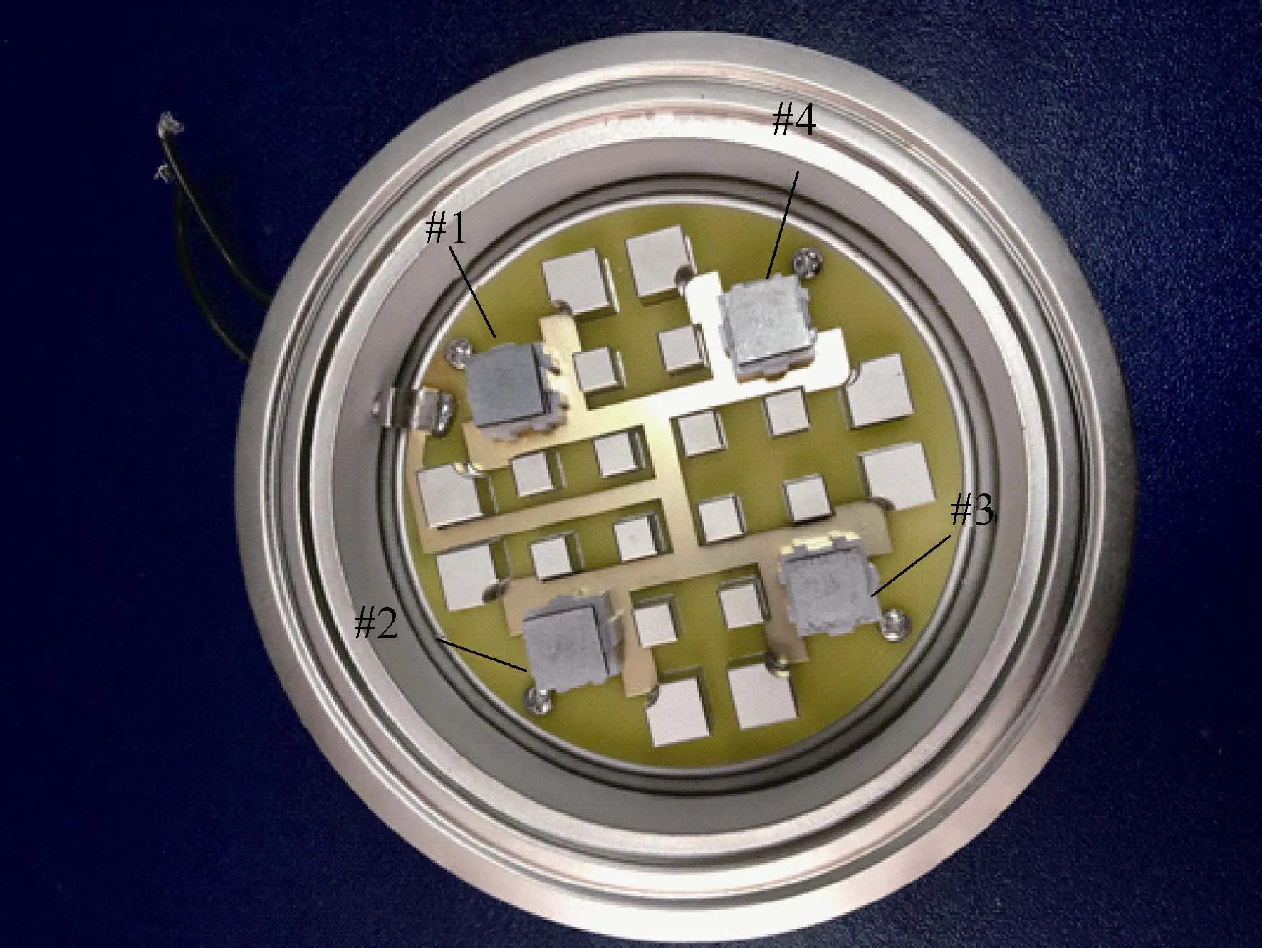
Fig.10 The position distribution of the four sub-modules

Table 2 Thickness of each component of the sub-module(unit: mm)

Table 3 Height of the emitter pedestal of the four sub-modules from case I to III (unit: mm)
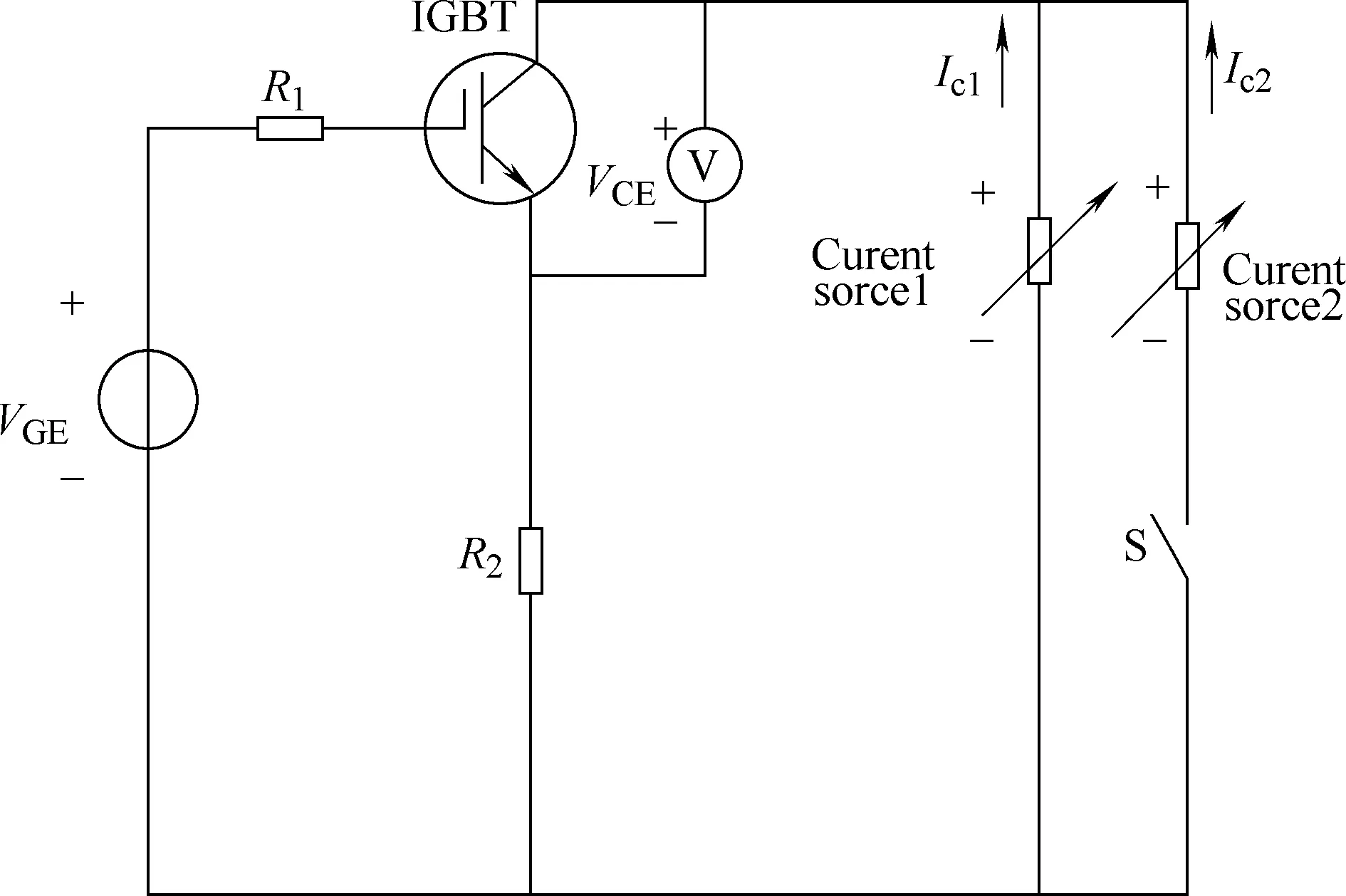
Fig.11 The schematic diagram of the thermal resistance measurement
The schematic diagram of the thermal resistance measurement is shown in Fig.11.Ic1is a low current that just makes the IGBT saturated, andIc2is a high current below the IGBT's current rate. First, the coefficientKof the collector-emitter voltageVCEversus the junction temperatureTjof the chip is measured, and the relationship is fitted. Then the switch S is turned on to reach the thermal equilibrium of the device and the case temperatureTcis measured. After that, the switch S is turned off. TheVCEis measured immediately at the moment of the turn-off. The value of theVCEis plugged into the fitted relationship, and the corresponding junction temperatureTjis obtained. The average powerPof the high current source in the steady state is calculated according toVCEandIc2. The junction-case thermal resistanceRth(j-c)is calculated[21]by equation (3).The experimental platform built according to the circuit diagram[22]is shown in Fig.12.

5.2 Analysis of the results
The junction temperature coefficient of theVCEof the IGBT chip is negative. The device is heated to measure the value ofVCEat different temperatures. The fitted relationship is shown in Fig.13, and the fitted equation is shown as (4).


Fig.12 The experimental platform for the thermal resistance measurement

Fig.13 Fitted relationship of VCE-Tj of the device packaged with case I
VCEis measured with an oscilloscope, and the time nodes before and after the shutdown are taken. The variation ofVCEwith time is shown in Fig.14. The value ofVCEat the lowest point of the image after the shutdown is taken, which is seen as the IGBT collector voltage value at the moment of turn-off. Then the value is substituted into (4) to calculate the junction-case thermal resistanceRth(j-c).TheRth(j-c)of the device packaged with case I is 0.393K/W.
The junction-case thermal resistanceRth(j-c)of the device packaged with case I, II, and III is calculated, as shown in Table 4.
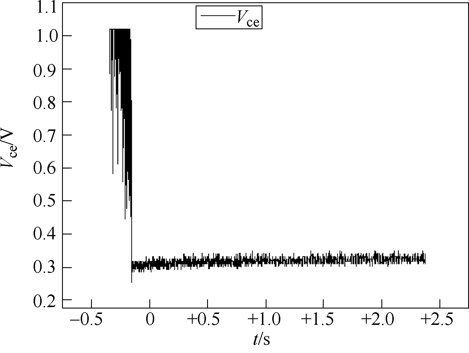
Fig.14 The variation of VCE with time t for device packaged with case I
As can be seen from Table 4, when case Ⅰis compared with case Ⅲ, the temperature difference of the junction-case is increased by 7.59% and the junction-case thermal resistance is increased by 67.2%.In the case of the same high current excitation, the better the flatness of the case is, the lower the junction temperature is. The analysis of this paper is verified: the better the flatness is, the more uniform the pressure distribution of the chips is, the smaller the thermal contact resistance of the device (the entire thermal resistance of the device) is, and the lower the junction temperature of the chips is.
6 Conclusion
The multi-field coupling model of the Press-Packed IGBT device is established to study the influence factors of pressure balance and its influence on the temperature distribution in this paper. The pressure distribution of the chips under different flatness, together with the temperature distribution of the chips under different pressure distribution is analyzed. After experimental verification, the following conclusions were obtained:
(1) By establishing the mechanical model of the Press-Packed IGBT, the stress of the chips under different flatness is simulated and analyzed. The worse the flatness is, the worse the pressure balance of the device is. This case becomes more serious when the scale of the parallel chips becomes larger.
(2) By establishing the IGBT mechanical-electricthermal multi-field coupling model, the temperature distribution of the chips for the on-state of the device is simulated and analyzed under different flatness. When the stress of the chips changes, the thermal contact resistance and the electrical contact resistance between the chips and the molybdenum plates are also change.The influence of the electrical contact resistance on the junction temperature of the chip is much smaller than that of the thermal contact resistance. As the flatness deteriorates, the thermal contact resistance rises and the heat dissipation deteriorates, then the temperature balance between the chipsets also deteriorates accordingly.
(3) The IGBT chips are packaged with three cases under different internal flatness, and the junction-case thermal resistance of the three devices is measured. It is shown in the results that the worse the internal flatness of the device is, the larger junction-case thermal resistance is, and the higher the junction temperature of the chips is.
 Chinese Journal of Electrical Engineering2018年4期
- Chinese Journal of Electrical Engineering的其它文章
- Research on Clustering Equivalent Modeling of Large-Scale Photovoltaic Power Plants
- No-Load Iron Loss Model for a Fractional-Slot Surface-Mounted Permanent Magnet Motor Based on Magnetic Field Analytical Calculation
- Microgrid Relay Protection Scheme Based on Harmonic Footprint of Short-Circuit Fault
- Field-Oriented Control and Direct Torque Control for a Five-Phase Fault-Tolerant Flux-Switching Permanent-Magnet Motor
- The Characteristics Analysis and Cogging Torque Optimization of a Surface-Interior Permanent Magnet Synchronous Motor
- Resonance Active Damping and PCC Voltage Quality Improvement of DFIG System Connected to Parallel Compensated Grid
