Circuit Implementation of Power Converter for High-Speed Switching Operations
(Department of Electronics Engineering and Computer Science, Tokyo Metropolitan University, Tokyo Japan)
Abstract: Recently, high di/dt and dv/dt switching operations of power converter circuits has been discussed for realizing a high-efficiency power converter circuit. In this case, parasitic inductances of the bus bar between a DC capacitor and power devices may cause issues of overshoot voltage and electromagnetic interference(EMI) noise. Therefore, it is necessary to design the bus bar geometry while considering the minimization and optimization of the parasitic inductance of bus bar. This paper discusses a relationship between bus bar geometry and switching characteristics. In addition, the bus bar analysis is based on the PEEC method, and the bus bar geometry is designed by considering the stray inductance with using an inductance-map method. Moreover, this paper also presents a design procedure of acceptable stray inductance based on a standardization method. It should be noted that the stray inductance is designed not for minimization, but optimization, and it is shown not as an absolute value(H), but as a percentage value(%). Finally, the oscillation waveforms under turn-off operation will be discussed depending on the bus bar geometry.
Keywords: Bus bar inductance, bus bar geometry, circuit implementation, EMI, switching characteristics.
1 Introduction
In recent years, a power semiconductor device capable of high-speed and high-frequency switching has been developed[1-5], and further higher power density of the power converter circuit has become possible.However, the influence on the parasitic inductance of the DC side wiring between DC capacitor and power devices may occur, and many papers have reviewed this through simulation and experimentally[6-11]. By reducing the parasitic inductance, it is possible to suppress the overshoot voltage during the turn-off operation. However, both the switching loss and electromagneticon noise largely differs depending on driving conditions of power semiconductor. In other words, it is required not only to reduce the parasitic inductance but also to design the inductance to an optimum value[11-13]depending on circuit conditions.The parasitic inductance of the DC side wiring is determined by the wiring geometry connecting the DC capacitor and the semiconductor device.
In recent years, a bus bar geometry capable of low parasitic inductance and large current capacity has been adopted in the power conversion circuit. It has been reported that the laminated bus bar geometry[14-16]in which the bus bars are arranged close to each other in parallel is effective for minimizing the parasitic inductance. For parasitic inductance analysis, generalpurpose electromagnetic field analysis software[17-18]using finite element method is applied. It is very useful for analysis of the complicated wiring structure and influence of the current distribution inside the bus bar. In addition, it may take a long time to execute model creation and analysis. On the other hand, partial element equivalent circuit(PEEC) method has been proposed,and it is possible to perform highly accurate calculation by dividing the bus bar[19-21]. Frequency characteristics of bus bar inductance considering the skin effect are also presented, and it is shown that inductance fluctuation of DC to 1MHz or less is within 3%. However, the conventional method has constraints on calculation conditions, and there are cases where the number of divisions becomes unmanageable to maintain calculation accuracy.
This paper presents a procedure of circuit implementation for power converter circuit implementation.Firstly, an inductance map can clarify the relationship between the wiring geometry and the inductance value.Furthermore, it is verified that wiring structure design that satisfies arbitrary inductance value is possible by using this map. In addition, this paper presents a design procedure of acceptable stray inductance based on a standardization method. It should be noted that the stray inductance is designed not for minimization, but optimization, and it is shown not as an absolute value(H),but as a percentage value(%). By applying the proposed method, a maximum stray inductance can be designed for power electronics circuits, considering the voltage and the current ratings of semiconductor devices. In order to verify the proposed method, the experimental results are demonstrated using a SiC-MOSFET with voltage and current ratings of 500V and 400A,respectively. Finally, the oscillation waveforms under turn-off operation will be discussed depending on the bus bar geometry.
2 Parasitic inductance within power converter circuit
2.1 Parasitic inductance
SiC and GaN power devices are capable of faster switching operations compared with Si devices, although they present significant issues attributed to “surge voltage” and “oscillations” generated during turn-off operations. It is especially required not only for power device destruction caused by surge voltage but also because of the increased switching loss. Fig.1 shows an ideal buck converter circuit, which is the basis of a power converter circuit. Fig.2 shows a circuit diagram including the parasitic inductance of wiring attributed to an actual wiring structure. Here, a capacitor between the DC power supply and the power device, the internal parasitic inductance of the gate drive circuit, and MOSFET source-side inductance are illustrated. The voltagevdsappearing on both ends of the MOSFET generated when the MOSFET is turned off is given by the following equation.

Here,Lsrepresents the sum total of the parasitic inductance of an inverter circuit, which is the main cause of surge voltage. Reducing the inductance is an effective method of reducing the surge voltage generated at switching. The parasitic inductanceLsis the total value,which is broadly divided into three values defined below.On the other hand, the inductanceLshould be considered an analysis of the detail circuit operation.
(1) Internal inductance dependent on the internal structure of a capacitorCused on the DC side.
(2) Internal inductance of the power module—mainly parasitic inductance between the semiconductor chip and terminal.
(3) Parasitic inductance of the wiring connecting the above capacitor and power device.
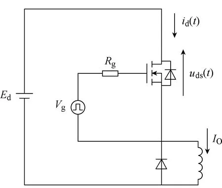
Fig.1 Buck converter circuit
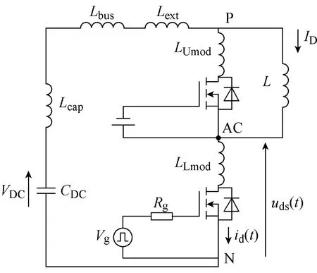
Fig.2 Buck chopper circuit including parasitic parameters
The internal inductances of power modules and electrolytic capacitors have been included in data sheets.These inductances are determined by each component and thus cannot be set at the discretion of the electricalcircuit designer. Furthermore, the parasitic inductance of wiring is determined by the circuit geometry(thickness,length, cross-sectional area, conductor position), and thus cannot be set by wire or printed circuit board manufacturers. In addition, circuit designers generally do not actively set the parasitic inductance; this is largely dependent on the experience of circuit designer.Therefore, when designing circuits using SiC or GaN power devices, it must be recognized that circuits must be designed as critical electrical components determining surge voltage, not just as copper wire with zero parasitic inductance.
2.2 Design for parasitic inductance
The wiring of power converter circuit is used to connect electrical parts, and with consideration of the operations within power converter circuits. Therefore the parasitic inductance cannot be ignored. Generally,electrical and electronic parts are arranged in consideration of the physical structure, followed by the design of the wiring structure. Accordingly, conventional designs did not actively deal with parasitic inductance.However, in the case of recent power converter circuits with high-speed switching operations, the parasitic inductance must be set in advance to ensure safe circuit operation. Although the stray inductance is measured in Henrys(H), because power converter circuits have a variety of voltage and current ratings, circuit designers are unable to find common points of discussion through absolute values for inductance. For example, it is impossible to simply discuss whether a parasitic inductance of “1nH” is large or small for a circuit.
2.3 Upper and lower limits of parasitic inductance
Most papers discuss how to minimize a parasitic inductance so that the surge voltage generated at turn-off operations does not exceed the rated voltage of the power device. The parasitic inductance is attributed to wiring geometry connecting power devices and capacitors. Recently, laminate bus bars, which are wiring structures capable of reducing inductance, as shown in Fig.3, have been used. Hence, the dominant issue is the inductance affecting the interior of capacitors and the power-module internal inductance.
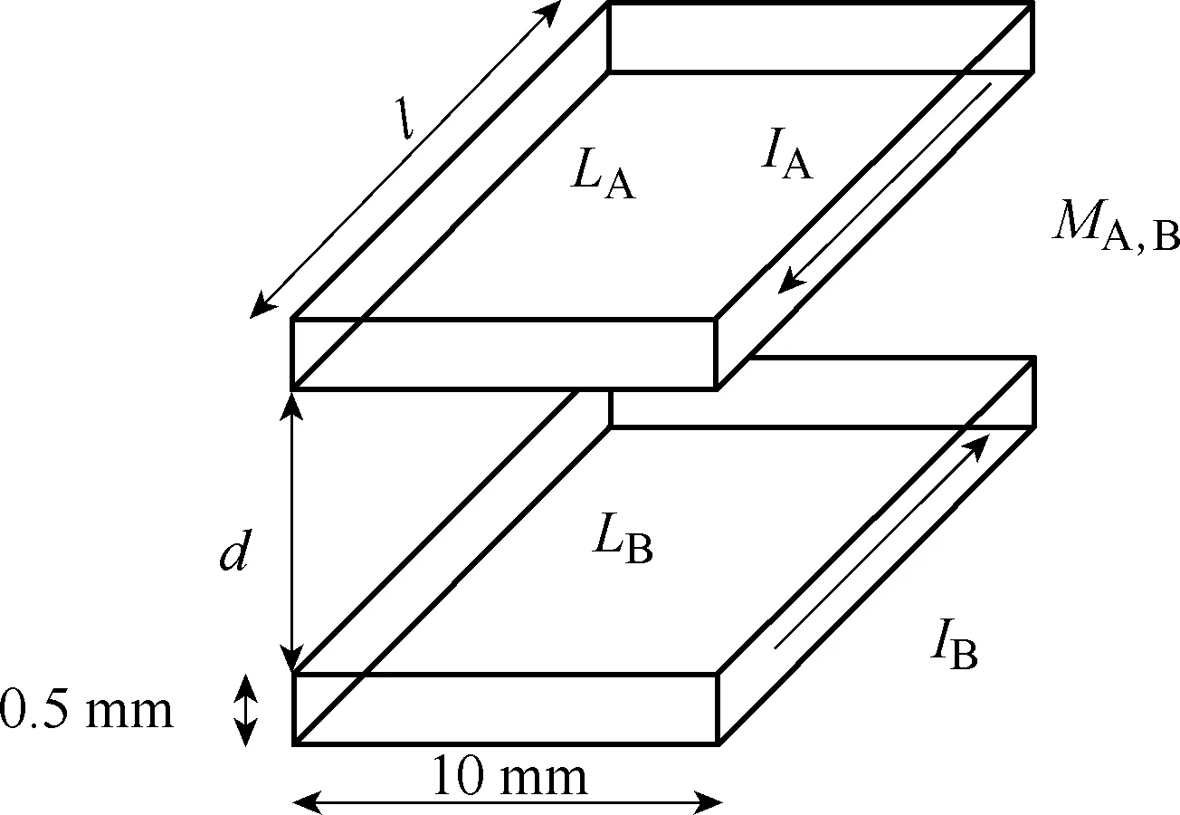
Fig.3 Laminated bus bar geometry
On the other hand, few studies discuss lower limit values for parasitic inductance. Lower limit values are related to the protection time for current-protection circuits. For example, in the case of short circuit operations, as the power devices upper- and lower-arm short circuits, the parasitic inductance plays a critical role in preventing a short-circuit current. Thus,inductance is extremely important regarding protection of power devices, and from the perspective of improving the circuit reliability, attention should not be paid not only to reducing it.
The parasitic inductance has both upper and lower limits, each changing according to the voltage current rating of the power device used. Therefore, a standardization of parasitic inductance with circuit impedance as a reference is discussed.
2.4 Techniques for analysing parasitic inductance
Reducing the wiring length is one technique for reducing the parasitic inductance. However, it is difficult to reduce the parasitic inductance, as it is closely related to the cross-sectional area of the wiring and the physical relationship between the conductors on a round-trip current pathway. There are two principles for analyzing the parasitic inductance.①Three-dimensional electromagnetic-field analysis;②Partial element equivalent circuit(PEEC) method.
Both methods are already available in commercial software. Its benefits and drawbacks are as follows:
Benefits:
· Capable of analyzing the inductance of real structures,making it applicable to complex structures.
· Capable of analyzing not only inductance, but also current distribution and other physical phenomena.
Drawbacks:
· Commercial software has multiple functions and comes in many types, but is quite expensive.
· Model creation and analysis time is extremely long.
· Results sometimes differ depending on the input value parameters.
3 Technique for setting parasitic inductance
3.1 Relationship between wiring structure and inductance
The relationship between the wiring structure and parasitic inductance is discussed. Here, a laminate structure as shown in Fig.3 and a parallel-plate structure in Fig.4 are shown, as two typical examples. The laminate structure has recently attracted attention owing to its low parasitic inductance.

Fig.4 Parallel-Plate bus bar geometry
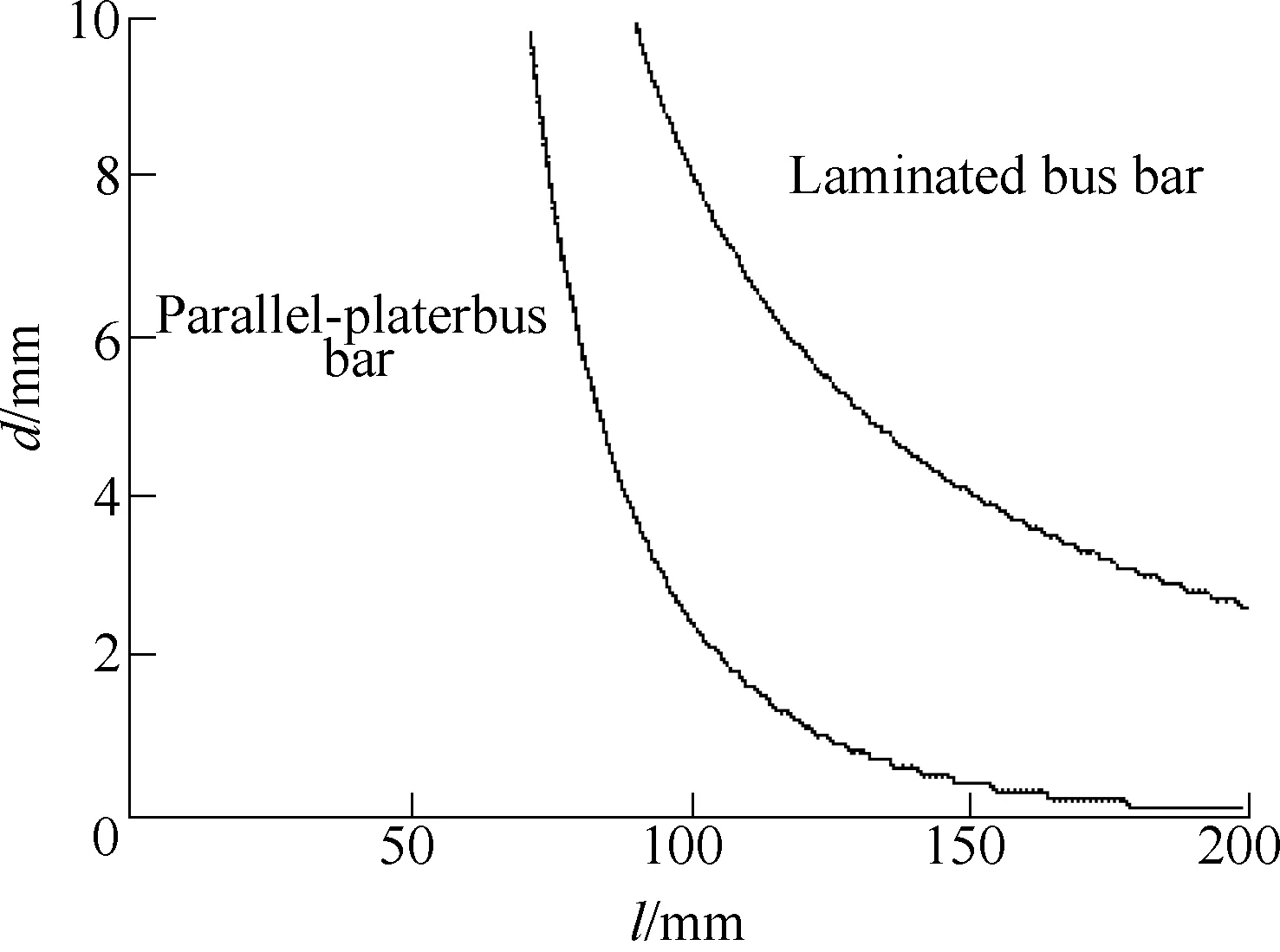
Fig.5 Inductance map for bus bar depending on the geometry
Fig.5 shows the analysis results of bus bar inductance, which is called “inductance map’’, depending on the geometry using the PEEC method to represent a wiring structure and an inductance structure with equivalent inductance lines. Assuming the cross-sectional area(t×w) of the wiring to be fixed, the distance between wires,d, and the line length, ℓ, are indicated by the vertical and horizontal axes, respectively, in Fig.5. The values correspond to a wiring structure reaching 50nH.Comparing these two figures reveals that the laminate structure offers greater design freedom for the wiring structure, as a wide range is required for a setting of 50nH or lower. For example, even if ℓ becomes large,adjusting the distance between wires changes the inductance value. These concepts are qualitatively well-known, but the Fig.5 is very useful for expressing them with specific numerical values.
The results of an analytical technique using the PEEC method do not account for effects such as the conductivity, skin effect, and current distribution.However, the technique is useful for power converter circuits currently in use. Additionally, even if the method is inadequate, it is considered that finding general forms using the relationship between the inductance and structure determined via the inductance map as an initial value and then using electromagneticfield analysis for detailed analysis makes it possible to greatly reduce the conventional number of trial and errors.
3.2 Standardization of parasitic inductance
The standardization of parasitic inductance using the surge voltage for reference is discussed. Fig.6 shows the equivalent-circuit diagram that is the subject of this discussion, and Fig.7 shows turn-off waveform at turn-off operations.
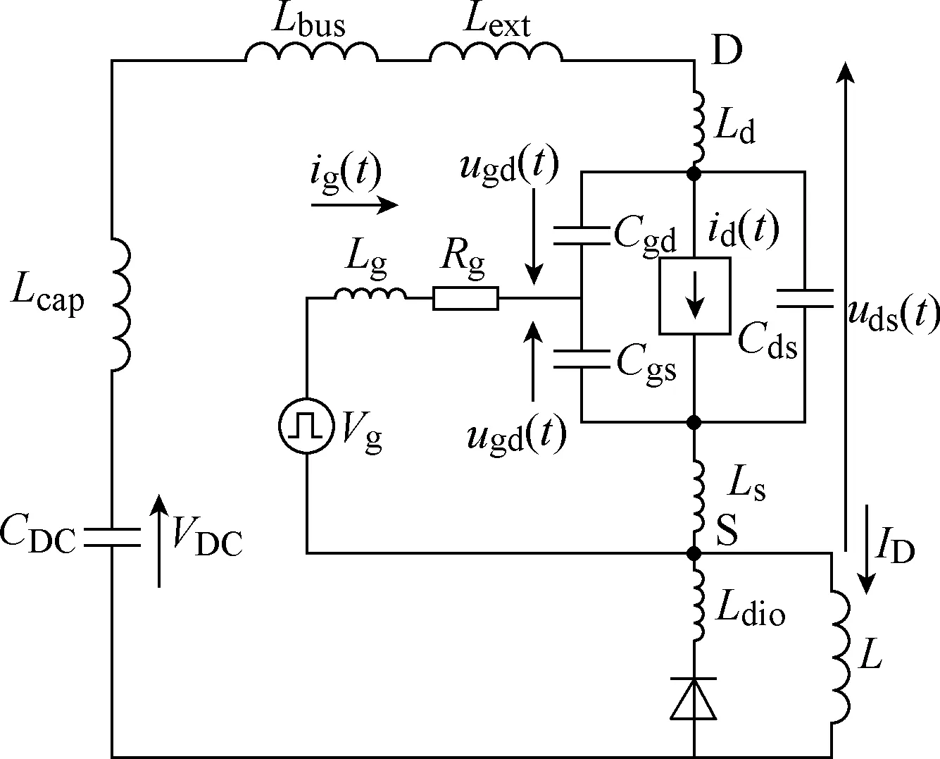
Fig.6 Circuit model for analyses the detail switching operation
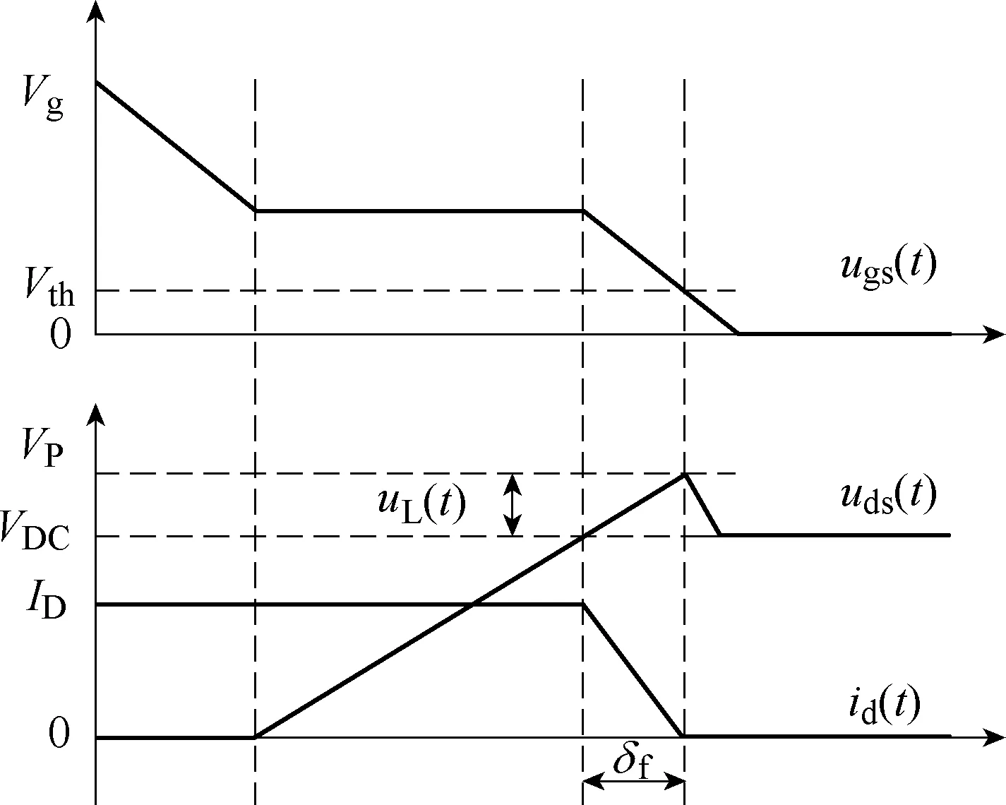
Fig.7 Switching operation of MOSFET
The ratioεof the DC power supply voltage to the surge voltage as follows.

The surge voltage is produced by the induced electromotive force due to the wiring inductance and corresponds to current changes at turn-off operation. The sum of this voltage and the DC voltage is produced at both ends of the power device and is expressed as follows.

In this case the parasitic inductance of the entire circuit is given as follows.

Here, the right second term in (3) isvL. When this is substituted into (2), the resulting modified formula is as follows.

Furthermore, as shown in Fig.7, the switching period current and time are approximated as follows.

From the above, the standardization impedance can be defined as follows.

This means that the impedance attributable to the parasitic inductance is expressed as a ratio.
This is modified as follows.

The standardization impedanceZ% and the value of the surge voltage become equal. That is, by determining the standardization impedance, it is possible to set the surge voltage. A benefit of this technique is that it is possible to uniformly set the parasitic inductance of the wiring even for power electronic circuits with different voltage current ratings.
3.3 Experimental verification of standardization impedance
This section presents a validation of the technique for setting parasitic inductance using the standardization impedance. As shown in the Fig.2, an experiment was conducted with a DC voltage of 500V.
Fig.8 shows the drain current and the voltage waveform between the drain and source when the drain-current of MOSFET current is set to 10A. The surge voltage occurs at 11%(556V) of the DC voltage. In addition, Fig.9 shows the waveform of each part when the drain-current is set to 60 A. In this case, the surge-voltage reaches 61%(806V). Thus, it can be confirmed that the surge voltage increases with the turn-off current, despite the condition that the circuit is equal.
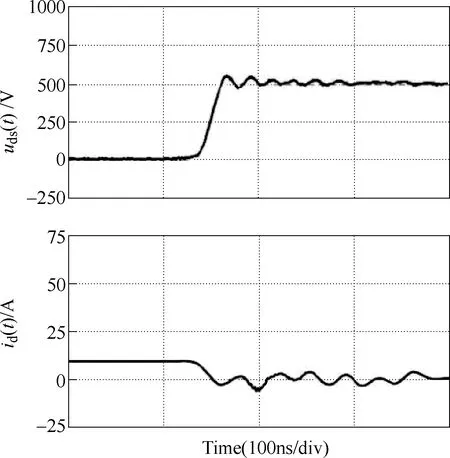
Fig.8 Experimental waveforms at 10A of the drain-current
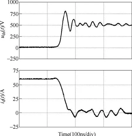
Fig.9 Experimental waveform at 10A of the drain-current
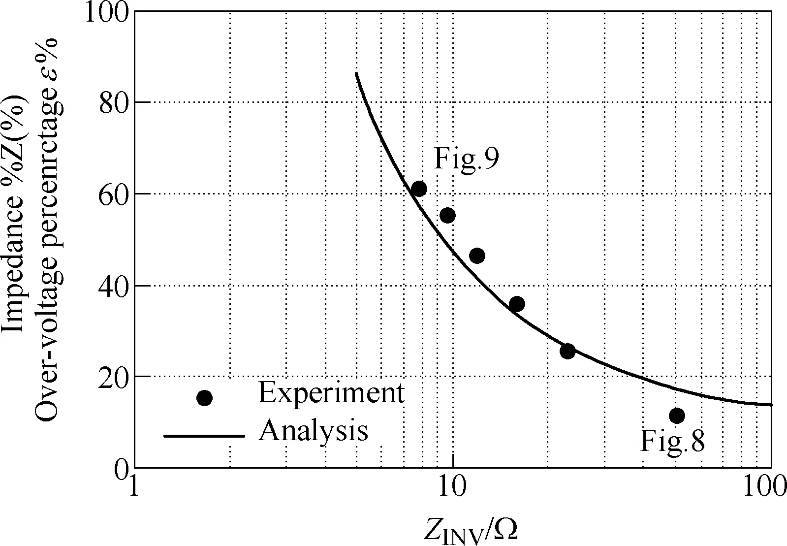
Fig.10 Relationship between the circuit impedance and over voltage
Fig.10 shows the results of the relationship between the circuit impedance and over-voltage percentage according to the standardization impedance. In this figure, the horizontal axis indicates the impedance, and the vertical axis indicates the surge voltage. The surge voltage increases when the standardization impedance is small. The solid lines indicate the analysis results, which closely match the experimental results. Because the required values for parasitic inductance differ depending on the circuit voltage and current rating, the parasitic inductance is not only discussed in terms of absolute values, but can be uniformly discussed using the standardization impedance, which is a percentage.
3.4 Technique for setting inductance using standardization impedance
The experimental circuit uses a SiC-MOSFET module rated at 500V, 430A buck chopper circuit. The switching period is determined using a power device data sheet as 78ns. The standardization impedance is set to 50%. Under these conditions, the total value of the parasitic inductance is given by the following equation.

That is, the parasitic inductance should be set to 45.4nH.
Fig.6 shows an equivalent-circuit diagram including the parasitic inductance. Here, a SiC-MOSFET module(CAS100H12AM1, Cree) and a DC capacitor(PEH200YX4470M, KEMET) is used in this experiment.In the experiment, the upper MOSFET is set to always off state, and then switched only the lower MOSFET.Table 1 shows the parasitic inductance of each part. Here,the data-sheet values for the MOSFET and capacitor is used. An external wire was used for the current detector.In addition, the bus bar inductance such that the total parasitic inductance reached 45.4nH.
Fig.11 shows the experimental waveform when the MOSFET was turned off. The DC voltage was 500V,and the drain current was set to 430A. In this case, the rate of change of the current, di/dt, was 5.21kA/µs; thus,the turn-off time was 82.5ns. According to these experimental results, the standardization impedanceZ%is determined using the following equation.


Table 1 Parasitic inductance of each part (Unit: nH)
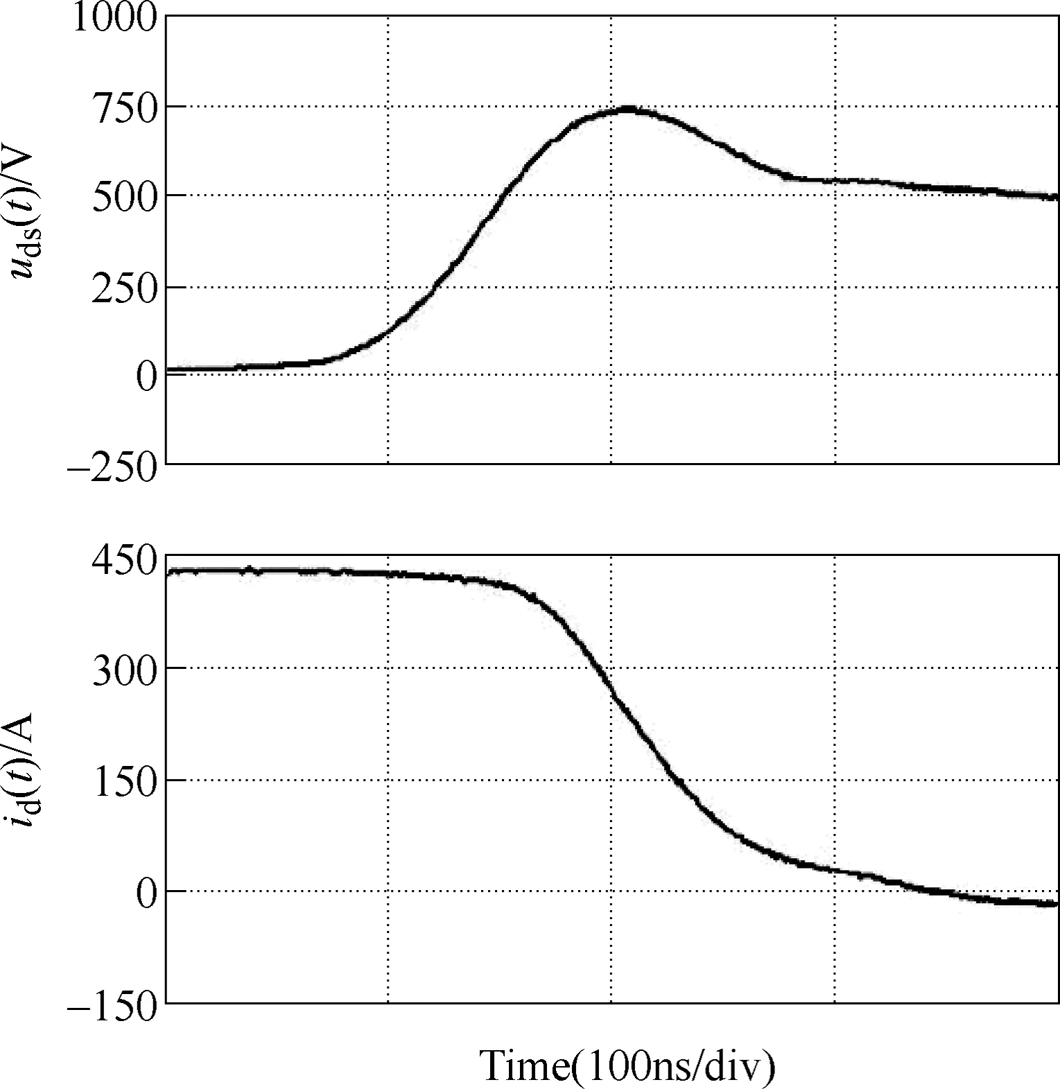
Fig.11 Experimental waveforms rated at 500V and 430A
On the other hand, the surge voltage at turn-off is 273V, which is 47.3% of the 500V DC voltage. That is,because the standardization impedanceZ% and surge voltage become equal, the parasitic inductance using the standardization impedance is clearly effective.
4 Electromagnetic noise caused by switching operations
The electromagnetic noise component caused by parasitic inductance includes a surge attributable to switching and an attenuation vibration component.Fig.12 shows the results of an experiment in which three types of bus bars were made with different structures and equal parasitic inductance. Table 2 shows the bus bar geometry and total stray inductance. In this case, the stray inductances of the three bas bars are the almost same, but the bus bar geometries are different. The results confirm that oscillation waveforms under turn-off operations differ regardless of whether the surge voltage is equal or not. This frequency component of the oscillation is the main component of the magnetic noise in power converter circuits and thus shows the indispensable necessity of wiring geometry design as a countermeasure to magnetic noise.
There are many papers assessing impact of parasitic inductance, but the phenomenon has still not been fully investigated, and only fragmentary results have been reported. There has still not been a comprehensive discussion covering both conductive and radiated noise;thus, these are topics for future research.
5 Conclusion
As advancements are made in power devices, it will become increasingly important for a geometry design focused on the parasitic inductance of power converter circuit. Normally, the wiring was treated merely as acomponent for connecting other parts with zero impedance, but in the future, it must be designed as a critical component for circuit implementation. In addition,power converter circuit design and development should not rely solely on trial and error and experience, but rather involve analysis and reflect the parasitic inductance. The parasitic inductance due to the wiring structure is a particularly important element in the design and manufacture of circuits using SiC and GaN power devices. Although this paper focused only on the parasitic inductance, the capacitor and power-module internal inductance are also important.

Table 2 Bus bar geometry and stray inductance
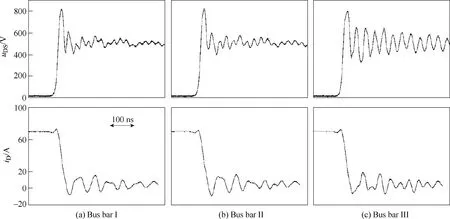
Fig.12 Experimental waveforms depending on bus bar geometry
 Chinese Journal of Electrical Engineering2018年3期
- Chinese Journal of Electrical Engineering的其它文章
- A Comprehensive Survey on Fault Diagnosis and Fault Tolerance of DC-DC Converters
- Active Thermal Control for Delaying Maintenance of Power Electronics Converters
- Reliability Analysis of Grid-Interfaced Filter Capacitors
- Capacitive DC Links in Power Electronic Systems-Reliability and Circuit Design
- Study of the Characteristics and Suppression of EMI of Inverter with SiC and Si Devices
- Design, Implementation and Performance of Synchronous Current Regulators for AC Drives
