Study of the Characteristics and Suppression of EMI of Inverter with SiC and Si Devices
*
(State Key Laboratory of Advanced Electromagnetic Engineering and Technology, School of Electrical and Electronic Engineering, Huazhong University of Science and Technology, Wuhan 430074, China)
Abstract: The paper systematically studies the impacts of two major factors: device switching actions and inverter switching frequency on the whole EMI spectrum. Several powerful experimental results of electromagnetic interference(EMI) in voltage source inverter(VSI) with SiC and Si devices are provided. As far as the influence of switching actions is concerned: faster switching speed will generate higher EMI noise levels in the high frequency range, and ringing in the device switching will also make the EMI noise near the ringing frequency range worse. In the meantime, increasing of the switching frequency of the inverter will result in a higher EMI noise peak for the whole EMI spectrum.In order to suppress the EMI noise of the converter to meet standards, Random PWM(RPWM) and EMI filters are adopted. With RPWM, the EMI current can drop a few more dB than that with SVPWM,which makes the filter work better. Also, as extra attenuation can be provided, it provides the benefit of reducing the weight and volume of the inductor of the filter. Therefore, the combination of an advanced modulation strategy and EMI filter is proposed for suppressing of EMI noise in an inverter.
Keywords: Motor drive, EMI, SiC, ringing, EMI filter, PWM.
1 Introduction
Electromagnetic interference(EMI) is a serious problem in many power applications especially for transportation applications like aerospace and vehicle systems. EMI can be with conductive high frequency currents or even higher frequency electromagnetic waves. EMI standards have been assigned to limit the EMI noise in applications. Use of an EMI filter is the most common approach to attenuate conducted EMI noise[1-2], but requires introducing extra components to the motor drive system. [3] has done a systematical study of EMI noise path for novel SiC based motor drives. With regards to noise source, [4] and [5] have studied the SiC device’s impact on noise source, but not with analysis for both switching actions and switching pulse series. This paper will give a comprehensive review of the physical principle of EMI noise for motor drive systems and provide powerful experimental results. At the same time, a new recommendation for suppression of EMI noise is proposed.
A typical topology of three-phase voltage source inverter(VSI) as the motor drive is shown in Fig.1(a).Because of continuous switching of power electronics devices in the VSI, high frequency EMI will conduct in both AC and DC sides. Fig.1(b) and Fig.1(c) are the equivalent circuits of AC side and DC side. In AC side in Fig.1(b), the VSI terminal voltages(Vao,Vbo,Vco) work as the EMI noise source. In DC side in Fig.1(c), AC side current is chopped by each phase-leg switching actions and together work as the EMI noise source.
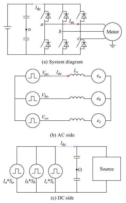
Fig.1 EMI conducting model in VSI based motor drive
The EMI noise sources of the AC side and the DC side have been defined by analysis. Both switching current and switching voltage are directly determined by the switching effects in the converter. In the timedomain, the EMI noise source is the chopped voltage or current series. The switching effects contain two major parts: firstly is the switching action of the devices and secondly is the switching pulse series as shown in Fig.2.Switching actions contain two factors: rise timeτrand fall timeτf. In fact, switching actions are contained in the pulse series, however, switching pulse series here only refer to the long time scale factors including switching frequencyfsand duty cycleD. Such a periodic pulse sequence with fixed amplitude of A is established in Fig.3.
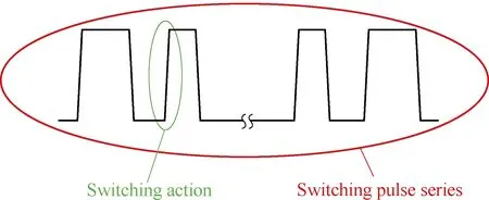
Fig.2 Chopped voltage or current series
By Fourier transformation, the spectrum in frequency domain is derived as formula (1) whenτr=τf.

Amplitude of thenth order harmonic (n>0) can be obtained as formula (2).

According ton=f/fs, the amplitude is shown in formula (3).

The envelope of the trapezoid wave is shown in Fig.4. It is clear that the envelope determined by switching actions (rise timeτrand fall timeτf) and switching pulse series (switching frequencyfsand duty cycleD), For a shorter rise timeτrh(higher switching speed), the envelope will shift right at high frequency ranges, resulting in more serious EMI noise issues at high frequency ranges.
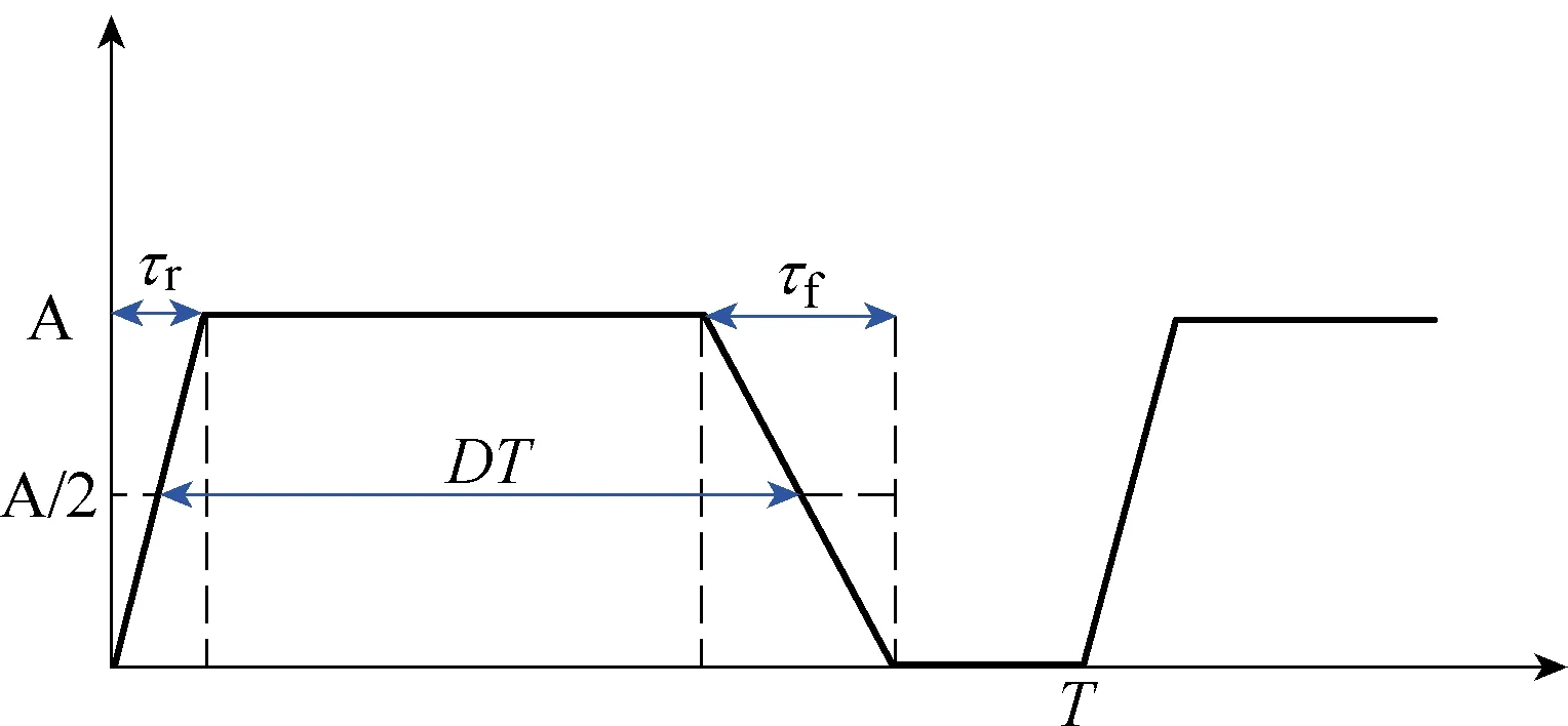
Fig.3 A periodic pulse sequence
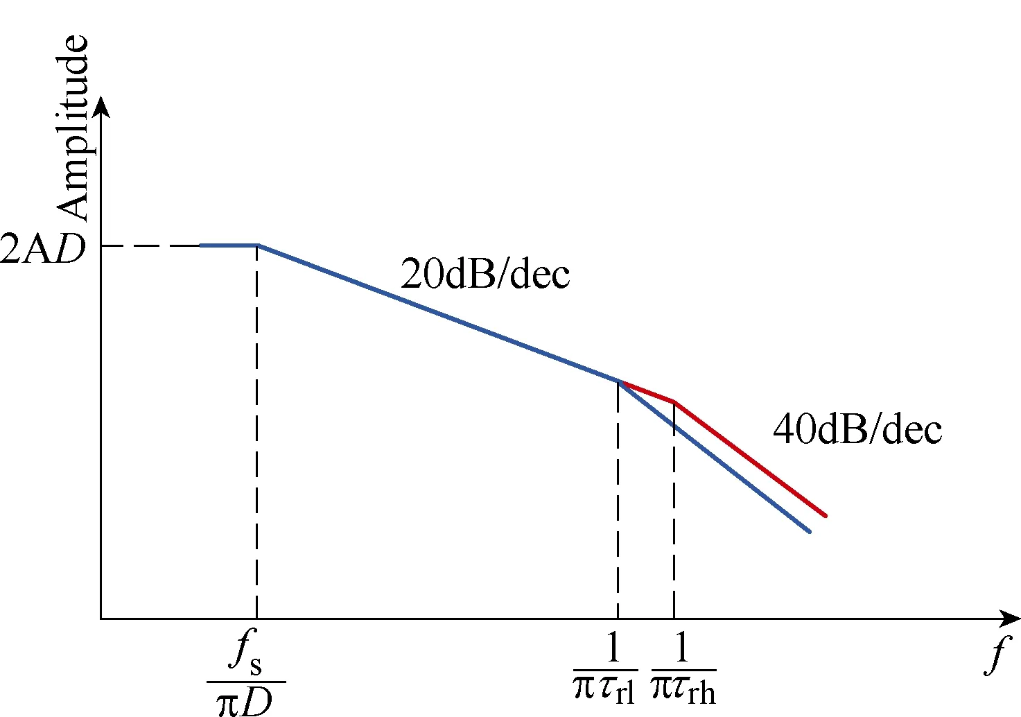
Fig.4 The spectrum of a periodic pulse sequence with different rise time
However, as it is always the case thatτris not equal toτf, the derivation will be more complex. The impact of real switching actions including differentτrandτfon EMI will be studied in the experimental results in the next section.
As shown in Fig.5, when the switching frequency increases fromfsltofsh, the spectral envelope will shift right at low frequency range and shift upwards at high frequency range, so the EMI of the whole spectrum will get higher.
In Fig.6, the whole spectral envelope shifts left and upwards when the duty cycle increases fromDltoDh,resulting in a more serious EMI noise issue at both low frequency range and high frequency ranges.
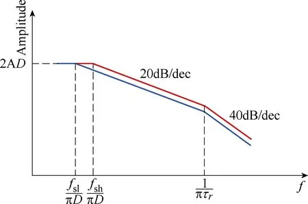
Fig.5 The spectrum of a periodic pulse sequence with different switching frequency

Fig.6 The spectrum of a periodic pulse sequence with different duty cycle

Fig.7 The double-integral Fourier analysis of 200V VSI with SVPWM
The phase-leg output voltage of VSI has a varying duty cycle instead of a fixed one, and the derivation of the spectrum envelope is very complex. [6]has given the double-integral Fourier analysis of voltage of VSI with SVPWM, without consideration of the switching actions. As shown in Fig.7, the carrier harmonic amplitude depends on the integer indicesn, independent of the switching frequency. Therefore, increasing the switching frequency will stretch and shift the spectrum without changing the harmonic amplitude at the same integer indices, so the EMI noise will get worse. Although the duty cycle is varying, a specific modulation strategy such as SVPWM has a fixed spectral envelope and the spectral envelope will be shifted as the switching frequency changes.
Therefore, for a specific modulation strategy,switching frequency of pulse series and switching actions of devices are two major factors determining the EMI noise of the converter.
For a typical EMI standard as shown in Fig.8, there are two main contributors. The switching actions with fast di/dt and dv/dt in the current/voltage source mainly contribute to the high frequency range. The switching frequency contributes to the whole EMI spectrum including the low frequency and the high frequency. The boundary of the two ranges is determined by rise time and fall time (switching speed).
Besides the EMI propagation equivalent circuit in Fig.1 with the main motor drive circuit loop for so called differential-mode(DM) EMI, common-mode(CM) EMI is an extra compontent of the whole EMI noise, which is conducted through the parasitic capacitors to the ground.For CM EMI, the noise source is the switching voltage,but for DM EMI, the noise sources are the switching voltage in AC side and the switching current in DC side.This paper is mainly focusing on the DM EMI of voltage source inverters with SiC and Si devices, both the suppression of DM EMI in AC side and DC side will be discussed.
Fig.9 shows two inverters designed with a modular approach[7-9]. The only difference between the two is the power electronic devices. SiC devices used in this paper are 1200V JFETs (IJW120R100T1) and 1200V SBDs(IDW40G120C5B) from Infineon. Si devices used to make a comparison in this paper are 1200V IGBTs(IKW40N120H3) and fast switching diodes (IDP30E120)from Infineon. Three phase-leg modules are shown in Fig.10.

Fig.8 Frequency range for a typical EMI standard
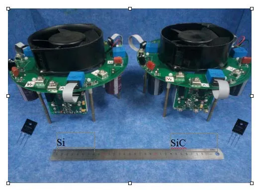
Fig.9 Two inverters designed with different devices
In this paper, the analysis above will be further verified by experiments, the impact of switching actions on EMI is discussed in Part 2 and the impact of switching frequency on EMI is discussed in Part 3. Then,solutions of the system EMI mitigation are presented in Part 4. Conclusions are summarized in Part 5.
2 Impact of switching action on EMI
As mentioned in the introduction, the switching actions determine the EMI at high frequency ranges.Also, the fast switching speed will form a ringing through the parasitic parameters in the circuit. Ringing phenomenon will also be studied for EMI in this section.
2.1 Impact of switching speed
A phase-leg module with Si IGBTs and a phase-leg module with SiC JFETs and SBDs are compared with their switching waveforms by double-pulse-test,and experimental results are illustrated in Fig.11. SiC phase-leg module has a faster switching speed and with less reverse-recovery based over-shoot current, as shown in Fig.11. This kind of phenomenon happens in every switching process for the motor drive, and influences the EMI noise of the whole system. Similar phenomenon can also be found in the voltage switching waveforms.
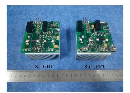
Fig.10 Phase-leg modules
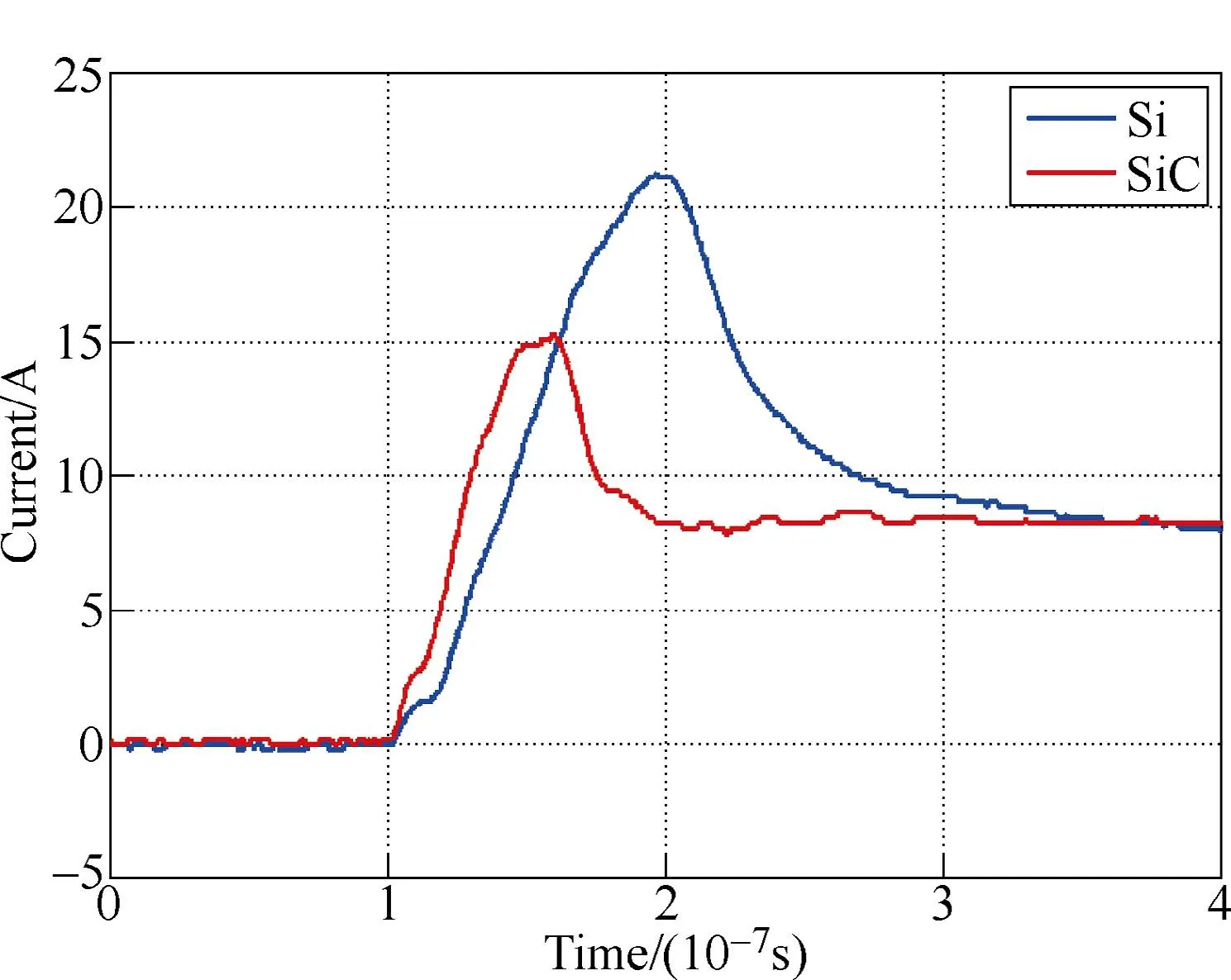
Fig.11 Experimental results analysis of switching waveform (cites from Fig.7 in [10])

Fig.12 Experimental results of EMI current of VSI with different switching devices
The difference in the single switching action will impact the EMI of the inverter. Fig.12 is the experimental result of the EMI current of inverter with the same load as captured by the EMI test receiver. Both SiC devices and Si devices are switching with 20kHz by SPWM to ensure the impact of switching pulse series on EMI are the same for the two cases and the comparison of devices’ switching actions is fair. It is clear that the peak of the red curve is higher than the blue curve when amplifing the results of the high frequency range, 5~30MHz in this case. But the two curves match well at the low frequency range. This indicates that the switching actions indeed mainly determine the EMI current at high frequency ranges, where the faster the switching speed (shorterτrandτf), the more serious the EMI.
2.2 Ringing’s impact
For SiC devices, which significantly increase the switching speed, parasitic parameters in the commutation loop can bring resonance and ringing in the switching waveform. Reference [11] has done a study of the parasitic inductance’s influence on the switching waveform ringing. Reference [12] has proven that ringing will make the EMI of a converter worse,but it does not elaborate on the physical principle. By artificially adding an air core inductor to the switching loop, ringing will happen in the switching waveform,shown in Fig.13.

Fig.13 Add air core inductor to the switching loop
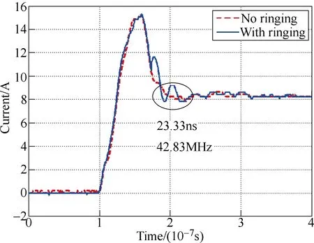
Fig.14 Experimental result of ringing’s influence on switching waveform

Fig.15 EMI comparison for the case with and without ringing in experiments
Fig.14 shows experimental results of the comparison of switching current between with and without ringing.The ringing is associated with ~40MHz. With the EMI test receiver, EMI comparison is shown in Fig.15, for the case with and without ringing. As shown in the experimental result of EMI test receiver, the ringing is associated with ~40MHz and the measured corresponding frequency range is 40MHz to 60MHz at which the EMI noise is worsened. Therefore, ringing which may occur in the switching action will worsen the EMI noise at the frequency range corresponding to the ringing time scale,although the range usually belongs to the radiation EMI.
3 Impact of switching frequency on E MI
As mentioned in the introduction, switching frequency is another dominating factor for a specific modulation strategy such as SVPWM.
For a typical three phase inverter withR-Lload, the DC bus voltage is 400V, Si devices switch withfsof 20kHz and for the same inverter, SiC devices switch withfsof 50kHz, experiments have been done. The measured conductive EMI current comparisons in AC and DC side are shown in Fig.16 and Fig.17.
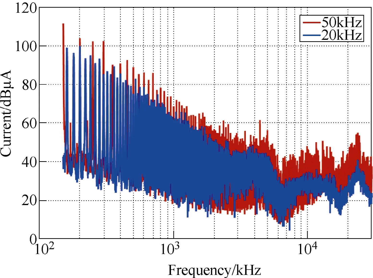
Fig.16 Experimental results of EMI current in AC side
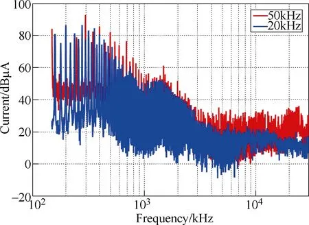
Fig.17 Experimental results of EMI current in DC side
The EMI noise for an SiC based inverter is clearly higher than that of an Si based inverter because of the higher switching frequency, for both the AC and DC side.This is consistent with the results of theoretical analysis in the introduction. For EMI high frequency range, the system's EMI not only depends on the switching frequency, but also the switching actions. Therefore, the EMI current of the SiC based inverter at high frequency range is much higher than the Si based inverter due to the higher switching frequency and the faster switching speed.
4 Solutions to the system EMI mitigation
With the characteristics of EMI in a voltage source inverter clarified in Part II and III, the solutions for EMI mitigation are discussed. For the moment, the solutions mainly include advanced EMI reduction modulation strategies and EMI filtering. The suppression ability of an advanced EMI reduction modulation strategy on EMI is usually limited between 10dBμA and 20dBμA.Although the suppression ability of EMI filter is unrestricted, it requires some passive components which take a significant portion of the total volume and weight of the converter[13-15].
4.1 EMI reduction modulation strategy
Some of the advanced EMI reduction modulation strategies depend on special topology to reduce EMI noise source. Some modulation strategies reduce EMI noise by keeping the mean switching frequency with a certain range of the variation, such as variable switching frequency pulse width modulation(VSFPWM)[16]and random pulse width modulation(RPWM)[17-20]. Both of these can distribute the EMI energy peak near the integer indices of switching frequency to a wider range. The variable frequency range of RPWM is determined by the level of randomness, but the variable frequency range of VSFPWM is mainly determined by the circuit parameters and modulation index, and as such the change of variable frequency range of the former is more flexible.
Fig.18 shows the process of implementation of RPWM: in the controller, saving a buffer with multiple random numbers. Once the duty cycle is determined in each interruption period, updating the switching cycleTswith a random number, then the long-period switching cycle can be randomly distributed.

Fig.18 Process of implementation of RPWM
The switching frequency variation range can be controlled as shown in (4). The random numbers in the buffer rand [N] are within the range of -1~1. By controlling the coefficientλ, the switching frequency can be limited. This method can make the average switching frequency of RPWM close to the constant switching frequency PWM and the comparison to be fair.

For switching loss consideration, the Si based inverter(fs=20kHz) has a switching frequency variation range between 15kHz and 25kHz and the SiC based inverter(fs=50kHz) has a switching frequency variation range between 37.5kHz and 62.5kHz. Experimental results are shown in Fig.19 and Fig.20. If RPWM modulation strategy is used, a limited suppression of about 10dBμA is provided in AC side. When comparing the results of RPWM, it is clear that the DM EMI current of SiC based inverter dropped more than the Si based inverter for the wider variation range of switching frequency. However, the SiC based inverter with higher average switching frequency still generates higher EMI noise than the Si based inverter.
4.2 DM EMI filter for both AC side and DC side
For AC side EMI of the inverter, as discussed in part I, the EMI noise source is the switching voltage.The single-phase EMI conductive model is shown in Fig.21, considering the equivalent paralleled resistor(EPR) and equivalent paralleled capacitor(EPC) of the filter inductor and the equivalent series resistor(ESR) and equivalent series inductor(ESL) of the filter capacitor.
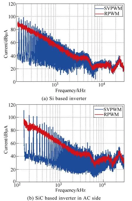
Fig.19 Experimental results of EMI current

Fig.20 Experimental results of EMI current
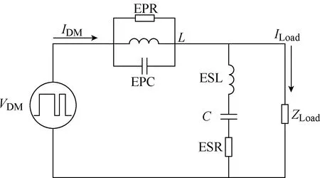
Fig.21 Frequency domain model of a typical VSI in AC side
Fig.22 shows a comparison of EMI standard and EMI noise in AC side of SiC and Si based inverters.According to the attenuation required to drop the EMI current below the standard, the cut-off frequency and inductance of the filter are calculated when the capacitance is equal to 1.5μF. For time and cost considerations, the inductor cores used in this paper are the off-the-shelf toroid cores instead of customized, and the inductance of the filter is then limited by the size of the core. A one-stage EMI filter is used for Si based inverter without a margin of 6dB. A two-stage EMI filter has to be used for an SiC based inverter because of the bigger EMI noise and the small core. The inductance of each stage is reduced, where then a margin of 6dB can be added to the EMI filter for the SiC based inverter.Calculated parameter values of EMI filter on the AC side is shown in Table 1.
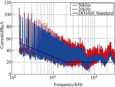
Fig.22 Comparison of EMI standard and EMI noise in AC side of Si based inverter and SiC based inverter
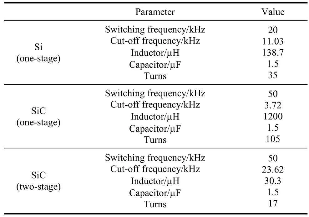
Table 1 Calculated parameter values of EMI filter in AC side
Fig.23 shows the filters designed for Si and SiC based inverters. The two-stage filter for the SiC based inverter (50kHz) is clearly heavier and more bulky than the one-stage filter for the Si based inverter (20kHz).The EMI current in AC side before and after adding DM LC filter of Si and SiC based inverters is shown in Fig.24 and Fig.25. The EMI filter for an Si based inverter does not fully met the requirements for lacking a margin and the existence of the parasitic coupling[21-24].The EMI filter for SiC based inverters makes the EMI current for all frequency ranges fall below the standard.
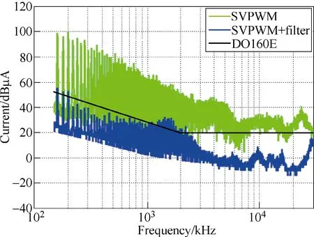
Fig.24 EMI current in AC side before and after adding filter of Si based inverter
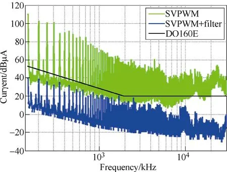
Fig.25 EMI current in AC side before and after adding filter of SiC based inverter
The insertion loss of the filter for an Si inverter is inadequate as seen in Fig.25. In order to further increase the insertion loss of the filter, a larger inductance can be used increasing the weight and volume of the filter.However, if the EMI reduction modulation strategy RPWM instead of SVPWM is based on use of an existing EMI filter, an extra attenuation will be added without increasing weight and volume of the filter, and the system EMI current will drop below the standard more easily as shown in Fig.26, as it makes up for the inadequate attenuation of the designed filter. In addition,if RPWM is based on use of an existing EMI filter for an SiC inverter, the EMI current of the system will drop lower than the standard as shown in Fig.27. As an extra 10dB attenuation is provided, the filtering result is much better with a reduced volume and weight, or it is not required to reserve a margin of the EMI filter, which allows for EMI filters to be lighter and smaller.Therefore, when the EMI filter is necessary for the system, the combination of an advanced modulation strategy, i.e., not just RPWM is proposed, without affecting system performance and EMI filter.

Fig.26 EMI current in AC side before and after adding filter with SVPWM and RPWM of Si based inverter

Fig.27 EMI current in AC side before and after adding filter with SVPWM and RPWM of SiC based inverter
In fact, comparisons between parameter values of filter for inverter with RPWM and with SVPWM can be made according to their corresponding EMI noise as shown in Fig.19 (the blue curve and red curve). The cut-off frequency of EMI filter increases for both Si and SiC based inverters with RPWM. As a result, the value of inductance and the turns of the core both reduce in Fig.28, for example 138.7μH vs 73.2μH and 612.3μH vs 127.3μH of inductor, 35 vs 25 and 74 vs 34 of turns. The EMI noise of SiC based inverter (37.5kHz to 62.5kHz)is reduced more than that of Si based inverter (15kHz to 25kHz) due to a wider variable frequency range, so the inductor decreases from 612.3μH to 127.3μH, and the turns decreases from 74 to 34, which is more than 50%.Nevertheless, the inductance of EMI filter for SiC based inverters(50kHz) is still bigger than that for Si based inverters(20kHz), in this case whether the modulation strategy SVPWM or RPWM is adopted, for 612.3μH vs 138.7μH and 127.3μH vs 73.2μH, unless the cut-off frequency can be further decreased.
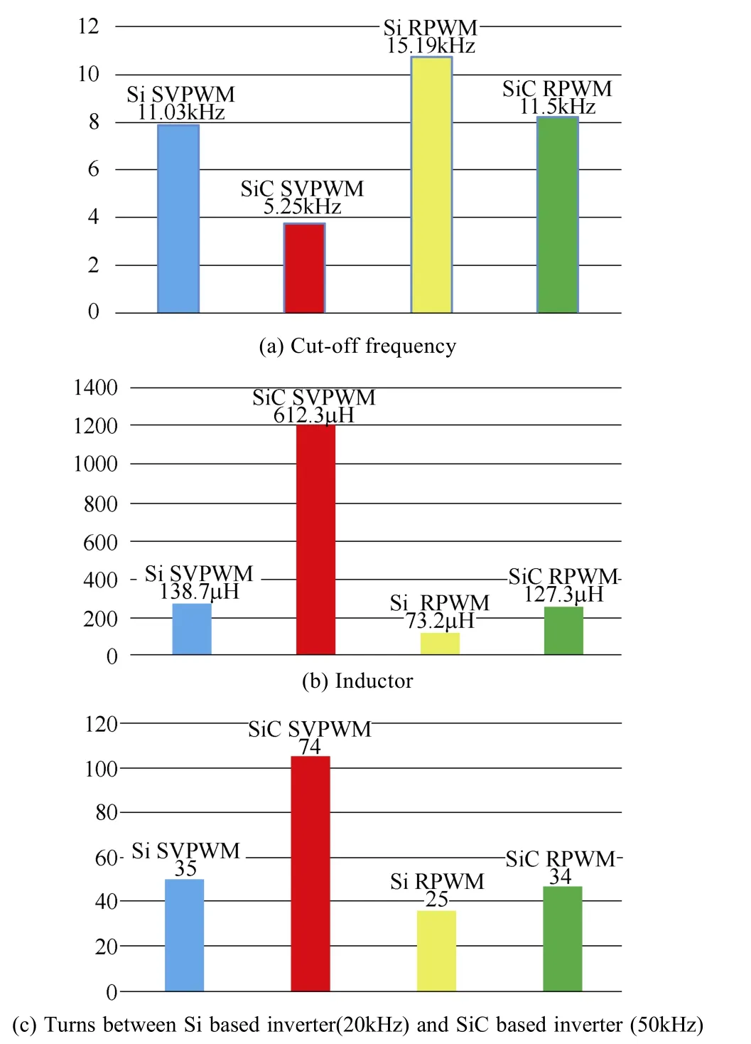
Fig.28 Result Comparison
Fig.29 shows the comparison of the size of inductors. The core of one-stage EMI filter for Si based inverter can be lighter and smaller with RPWM. What’s more, though the baseline EMI noise of an SiC based inverter is much more of an issue because of the higher switching frequency, the two-stage filter for the SiC inverter can be replaced by a smaller one-stage filter when RPWM is used instead of SVPWM.
Fig.30 is the frequency domain model of a typical inverter in the DC side. The calculated parameter values of EMI filters in DC side are shown in table 2.
Fig.31 and Fig.32 show that in the DC side, the filter does not achieve the best filtering result either for Si or SiC based inverters. However, if RPWM is used instead of SVPWM, the EMI filters work much better as shown in Fig.33 and Fig.34. It is similar to the AC side that the combination of the two can make up for the inadequate attenuation of the EMI filter to achieve a better filtering result.
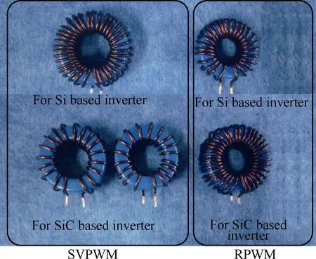
Fig.29 Inductor of EMI filter for Si based inverter and SiC based inverter with SVPWM and RPWM in AC side

Fig.30 Frequency domain model of a typical VSI in DC side

Table 2 Calculated parameter values of EMI filter in DC side

Fig.31 EMI current in DC side before and after adding filter of Si based inverter

Fig.32 EMI current in DC side before and after adding filter of SiC based inverter
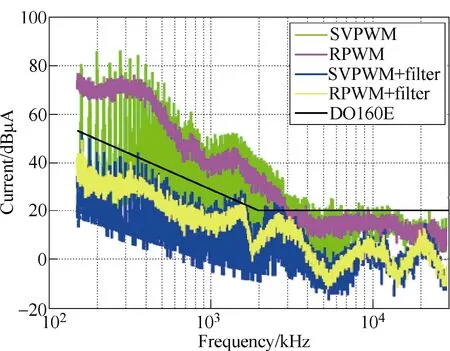
Fig.33 EMI current in DC side before and after adding filter with SVPWM and RPWM of Si based inverter

Fig.34 EMI current in DC side before and after adding filter with SVPWM and RPWM of SiC based inverter
5 Conclusion
The application of SiC devices in motor drives can significantly improve efficiency and dynamic performance,and in addition, their superior capability can increase the power density of the motor drives and making the high speed motor controller a possibility. However, the challenge of more serious EMI levels also appears. The paper systematically reviews the impacts of two major factors: device switching actions and inverter switching frequency on the whole EMI spectrum. Through analysis and experimental results, a few conclusions can be obtained.
First, the cause of EMI in inverter has been claimed:the switching actions and the switching frequency are the two major factors affecting the conduction EMI of a converter with a specific modulation method.
Switching actions affect EMI noise at high frequency range. For SiC devices, their fast switching speed will create more EMI noise in high frequency ranges. Meanwhile, if parasitic parameters in the commutation loop bring ringing in switching, it will make increase the EMI noise at the corresponding frequency range.
Switching frequency affects EMI noise within the range of the whole EMI spectrum. For SiC based inverters with higher switching frequency, the EMI noise will get worse and the resulting EMI filter is usually more bulky.
In order to suppress the EMI noise of the inverter,an advanced EMI reduction modulation strategy and EMI filter are adopted in this paper. Modulation strategy such as RPWM has a limited attenuation of about 10dB without adding any extra components to the system. The combination of an advanced modulation strategy and EMI filter makes a more superior EMI filter.
 Chinese Journal of Electrical Engineering2018年3期
- Chinese Journal of Electrical Engineering的其它文章
- A Comprehensive Survey on Fault Diagnosis and Fault Tolerance of DC-DC Converters
- Active Thermal Control for Delaying Maintenance of Power Electronics Converters
- Reliability Analysis of Grid-Interfaced Filter Capacitors
- Capacitive DC Links in Power Electronic Systems-Reliability and Circuit Design
- Circuit Implementation of Power Converter for High-Speed Switching Operations
- Design, Implementation and Performance of Synchronous Current Regulators for AC Drives
