Capacitive DC Links in Power Electronic Systems-Reliability and Circuit Design
(Center of Reliable Power Electronics, Department of Energy Technology,Aalborg University, Aalborg 9220, Denmark)
Abstract: Capacitive DC links are an important part in voltage source power electronic converters,which contribute to cost, size and failure rate on a considerable scale. With more and more stringent constraints brought by industrial applications, the capacitive DC links encounter reliability aspect challenges. This paper presents a review on the reliability design and improvement of capacitive DC links from three aspects: 1) Quantitative reliability prediction for DC-link capacitors; 2) Reliabilityoriented design of passive DC-link capacitor banks; and 3) Advanced active DC links to exceed the limits of passive DC-link capacitors. Key solutions for each aspect are highlighted and discussed with case studies. This review serves to provide a picture of state-of-the–art research on the reliability design and improvement of capacitive DC links, highlight the key milestones in this area, and identify the corresponding challenges and future research directions.
Keywords: Reliability, capacitor, DC link, power electronics.
1 Introduction
Capacitive DC links are widely used in power electronic systems to filter the harmonic currents, buffer the instantaneous power difference between the input source and output load, and minimize the voltage variation in the DC link[1]. In three-phase applications such as Adjustable Speed Drive(ASD), and Wind Turbine(WT) systems, the instantaneous power is six times that of the fundamental frequency under grid voltage balanced condition, and two times that of fundamental frequency under unbalances[2-3]. In single-phase rectifier or inverter applications such as Photovoltaic(PV), and Fuel Cell(FC) system, the conversion between DC and AC power will typically introduce a double fundamental frequency pulsation power and ripple voltage harmonics at the DC link of the power conversion system[4]. The low-frequency voltage harmonics are detrimental to the DC side utility of the converter, deviate Maximum Power Point Tracking(MPPT) in a renewable energy system, and impact the power quality and reliability of the power grid[5-6]. In order to decouple the impact between the two stages connected through DC links, capacitive DC links are applied.
The most commonly used passive DC links are capacitive ones, which are one of the highest failure rate components in power electronic systems and contributes to more than 20% failures in certain applications[7].From the system-level aspect, capacitor is the bottleneck of the power electronic systems[8]. The failure probability contribution of a DC-DC converter system discussed in[8] is shown in Fig.1. It reveals that the DC-link capacitors contribute to the highest failure probability among other components and mostly determine the lifetime of the power electronic system.
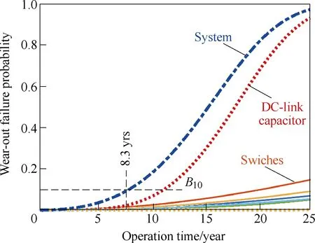
Fig.1 Failure probability of components and system in a DC-DC converter application[8]
With more stringent reliability constraints brought by automotive, aerospace, and energy industries, the design of DC links encounters the following challenges[1,9]:①Capacitors are one kind of the stand-out components in terms of failure rate in field operation of power electronic systems; ②Cost reduction pressure from global competition dictates minimum design margin of capacitors without undue risk; ③Capacitors are to be exposed to more harsh environments (e.g., high ambient temperature, high humidity, etc.) in emerging applications,and ④Constraints on volume and thermal dissipation of capacitors with the trends for high power density power electronic systems.
From the capacitor end-user perspective, the effort of overcoming the challenges can be divided into three categories which are reviewed in this paper: ①Electrothermal-lifetime modeling to support model-based sizing of capacitors[10-15]; ②Multi-objective optimization of passive capacitor banks in terms of cost, size, efficiency,and reliability[16-19]; ③New capacitor concepts based on active switching circuits[20-35]. The first effort is an analysis tool to predict the reliability performance of the capacitive DC links. Based on the reliability assessment,the reliability-oriented design and optimization solutions for the applied passive capacitor bank can be provided.In the third effort, active DC links with power electronic circuit to exceed the physical limits of the passive DC-link capacitors are reviewed. The challenges and opportunities for future research direction are finally addressed.
The structure of this paper is as follows: Section 2 presents the reliability prediction of capacitors with physical of failure understanding; Section 3 and 4 present the advanced technologies for reliability improvement in terms of passive and active DC links,followed by the conclusions.
2 Lifetime prediction of DC-link capacitors
DC-link capacitors can fail due to intrinsic and extrinsic factors, such as design defect, material wearout, operating temperature, voltage, current, moisture,mechanical stress, and so on. Generally, the failures can be divided into catastrophic failures due to single-event overstress and wear-out failures due to the long-term degradation of capacitors. The state-of-the-art methods for lifetime prediction of capacitors for the wear-out failures can be divided into two categories: lifetime prediction for constant operating condition and lifetime prediction for long-term mission profile.
2.1 Lifetime prediction for constant operating condition
For the constant operating condition, lifetime prediction with a simplified lifetime model is commonly used in power electronic applications. The most widely used lifetime model for capacitors is shown in (1), which describes the influence of temperature and voltage stress[1]:

whereLandL0are the lifetime under the using condition and testing condition, respectively.VandV0are the voltage at use condition and test condition, respectively.TandT0are the temperature in Kelvin at use condition and test condition, respectively.Eais the activation energy,KBis Boltzmann’s constant 8.62×10⁻⁵eV/K, andnis the voltage stress exponent. Therefore, the values ofEaandnare the key parameters to be determined in the above model. In [36], theEaandnare found to be 1.19 and 2.46, respectively, for high dielectric constant ceramic capacitors. In [37], the ranges ofEaandnfor MLC-Caps are 1.3~1.5 and 1.5~1.7, respectively. The large discrepancies could be attributed to the ceramic materials, dielectric layer thickness, testing conditions,etc. With the trend for smaller size and thinner dielectric layer, the MLC-Caps will be more sensitive to the voltage stress, implying a higher value ofn. Moreover,under different testing voltages, the value ofnmight be different as discussed in [38].
2.2 Lifetime prediction for long-term mission profile
In the above lifetime prediction method shown in section 2.1, the operating condition is assumed to be constant. However, in real power electronic applications,the conditions are always changing with the environment(e.g., ambient temperature, relative humidity and vibration), user’s behavior (e.g., loading conditions and input variations) and the status of the system itself (e.g.,parameter variation and devices degradation)[11].
In recent years, lifetime prediction for long-term mission profile has been proposed[8-11]. Differing from the lifetime prediction in constant operating condition,this method takes into account the long-term and variable loading conditions. Furthermore, various sources of uncertainties exist (e.g., tolerances in component parameters, modeling errors) Therefore, a statistical approach based on Monte-carlo simulation is applied[39].Compared with the method in section 2.1, the lifetime prediction for long-term mission profile is more closely related to the real operating condition. The lifetime estimation procedure is shown in Fig.2. It includes three major steps: electro-thermal loading analysis, damage accumulation, and Monte-carlo simulation based variation analysis. A mission profile (i.e., ambient temperature,loading condition) is applied as the input. The output is the lifetime of the capacitor with a certain confidence level (e.g., 90 %).
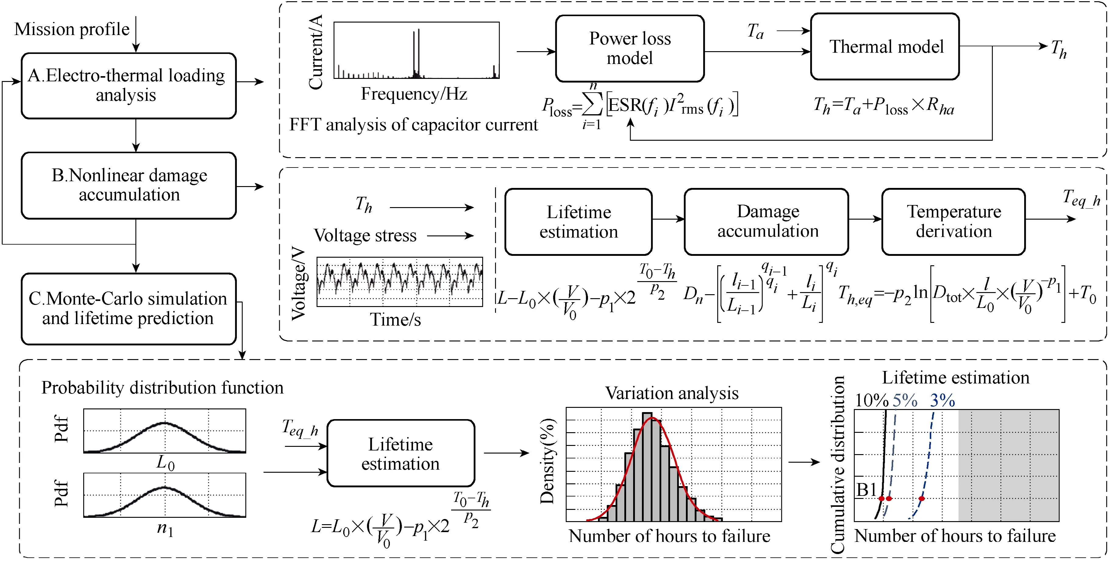
Fig.2 Mission profile based lifetime prediction procedure[11]
2.2.1 Electro-thermal loading analysis
Thermal stress is critical to capacitor wear out. The ripple current and ambient temperatures are the contributors to the capacitor hot-spot temperature. For electrolytic capacitors, the dominant degradation mechanisms are electrochemical reaction in the oxide layer and the electrolyte vaporization[40-41]. The thermal stress leads to an increase of Equivalent Series Resistor(ESR) over time. In particular, the increase of capacitor power loss causes a higher operating temperature inside the capacitor. The hot-spot temperature of the capacitor,which is effected by the current stress and ambient temperature, is presented by [11]

whereThis the hot-spot temperature,Tais the ambient temperature,Rhais the equivalent thermal resistance from hotspot to ambient, ESR(fi) is the equivalent series resistance at frequencyfi,Irms(fi) is the RMS value of the ripple current at frequencyfi.
2.2.2 Damage accumulation
The linear and nonlinear accumulated damage model is developed to describe the real damage progress[11,13]. The wear out of the capacitor is indicated by an increase of ESR. Damage is then defined as the ratio of instantaneous to final ESR growth. As an example, the formulated nonlinear model that accounts for the effects of these processes, but without a specific identification and is represented by

qis a function of lifetimeLand material constants.liandLiare the instantaneous equivalent operating time and total lifetime under the same loading condition,respectively. By accumulating the damage, the dynamical stresses are converted into static values for each type of temperature stress. Taking the accumulated damage into the lifetime model, the equivalent hot-spot temperature can be derived.
2.2.3 Monte-Carlo analysis and lifetime prediction
The application of the lifetime model results in a fixed accumulated damage. It is far from reality since the capacitor parameter variations and the statistical properties of the lifetime model are ignored. In field operations, the time to end-of-life for the capacitors could vary within a range due to the tolerance in physical parameters and the difference in the experienced stresses.Therefore, a statistical approach based on Monte-carlo simulation is applied[8-11]. The sensitivity of the lifetime to temperature tolerance-related parameters can be evaluated individually or collectively. Finally, the distribution of the end-of-life of the capacitors can be obtained, allowing a lifetime analysis with a specified confidence level.
2.2.4 Closed-loop modelling process
Along with the damage accumulation, the capacitance reduction and ESR increase lead to an increasing of DC-link voltage ripple and changing of DC-link current,which accelerate the degradation process of the capacitor.A feedback loop is considered in the lifetime prediction procedure to represent the accelerated degradation.
3 Advanced passive DC links-reliability oriented design for capacitor banks
For the applications where single capacitor cannot fulfill the voltage rating or capacitance requirements,capacitor bank is always used as the energy buffer by connecting several capacitors in parallel for larger capacitance, or in series for higher voltage rating. In the ultra-compact converters with cost constraints, there are some design challenges for the capacitor banks:①Uneven temperature distribution among the capacitors inside the bank due to thermal coupling and uneven boundary conditions, which leads to a part of capacitors severity aging[17-19]. The temperature estimation based on a single capacitor becomes over-simplified; ②Longlifetime series of capacitors can be used to improve the reliability of the capacitor bank, however, at the expense of compromised performance in cost, power density,etc.[40-41].
At the beginning of reliability-oriented design,thermal loading distribution of the capacitor bank needs to be predicted, so as to acquire the lifetime of individual capacitor. Considering the self-heating and thermal coupling effects, the lumped thermal model of the capacitor bank can be written in the matrix form as[18]

whereTi(i=1,2…m) is the monitoring point temperature,Ploss,jwith (j=1,2…n) is the power losses of each capacitor,Ta,i(i=1,2…m) is the ambient reference temperature at the monitoring points, andZi,j(i=1,2…,mandj=1,2…n) is the coupling thermal impedance between the monitoring point and the reference point.In particular,Zi,j(i=j) is the self-heating thermal impedance.
From the lifetime model shown in (1), it can be seen that the rated lifetime, voltage stress and thermal stress are the key factors affecting the capacitor lifetime.Worth being noted is that if the voltage stress is under the rated voltage, it will introduce negligible effect on the lifetime. Therefore, design variables considered in this paper are the rated lifetime and thermal stress of each capacitor[18].
3.1 Lifetime matching of individual capacitors
Capacitor manufactures provide products with different classes of rated lifetime. The useful lifetime of capacitors is dependent on both its rated lifetime and the actual stress conditions. In a capacitor bank with multiple capacitors, the thermal coupling among the capacitors varies with physical location. The electrothermal stresses among individual capacitors may be different, thereby. One way to match the lifetime of the individual capacitors is by selecting capacitors with different rated lifetime to configure the capacitor bank.The optimized variables are the rated lifetime of individual capacitorLrated,1,Lrated,2, ...,Lrated,m, and the optimization target is to minimize the lifetime difference among capacitor cells, where the mathematical model are shown below[18]:
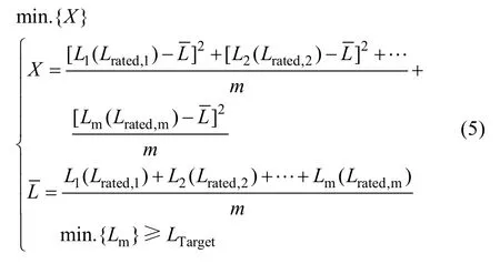
Xis the temperature variance.LmandLrated,mare the lifetime and the rated lifetime of the individual capacitorm, respectively.LTargetis the lifetime target of the capacitor bank.
A capacitor bank with nine electrolytic capacitors connected in parallel is used as a case study[18]. For conventional solution, 2000 hours rated lifetime series products are used for all individual capacitors. Based on the lifetime prediction shown in section 2.1, the lifetime of individual capacitor can be obtained, where the shortened lifetime of capacitor is a 4.7 year lifetime only at the middle of the capacitor bank, which cannot reach the 5 year lifetime target as shown in Fig.3. Based on the lifetime matching method, 3000 hours rated lifetime series product is used for the middle capacitor in the hybrid bank. Therefore, all the capacitors can satisfy the 5 year lifetime target with a slight rise in cost.
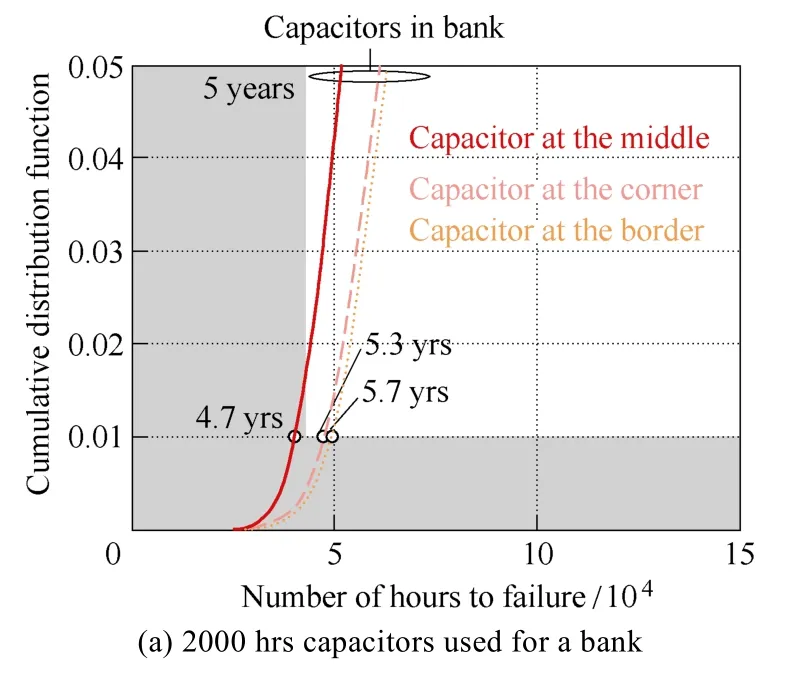
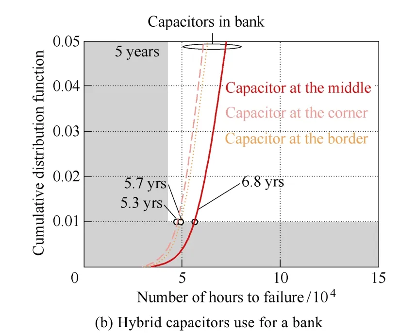
Fig.3 Lifetime estimation results with conventional design and hybrid design capacitor banks
In Fig.3(a),conventional design: individual capacitor uses 2000hours rated lifetime product, so that the capacitor at the middle has a 4.7 year lifetime which is lower than the 5 year. In Fig.3(b), hybrid design:partial capacitors use a 3000 hours series product for the middle capacitor and the others use 2000 hours series product, so that all the capacitor can reach 5 years lifetime target[18].
3.2 Thermal stress matching
Power loss is the source for the thermal stress,which is determined by the current spectrum and the ESR of each capacitor. The current spectrum at low-frequency bandwidth depends on the capacitance(or impedance at specified frequency) of the capacitor,because of current sharing among capacitors. The specified capacitor current can be obtained as

wherenis the number of capacitors in a bank,kis thek-th capacitor in the bank,Cnis the capacitance, andiBankis the total current of the capacitor bank. ESR is also related to the capacitance, which is given by [40]

where tanδis the Dispassion Factor(DF) andδis the loss angle. Based on (7) and (8), the power loss of thek-th capacitor can be derived as

It can be seen that the power loss of the capacitor is linear with capacitance. Therefore, the hot-spot temperature can be obtained based on the power loss and the proposed lumped thermal model. Worth being noted,in the same series products, the size normally changed with the capacitance, which will further affect the thermal impedance because of the variation of the heat spread area. Therefore, the temperature redistribution method should hybrid different downsize series products,which series provides different capacitances for the same size for a capacitor bank. Therefore, the power loss is the only variable corresponding to the hot-spot temperature as well as the lifetime of individual capacitor. The optimization model is defined as
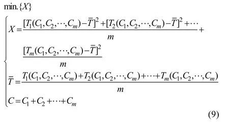
where the optimized variable is the capacitance for individual capacitor in the bank.
A case study is presented in Fig.4. With the same capacitance 470μF/450V for individual capacitor,the thermal loading distribution is uneven. Based on the proposed thermal stress matching method, the capacitance for individual capacitor can be optimized to balance the temperature, where four 750μF/450V, four 620μF/450V and one 390μF/450V capacitors are used.The total capacitance of the optimized solution is the same as with the design target and the cost keeps at a comparative level.
4 Advanced active DC links-two-terminal active capacitor
4.1 Overview of active DC links
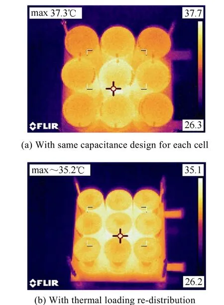
Fig.4 Experimental results of a capacitor bank without and with thermal stress matching solution
To exceed the limits of power density, capacitance,voltage rating, reliability, and cost, various new capacitor concepts with the aid of active switching circuits have been proposed. The majority of the applications are for DC links, i.e., active DC links.Active DC links are achieved by switching devices and significantly reduced passive components (e.g.,capacitors, inductors, or both)[20-35]. Its performance depends largely on the active switching circuits and less on the dielectric materials and manufacturing constraints as the passive capacitors. It provides a new perspective to optimize the reliability, cost, or power density less compromised constraints compared to conventional passive capacitor bank design.
The typical active DC link configurations are shown in Fig.5[25].ABis the DC terminal of the main circuit andCDis the AC terminal.AauxBauxis the input terminal of the auxiliary circuit andCauxDauxis the output terminal. An energy storage element is connected with the output terminal to balance the instantaneous power. Because the buffer capacitor is not directly connected with the DC link having a voltage-ripple constraint, the buffer capacitor can be reduced to allow large voltage ripple. Figs.5(a)~(c) show the solutions connected in series with the main circuit on the DC side.When there is ripple current flowing through the DC-link capacitor, the auxiliary circuit will generate a voltage ripple in order to minimize the DC-link voltage ripple ratio for system specification. Fig.5(d) shows the auxiliary circuit connected in parallel with the main circuit on the DC side. If there is ripple current on the DC link, the auxiliary circuit can be implemented as a current source to compensate the current directly. Therefore, no current and voltage ripple can be observed on the DC link ideally. Figs.5(e) and 5(f) present the auxiliary circuit connected with the main circuit in series and parallel on the AC side. The instantaneous power can be compensated directly on the AC side by instantaneous power calculation, mitigating the ripple on the DC side.
Following the topology derivation method in [25],different topologies with active DC links can be obtained based on the general structures in Fig.5.
4.2 A two-terminal active capacitor
Although many active DC links have been proposed in recent decades, they are rarely used in commercial products because of issues with cost, efficiency, and complexity. In order to make an active DC link more practical, a two-terminal active capacitor is proposed with the same level of convenience in use as passive capacitors and the feasibility in achieving better performance in cost, reliability, and/or power density[23].
The two-terminal active capacitor has the following features: ①Has two terminals only without any additional connection because of the proposed control method and the applied self-power circuit, making it possible to be packaged as a conventional capacitor from the end-user’s perspective, and ②Has impedance characteristics equivalent to a bulky capacitor or as a variable capacitor within a certain range of frequency depending on the control and switching frequency of its active switches for applications of interest.
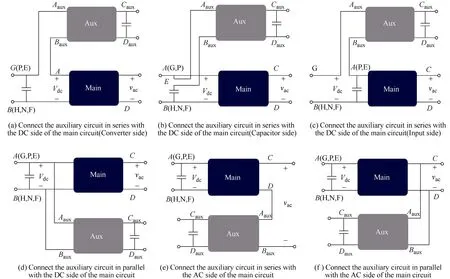
Fig.5 Typical structure diagrams of the active DC link (Aux) connected with the main circuit (Main)[25]
In principle, there are various choices of the passive elements and active circuit architectures for the active capacitor. A cost benchmarking of different active DC-link solutions for a 2.2kW single-phase inverter application is presented in [25, 42-43]. The capacitors,inductors, and semiconductor switches used in the inverter are sized with the same design margins and to system-level specifications (e.g., lifetime, output current total harmonic distortions). The results reveal that a few types of active DC links can achieve lower inverter design cost compared to a passive DC link in the scenario of a relatively high reliability requirement,which is relevant to many industry applications. In particular, solutions having a series-connected auxiliary circuit[45], and [46] are the most cost-effective ones. The methods presented in [45] and [46] enable lowest design cost since the auxiliary circuit processes the ripple voltage of the capacitor connected in series to it, and the ripple current of the DC link only. However, none of the active capacitive DC links can be used as a plugand-play active capacitor, since they have more terminals than a conventional capacitor, e.g., connections to an external power source for gate drivers and controller,and/or external feedback signals from the main circuits.
The circuit diagram of the two-terminal active capacitor is shown in Fig.6.vABandiABare the voltage and ripple current of the active capacitor, respectively. It consists of active switches, passive elements, a sampling and conditioning circuit, and self-powered controller and gate drivers. There are two power terminals A and B only, making it as convenient as a conventional passive capacitor from application point of view. As shown in Fig.6, the full-bridge circuit processes the ripple voltage and ripple current ofC1only, implying a lowVArating.A voltage control strategy is proposed based on internal voltage signalsvC1andvC2only, as shown in Fig.6,which does not require any current information from external circuits. Therefore, it enables fully independent operation of the active capacitor without any feedback signals from external circuits. The control objective is to shape the impedance seen fromABterminals to be that of an equivalent passive capacitor of interest. The experimental prototype of the two-terminal active capacitor is shown in Fig.7. Based on the specification of the case study, the impedance curves of the active capacitor and the comparable passive capacitor are shown in Fig.8. For a frequency at 120Hz or above, the impedance of the active capacitor is equivalent or lower than a passive capacitor with 34.4J rated energy storage.It implies that the active capacitor can achieve the same or even better harmonic filtering with 16.9% energy storage compared to a passive capacitor.
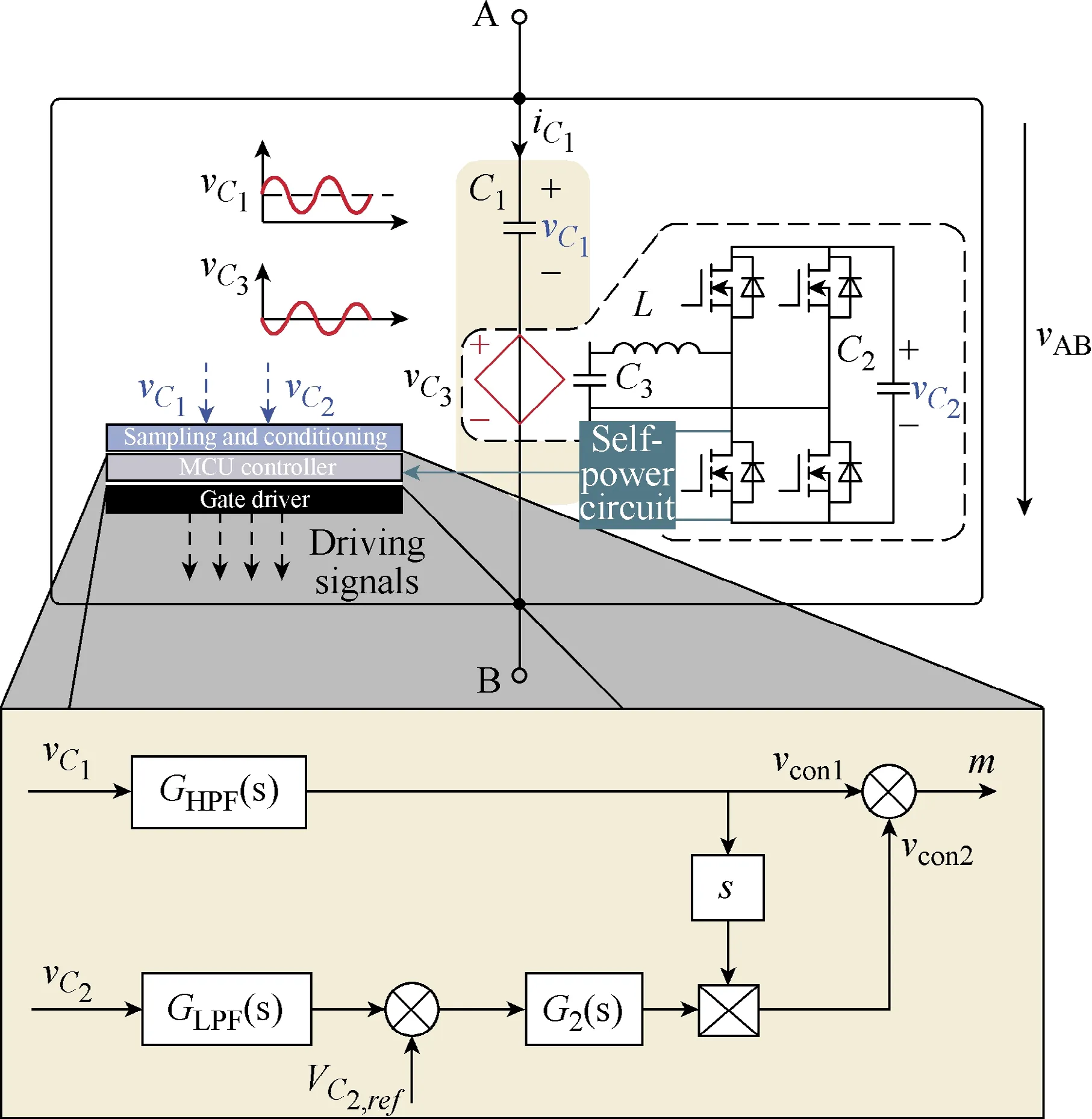
Fig.6 An implementation of the two-terminal active capacitor with a voltage control strategy[23] (vc1, vc2 and vc3 are capacitor voltages. GHPF(s) and GLPF(s) is the high pass filter(HPF) and low pass filter(LPF), respectively.G2(s) is the voltage controller for stabilizing vc2)
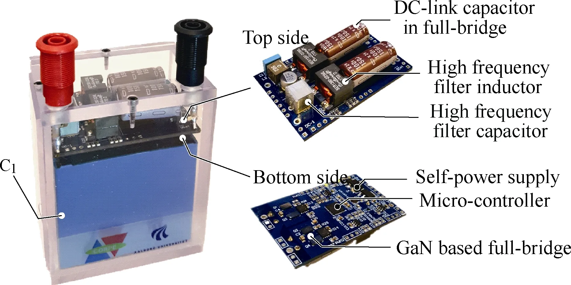
Fig.7 Prototype of the two-terminal active capacitor
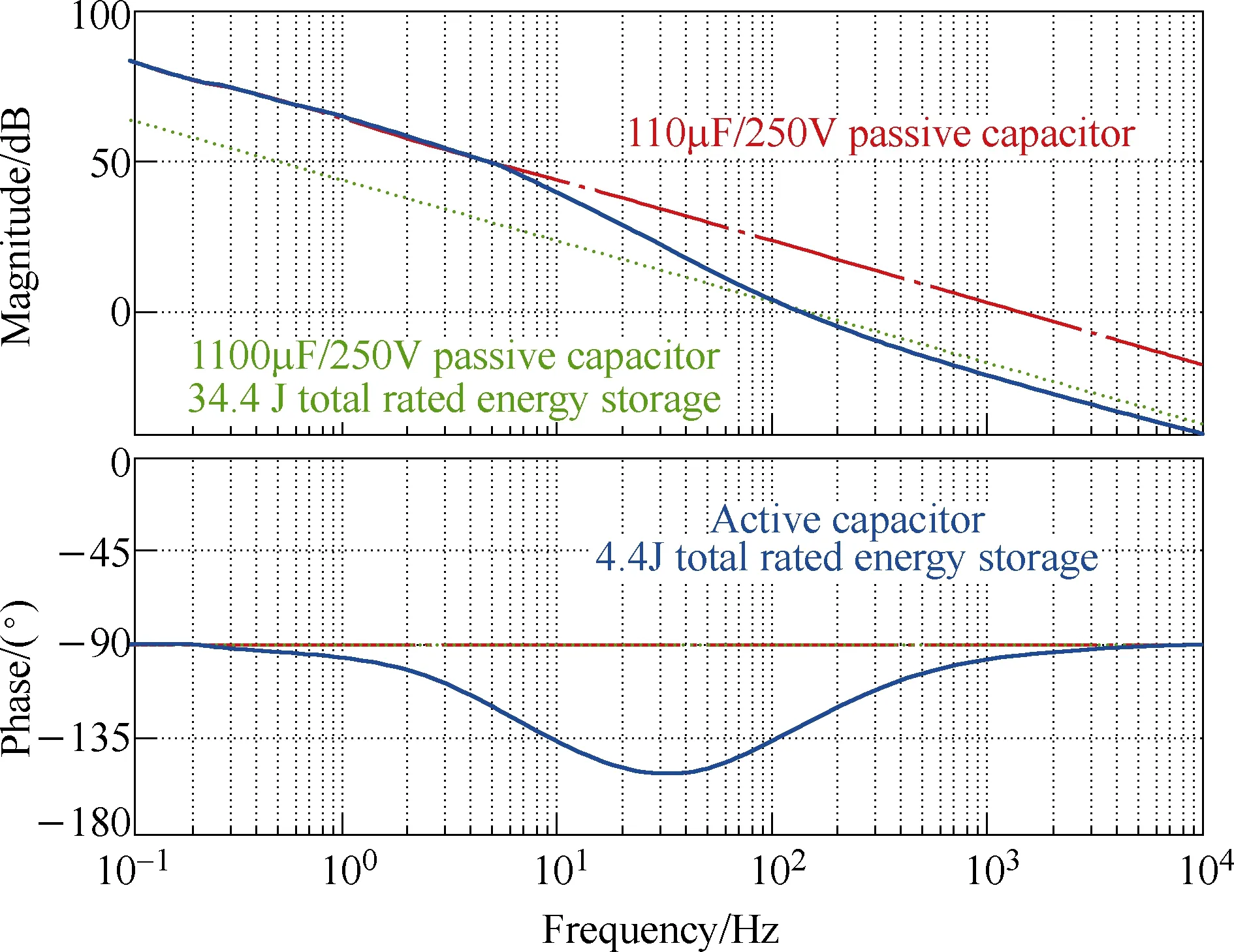
Fig.8 Bode diagram of the impedance of the active capacitor in the DC-link application[23]
5 Conclusions
The scientific challenges and existing studies on capacitive DC links are discussed in this paper.Among others things, the reliability aspect is especially addressed. Electro-thermal and lifetime modeling of capacitors to support model-based sizing and optimization of capacitor banks are presented. Two ways for useful lifetime matching of individual capacitors in a bank are briefly introduced with a case study. Besides passive solutions, the concepts and corresponding implementations of active capacitors are reviewed. A DC link with a two-terminal active capacitor is demonstrated by a case study, which represents the state-of-the-art active capacitive DC link solutions. From the authors’perspective, further research is needed to address the following scientific challenges in the topic discussed in this paper:
(1) Better mission profile data is needed to have better analysis of the actual stress levels of capacitors in power electronic applications. While extensive research has been done on the modeling of ripple current stress and internal temperature rise of capacitors, little study has been done on the modeling of the capacitor ambient temperature, which is affected by the heat dissipation of adjacent components, cooling system, and enclosure design, besides the environmental conditions. The capacitor bank thermal modeling discussed in this paper is an example of this effort. System-level thermal modeling and long-term mission profile data are essential to the capacitor ambient temperature profile analysis.
(2) These is still a lack of study on the impact of humidity and mechanical stresses on the wear out of capacitors, and on the catastrophic failure of capacitors due to single-event extreme stress. Besides the thermalrelated failure mechanisms presented in this paper, an understanding of the above failure mechanism will help to have a more comprehensive reliability analysis of capacitors.
(3) Solid proof of the reliability performance of active capacitive DC links is absent in literature, even though theoretical analysis shows the potential benefits.The two-terminal active capacitor concept enables not only the same level of convenience in use as passive capacitors, but also can be used to perform the accelerated degradation testing, which provides an opportunity for an experimentally comparative study on the reliability performance of active DC links and passive DC links.
 Chinese Journal of Electrical Engineering2018年3期
- Chinese Journal of Electrical Engineering的其它文章
- Prognostic Condition Monitoring for Wind Turbine Drivetrains via Generator Current Analysis
- A Review of Data-Driven Prognostic for IGBT Remaining Useful Life
- Thorough Validation of a Rotor Fault Diagnosis Methodology in Laboratory and Field Soft-Started Induction Motors
- Design, Implementation and Performance of Synchronous Current Regulators for AC Drives
- Circuit Implementation of Power Converter for High-Speed Switching Operations
- Study of the Characteristics and Suppression of EMI of Inverter with SiC and Si Devices
