Effect of ITIC and PVK Co-doped PCBM on The Performance of Perovskite Solar Cells
2018-08-28 08:47:02LIUShaoweiMIAOYaLIZhichengWANGYalingQINWenjingCAOHuanqiYANGLiyingYINShougen
发光学报 2018年8期
LIU Shao-wei,MIAO Ya,LI Zhi-cheng,WANG Ya-ling,QIN Wen-jing,CAO Huan-qi,YANG Li-ying* ,YIN Shou-gen*
(1.Key Laboratory of Display Materials and Photoelectric Devices,Education Ministry of China,School of Materials Science and Engineering,Tianjin University of Technology,Tianjin 300384,China;2.Tianjin Key Laboratory for Photoelectric Materials and Devices,Tianjin University of Technology,Tianjin 300384,China)
*Corresponding Authors,E-mail:liyingyang@tjut.edu.cn;sgyin@tjut.edu.cn
Abstract:In order to passivate the defects of the perovskite surface and improve the viscosity and film-forming properties of the PCBM solution so as to enhance the performance of device,the non-fullerene acceptor molecules(ITIC)and electron-rich poly(n-vinylcarbazole)(PVK)are used as additives of PCBM film.As a result,the interface morphology and the performance of PCBM are optimized by adjusting the content of ITIC and PVK.The optimal device is obtained when the ITIC content is 6%(mass fraction).Compared with the control device without additives,the power conversion efficiency(PCE)is increased from 5.26%to 9.93%,with no hysteresis.It is found that the introduction of ITIC and PVK improves the film-forming properties of PCBM.Moreover,the surface defect state of perovskite is passivated.The synergy is beneficial to the charge transport and separation.In summary,the addition of PVK and ITIC inhibits the moisture and oxygen in the atmosphere into the device and improves the stability of the device.
Key words:perovskite solar cells;interface engineering;hole-blocking;charge separation interfacial contact CLC number:TM914.4 Document code:A DOI:10.3788/fgxb20183908.1151
1 Introduction
In recent years,the power conversion efficiency of organic-inorganic hybrid perovskite solar devices has increased from 3.8%to 22.1%[1-3].Currently,most perovskite-based devices utilize a mesoporous metal-oxide(TiO2or Al2O3)to provide a porous substrate and also be responsible for accepting electrons.However,the mesoporous TiO2layer requires high sintering temperature,which increases the manufacturing cost and renders them incompatible with the flexible substrate[4].Therefore,the planar heterojunction perovskite solar cells have been paid much attention[5-6].However,the conventional planar structure devices often exhibit obvious hysteresis.The inverted planar structure exhibits lower hysteresis of J-V characteristics,due to the fact that fullerene derivative PCBM can effectively passivate the surface defects[7].PCBM has superior electron mobility and electron injection capability,which is used as electron transport layer(ETL)material in inverted planar structure devices.However,the low viscosity of the PCBM solution leads to poor filmforming property and poor interfacial contact with the electrodes.By adding polystyrene into the PCBM solutions,Bai et al.get a better coverage on the perovskite layer and effectively suppress the recombination of the photo-generated carrier[8].Zhu et al.found that the doped polymer semiconductor material PFNOX promotes the electron injection from perovskite to ETL and suppresses charge recombination[9].In our previous work,polyethyleneimine(PEI)with an alkylamine side chains that was used as an additive to modify the PCBM layer.It was found that PEI can promote the electron transfer between the perovskite layer and the cathode[10].The electron-rich polymer of polyvinylcarbazole(PVK)was also added into the PCBM layer to provide unshared pair electrons for Pb atom that form coordination or covalent bonds with the perovskite surface,passivating the perovskite surface defects and improving the viscosity and filmforming property of the PCBM solution.As a result,a more compact and dense PCBM film is obtained[11].
In this paper,the performance and stability of the device using the non-fullerene small molecule of 3,9-bis(2-methylene-(3-(1,1-dicyanomethylene)-indanone))-5,5,11,11-tetrakis(4-hexylphenyl)-dithieno[2,3-d:2',3'-d']-s-indaceno[1,2-b:5,6-b'] dithiophene)(ITIC)[12]and PVK co-doped PCBM as ETL layer is investigated.ITIC contains unshared pair electrons,which can passivate the surface defect states of perovskite.It is found that the introduction of ITIC and PVK improves the filmforming properties of PCBM.Moreover,the surface defect state of perovskite is passivated.The synergy is beneficial to the charge transport and separation.
2 Experiments
2.1 Experimental Materials
The molecular structure of the materials used in our experiment is in Fig.1.Fullerene derivatives(PCBM)(99%purity)are purchased from Solenne BV,the Netherlands.ITIC(purity of 99%)is obtained from Shanghai Vizu Chemical Company.PVK(Spectral Grade)is purchased from Aldrich Chemical Company.Lead iodide(PbI2,purity 99.995%)is purchased from Alfa Aesar.CH3NH3I(purity of 99.995%)is purchased from Kunshan Sunlite New Energy Technology Co.,Ltd.Isopropyl alcohol,odichlorobenzene,N,N-dimethylformamide(DMF)are 99.9%purity that are purchased from Beijing J&K Technology Co.,Ltd.
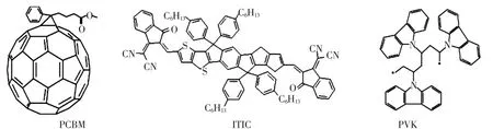
Fig.1 Molecular structure of PCBM,ITIC and PVK.
2.2 Device fabracation
PEDOT∶PSS aqueous solution is spin-coated on the ITO substrates(3 000 r/min,30 s),then the film is annealed(120℃,25 min).The PbI2DMF solution(0.5 mol/L)and ITO substrate are preheated(50 ℃,2 min)and 170 μL PbI2solutions are spin-coated(6 000 r/min,30 s)and annealed(70℃,10 min).The reaction is carried out using 120 μL of CH3NH3I(0.239 mol/L)in isopropyl alcohol solution and PbI2thin film(0 r/min,30 s,then 6 000 r/min,20 s),the perovskite film is annealed(60℃,10 min,then 100℃,20 min).Then ITIC and PVK co-doped PCBM o-dichlorobenzene solution(24 mg/mL)is spin-coated at a certain speed for 60 s.The final film is annealed at 100 ℃ for 10 min.Finally,Al cathode(120 nm)is deposited by thermal evaporation under vacuum of ~5 ×10⁻⁵Pa.The effective area of the device is 0.1 cm2.The device structure,energy level and section of SEM image are shown in Fig.2.
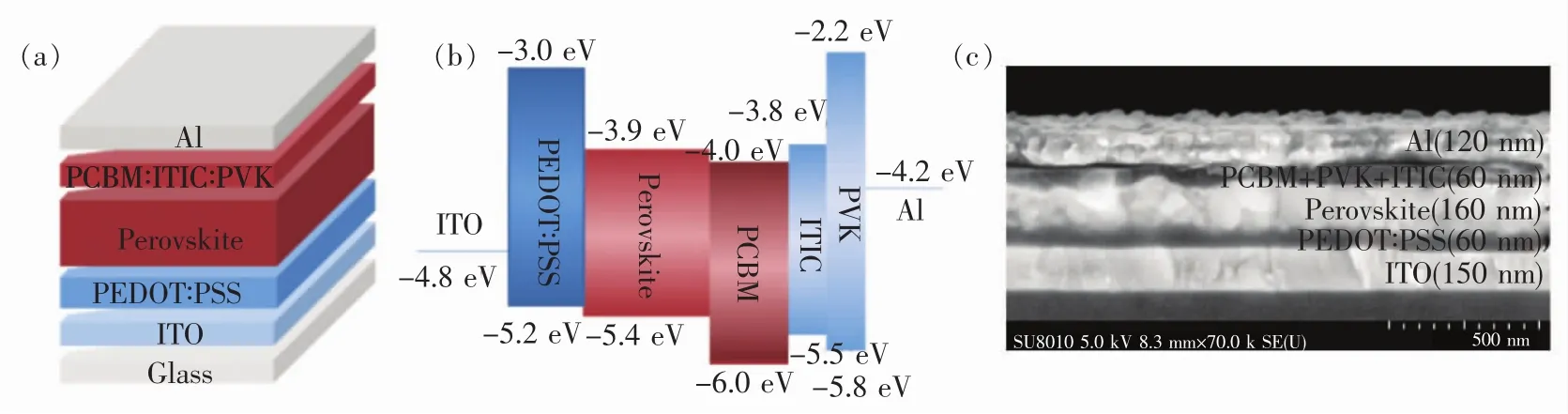
Fig.2 Device structure of the inverted planar heterojunction perovskite solar cell(a),schematic energy level diagram(b)and section of SEM images(c).
3 Results and Discussion
J-V characteristics of the device with different ITIC contents are shown in Fig.3.The device structure is ITO/PEDOT∶PSS/CH3NH3PbI3/PCBM+4%PVK+(0 - 8%)ITIC/Al.Tab.1 lists the detailed performance parameters of device(Jsc,Voc,FF and PCE).It can be seen from Fig.3 and Tab.1 that the optimal performance is obtained at the contents of ITIC is 6%(mass fraction).Compared with the control device containing pure PCBM as ETL,the Vocis increased from 0.86 to 0.95 V.Jscis increased from 13.02 to 15.97 mA/cm2.FF is increased from 40.90%to 65.42%,and the power conversion efficiency is increased from 5.26% to 9.93%.The enhancement of Voccan be attributed to the improvement of the interface contact in the device,the effective separation of photo-generated charge and the energy level matching.The increased Jscis resulted from the good film forming characteristics of PCBM film doped with ITIC and PVK.Fig.4 shows J-V characteristics of the optimal device for PCBM+4%PVK+6%ITIC as ETL.It can be seen that the forward and reverse curve is almost identical with no obvious hysteresis.This means that by adding PVK and ITIC into PCBM can not only reduce the defects state of perovskite surface,but also make good interface contactbetween perovskite layer and Al electrode[13-14].The dark J-V characteristic curves of devices with PVK and ITIC co-doped PCBM show obviously lower reversed saturation current and higher rectification ratio compared to that based on pure PCBM.
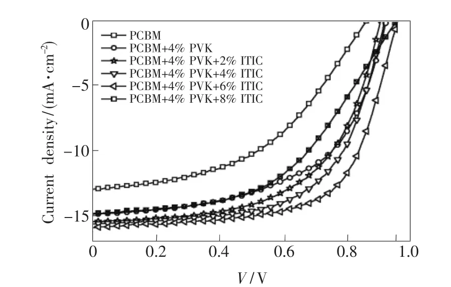
Fig.3 J-V characteristics of the device with different ITIC mass fraction
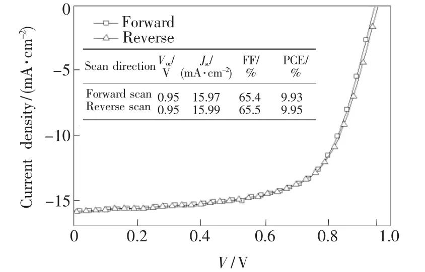
Fig.4 J-V characteristics for the optimal device measured with the bias scanned in different directions

Tab.1 Summary of device performances for the perovskite solar cells with different condition
Fig.5 is the AFM height images of the PCBM samples with different ITIC mass fraction added to PCBM+4%PVK solutions.The root meant-squared roughness(Rq)and average roughness(Ra)of pristine PCBM layers are 1.88 nm and 1.40 nm,respectively.The surface smoothness of the PCBM film improved with the contents of ITIC is further increased.Rqand Ravalues are decreased to 1.45 nm and 1.05 nm respectively when the optimal mass fraction of ITIC is 6%.We may reasonably conclude that the addition of ITIC and PVK to the PCBM solution makes the ETL more dense and smooth.ITIC is an amorphous organic molecule with weak crystallization[15].As a result,ITIC can contact with the rigid domains of PCBM closely.

Fig.5 AFM height images of PCBM samples with different ITIC mass fraction(a:0%;b:2%;c:4%;d:6%;e:8%)
Surface photovoltage spectroscopy(SPS)is used to determine the intensity of the response of the surface to light.Surface photovoltage is produced by the separation of photo-generated electron and hole in the device[16].A stronger response of SPV indicates that photo-generated charges can be separated and transported efficiently.Fig.6 shows the response of SPV in the 400-1 000 nm spectral region of a sample with the configuration of ITO/PEDOT∶PSS/CH3NH3PbI3/PCBM+4%PVK+(0-8%)ITIC.We can see that the SPV response of the samples without ITIC is weak.When ITIC is added,we can observe that the SPV response is enhanced significantly and the spectral response range appears broad and strong.The above results show that the PVK+ITIC co-doped PCBM samples show high light sensitivity.This means that the addition of ITIC increases the efficiency of charge-transfer separation.Moreover,the ITIC can passivate the surface trap states of perovskite,thereby reducing recombination of the charge at the interface between the perovskite and the PCBM,which brings the significant improvement in FF and Jscas well as the whole device efficiency[17].
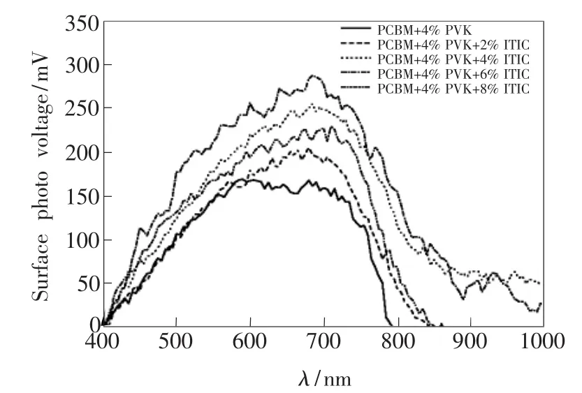
Fig.6 SPS measurements of the samples with different ITIC mass fration
Fig.7(a)shows the UV-Vis absorption spectra of ITIC(40 nm),PCBM(40 nm),CH3NH3PbI3and CH3NH3PbI3/PCBM+4%PVK+6%ITIC thin films.The absorption of the layer of CH3NH3PbI3is enhanced at 330-400 nm for PCBM film containing 4%PVK+6%ITIC.Both the PCBM film with different concentration of ITIC and pure PCBM film have no obvious change in absorption.The performance enhancement of ITIC and PVK co-doped PCBM device is not resulting from enhanced absorption.The PL measurements of the perovskite/PCBM films without and with 4%PVK+6%ITIC are shown in Fig.7(b).It can be observed that the PL intensity of perovskite/PCBM+4%PVK+6%ITIC is significantly lower than perovskite/PCBM.Besides,the PL peak of pure PCBM is at 749 nm.However,the PL peak of PVK+ITIC co-doped PCBM is at 719 nm,a blue shift of about 30 nm is occurred.Both of these phenomenon revealed that PVK+ITIC co-doped PCBM reduces perovskite surface defects.

Fig.7 UV-Vis absorption spectrum of ITIC,PCBM,CH3-NH3PbI3and PCBM+4%PVK+6%ITIC(a)and PL spectra of perovskite/PCBM and perovskite/PCBM+4%PVK+6%ITIC films(excited by a 360 nm light source)(b).
Fig.8 shows the relationship between the normalized efficiency and the storage time of the device(8 cells for each device structure).Degradation speed of devices based on pure PCBM is faster than devices based on PVK and ITIC co-doped PCBM significantly.It can be found that the improved stability of the device is obtained for the device with 4%PVK and 6%ITIC co-doped PCBM.The PCE is only decayed to 71%of the original value after 8 d.This indicates that PVK and ITIC co-doped PCBM can prevent moisture and oxygen on the PCBM layer from the environment,thereby enhancing the stability of the device.

Fig.8 Normalized degradation characteristics of device performance within 8 d
4 Conclusion
The inverted planar PSCs were fabricated using non-fullerene acceptor small molecules(ITIC)and electron-rich poly(PVK)as additives of PCBM film.The results show that the interface morphology can be optimized and the performance of the device can be improved by adjusting the concentration of ITIC.The optimal device performance is obtained at the concentration of ITIC was 6%(mass fraction).It is found thatthe introduction ofITIC and PVK improves thefilm-forming propertiesofPCBM.Moreover,the surface defect state of perovskite is passivated.The synergy is beneficial to the charge transport and separation.In summary,addition of PVK and ITIC inhibits the moisture and oxygen in the atmosphere into the device and improves the stability of the device.