
Definition and application of easily measurable aspheric surfaces
2017-04-10 03:34YOUSSEFAlKhatibMOHAMEDFawazMoussellyMAMOUNNaim
中国光学 2017年2期
YOUSSEF Al-Khatib, MOHAMED Fawaz Mousselly, MAMOUN Naim
(HigherInstituteforAppliedSciencesandTechnologyDamascus,Damascus,Syria)
Definition and application of easily measurable aspheric surfaces
YOUSSEF Al-Khatib, MOHAMED Fawaz Mousselly*, MAMOUN Naim
(HigherInstituteforAppliedSciencesandTechnologyDamascus,Damascus,Syria)
This paper presents a new kind of “Easily Measurable Aspheric Surfaces”(EMAS), which could be easily measured by a traditional optical interferometer. The measurement of EMAS is mainly based on using the multi-configuration feature in Zemax software. The first configuration represents the optical system with EMAS, and the second configuration represents the setup, using a parallel planes glass plate or a single lens as a null corrector to measure the aspheric surface used in the first configuration. The applications and advantages of this technique are illustrated by many examples, which could confirm the ease of manipulating and testing this kind of surfaces, compared with conical or general aspheric surfaces. It can also show its competence in minimizing the optical aberrations.
easily measurable aspheric surfaces;interferometer;null test
1 Introduction
In the 15th century, scientists succeeded in designing the first optical systems using lenses or mirrors with spherical surfaces. Since the spherical surface has a constant curvature at all its points, it was possible to control the surfaces while manufacturing. Such systems were satisfactory at that time, but the rapid development in technical fields lead to the need for optical systems with better performance while being compact. Therefore, aspheric surfaces, though being difficult to manufacture and test, were the only option for optical designers when compactness or highest optical performance were required[1-2].
The accurate metrology of optical surfaces is usually achieved by means of optical interferometers[3-4]. In such systems, the emitted spherical wave-front has to be diffraction-limit with radius of curvature matching that of the surface under test, so the optical rays fall perpendicularly upon the tested surface. Then, the reflected rays will be precisely coincident with the incident rays, which could make this method very sensitive to any sub-micron deviation over the whole of the tested surface[5-6].
On the other hand, general aspheric surfaces cannot be directly measured using standard interferometers, and a suitable null corrector has to be introduced between the interferometer and the aspheric surface[7]. The null corrector function is to convert a spherical or plane wave-front into a form which could match the profile of the aspheric surface under test. As a result, the interferogram will display straight, parallel, and equally spaced fringes if the aspheric surface under test has the profile requested in the lens drawing. A variety of designs of null correctors are presented in several articles related in optics, and each corrector has been designed and manufactured to measure a specific aspheric surfaces[7].
The design and handling of a null corrector are usually difficult because it is made of several lenses which have to be perfectly manufactured, and then accurately assembled. Even if the null corrector has been produced within the acceptable tolerances, the accuracy of the measurement requires the corrector to be precisely placed, relative to the aspheric surface and the interferometer. In this context it is appropriate to recall the problem of the Hubble Space Telescope where an incorrectly placed null lens resulted in the primary mirror being ground to an inaccurate surface figure, and thus producing strong spherical aberrations[8].
The main goal of this study is to put forward a new technique where the optical design uses Easily Measurable Aspheric Surfaces(EMAS) instead of general aspheric surfaces, and this technique overpowers the problematic measurement of general aspheric surfaces. Thus, the outcome of this research is to provide the optical designer with a methodology allowing simultaneously the effective use of aspheric surfaces to achieve higher performances and a reduction of optical system size, while being able to easily measure such aspheric surfaces with the devices available in all optical workshops, transforming the well-known sentence “You can't manufacture what you can′t measure” to “Why don't you design what you can easily measure”.
2 Definition of EMAS
Aspheric surfaces are described by a polynomial expansion of the departure from a spherical surface. The even aspheric surface model uses only the even powers of the radial coordinate. The surface sag is given by equation (1)[9]:
SAGevensphere(C0,k,r)=
WhereC0is the curvature at the vertex;kis the conic constant. The first term in the previous equation describes the surface sag for a conical surface.
As described in the introduction, general aspheric surfaces could probably be tested using null correctors consisting of several optical elements. For example, Fig.1 shows Shafer null corrector consisting of 3 lenses[10], while Fig.2 shows an Offner null corrector comprising two lenses[10]. In Fig.2, the first lens is called the field lens and its function is to image the aspheric surface onto the second lens which is called the relay lens. The role of the relay lens is to produce spherical aberration equaling the difference between the aspheric surface and the best-fit spherical surface[11-13].
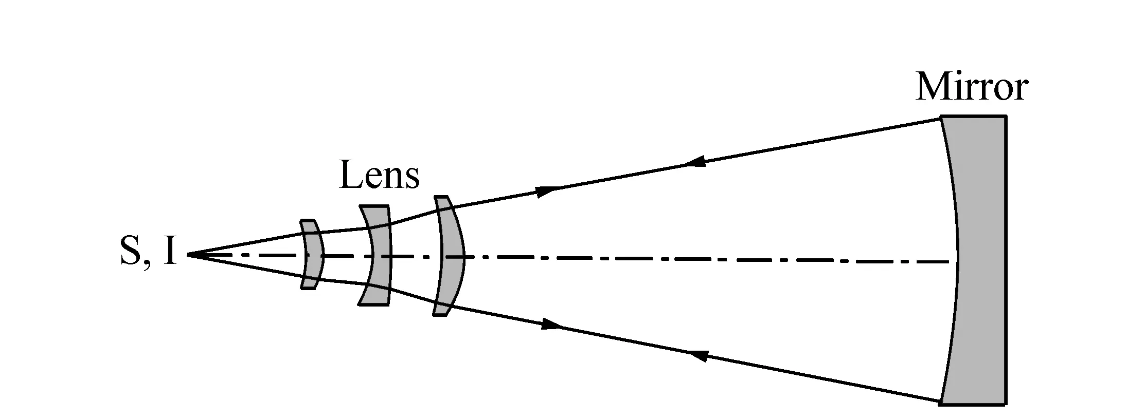
Fig.1 Schematics of Shafer null corrector[10]
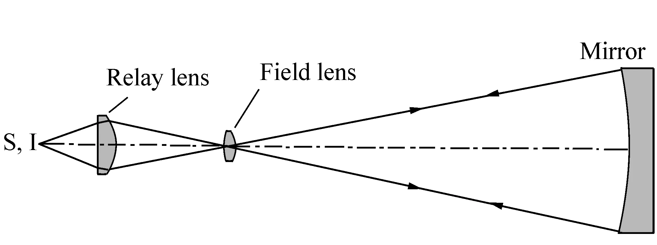
Fig.2 Schematics of Offner null corrector[10]
EMAS are defined in this paper as the aspheric surfaces that can be tested by an optical interferometer using only one optical element as a null corrector in one of two cases:the first case includes the use of a parallel planes glass plate with a spherical wave-front(see Fig.3), and the second case uses one lens with a plane wave-front(see Fig.4). The two simple null correctors are easy to manufacture and less sensitive to their relative place between the aspheric surface and the interferometer.
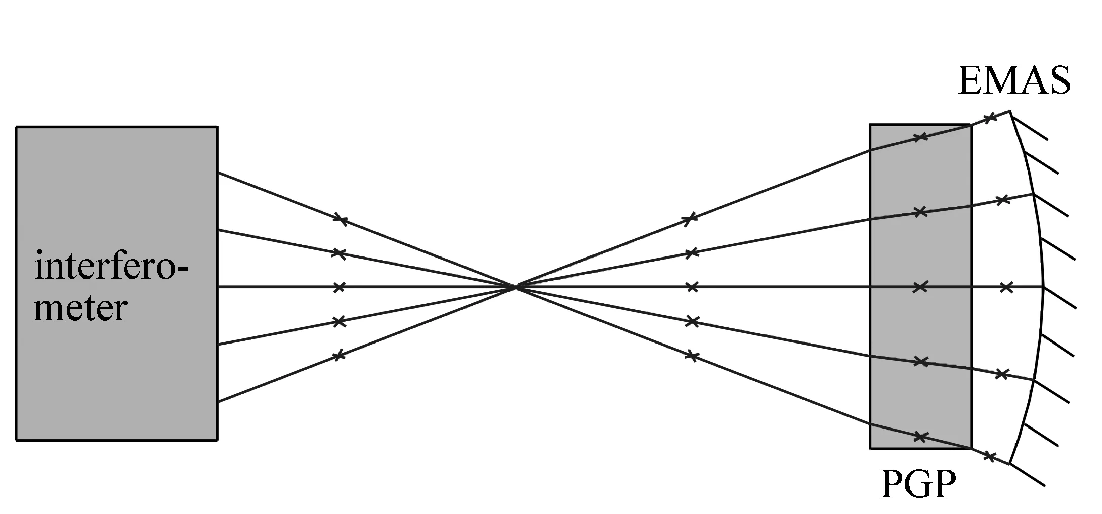
Fig.3 Testing EMAS by a parallel planes glass plate as null corrector with aspherical wave-front

Fig.4 Testing EMAS by a single lens as null corrector with a plan wave-front
3 Design technique using EMAS
The aim of using EMAS is two-folds including minimization of the optical aberrations and using aspheric surfaces that can be easily measured. Therefore, two different optical systems have to be designed. The first system represents the required optical system with as minimal aberrations as possible using an aspheric surface, and the second optical system represents one of the null test setups illustrated in Fig.3 and Fig.4 is used to measure the aspheric surface appearing in the first optical system.
To satisfy simultaneously these two conditions, a “multi-configuration” feature in optical design software “Zemax” has to be applied. The first configuration consists of the required optical system with suitable operands to satisfy the wanted optical system constrains, e.g. field of view, wavelengths, total track, image quality,etal. One of the surfaces in this configuration is chosen to be aspheric, or more specifically this surface would be EMAS. The second configuration is built with operands which could be suitable to the measurement setup constrains, e.g. field of view is zero, monochromatic wave length(He-Ne), double pass mode,etal, in addition to the parameters of the mirror surface which are “picked up” from the parameters of EMAS defined in the first configuration.
The following paragraphs present three different examples, demonstrating the usefulness and easiness of the proposed technique.
3.1 Designing an objective lens made of Germanium
In this example, an objective lens for a thermal camera has been designed with the following parameters:
•Field of view:±6.5 degrees
•Main wavelengths:8, 10, 12 μm
•Effective focal length:55 mm
•Total track:less than 80 mm
•F/# :1.2
Two Germanium lenses have been used in the design. The first surface of the first lens is selected to be even-aspheric, and would become EMAS.
The null test setup to measure this EMAS is chosen as in Fig.3(i.e. parallel planes glass plate with spherical wave-front) but in this case the tested surface is convex; and the test wave length is 0.632 8 μm.
Two configurations have been created in Zemax software. The first configuration represents the design of the objective lens, and the second one represents the null test setup.The parameters of EMAS in the second configuration have been picked up from the first configuration. The suitable start values of other parameters(curvatures, thickness,etal) have been selected carefully to satisfy the design requirements(see Tab.1).

Tab.1 Parameters of the two configurations:Config 1 for the objective lens; Config 2 for the test setup
Then, a default merit function has been generated, and the total track and effective focal length have been inserted for the first configuration(the manual of each optical design software gives full details of multi-configuration operands[14]). Afterwards, through repeated optimization, we obtained the final design of the objective lens as listed in Tab.2.
Tab.2 Final lens objective design in Zemax software
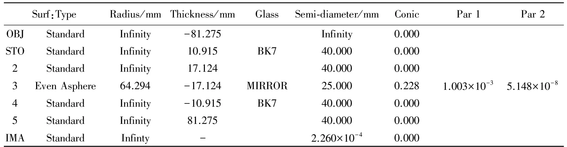
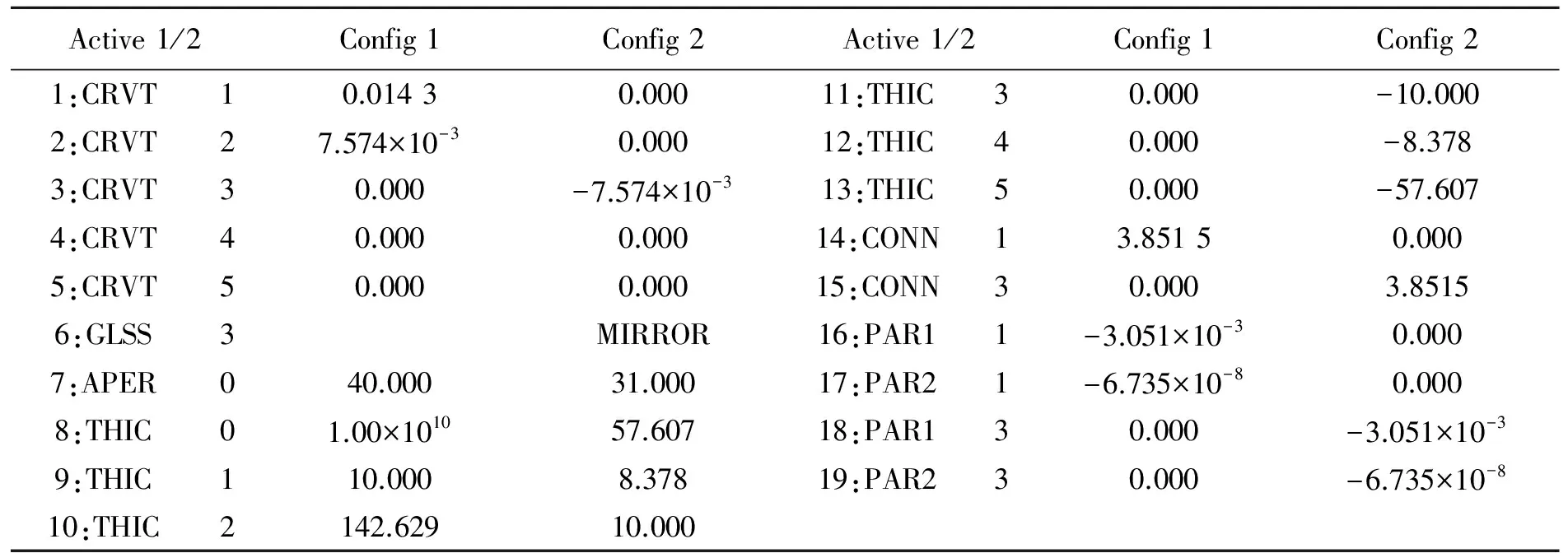
Fig.5 shows the objective lens and the modulating transfer function MTF, and the MTF chart demonstrates that this design is nearly diffraction-limit.

Fig.6 MTF chart of an optimized objective lens with conical surface instead of EMAS
For the completeness of the discussion, Fig.6 shows the resulted MTF when a conical surface has been used and optimized, instead of using EMAS. It is clear that the performance of the objective lens with EMAS is better than that with the conical surface at the field of 6.5°. This result can be justified by the fact that although there are special constraints imposed on EMAS for being in the second configuration, it has more variables that could be altered during the optimization than the conical surface.
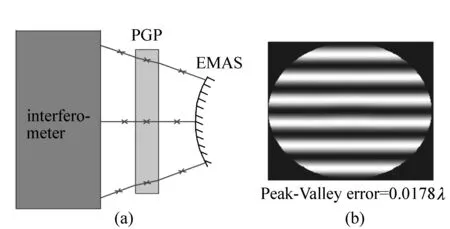
Fig.7 (a)Null test layout, (b)resulted interferogram of the EMAS
The null test setup to measure the obtained EMAS using a parallel planes glass plate as a null lens is illustrated in Tab.3. The layout and the resulted interferogram are shown in Fig.7. It is worth mentioning that the surface 1(stop, even-aspher surface) in Tab.2 has the same parameters as the surface 3(surface under test) in Tab.3.
Tab.3 Final null test of the EMAS used in the objective lens design
The straight and equidistant lines in the interferogram with Peak to Valley error of less thanλ/50 could confirm that the parallel planes glass plate acts like a good null lens in this case. Another article by the same authors demonstrates that the use of parallel planes glass plate as a null corrector is much easier than designing and using conventional null lens[?].
3.2 Designing an objective lens of Germanium using a null corrector containing only one lens
In some cases, it is not possible to get a good optical performance design using EMAS with a null test setup of the first type(see Fig.3). Therefore, this example shows an objective lens which has the same parameters as in the previous example, but the null test setup is of the second type(see Fig.4). A suitable multi-configuration has been created in Zemax software to achieve the desired requirements(see Tab.4). A successive optimization has been applied. In this case the second surface of the first lens has been selected as EMAS. Note that the curvature of the tested surface in the second configuration picked up with it by factor-1(operands 2 and 3).

Tab.4 Parameters of the two configurations:Config 1 for the objective lens; Config 2 for the test setup
The final design of the objective lens is shown in Tab.5, while Fig.8 shows the design layout and the MTF chart.
Comparing MTF curves in Fig.5 and Fig.8, it is clear that the same results are obtained in both cases.

Tab.5 Final lens objective design in Zemax software
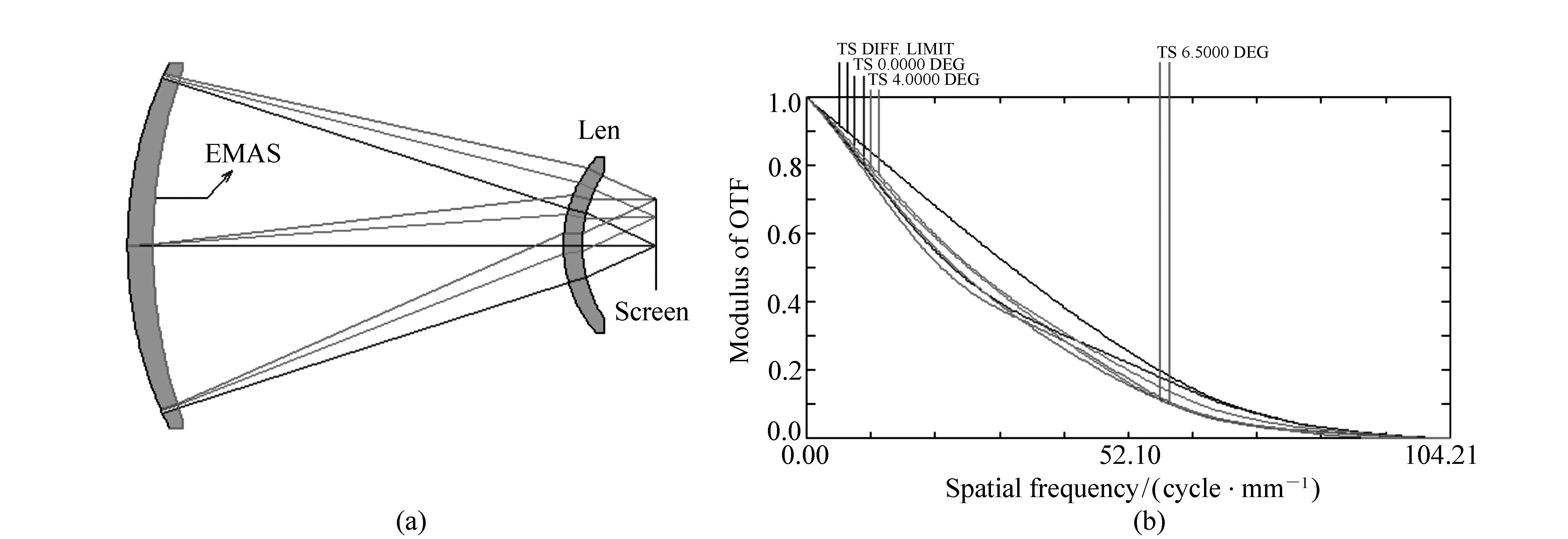
Fig.8 (a)Final lens objective layout, (b)resulted MTF curves

Surf:TypeRadius/mmThickness/mmGlassSemi⁃diameter/mmConicPar1Par2Par3OBJStandardInfinityInfinity00.000STOStandard-33.41810.000BK718.0000.0002Standard-514.86520.00020.0000.0003EvenAsphere-83.516-20.000MIRROR25.0000.7418.314×10-4-7.988×10-93.421×10-124Standard-514.865-10.000BK720.0000.0005Standard-33.418-15.00018.0000.0006Paraxial-20.00016.66620.00000IMAStandardInfinity-1.24×10-40.000
Tab.6 shows the null test setup parameters to measure the EMAS, while Fig.9 shows the null test layout and the resulted interferogram. The Peak to Valley error in this case is less thanλ/150.
Fig.9 (a)Null test layout, (b)resulted interferogram of the final EMAS
Single null lens is more difficult to use than the plane parallel glass plate that was used in the previews example, but its use is definitely easier than
conventional null lens(like Offner or Shafer null lens), because the relative position of the single null lens to the interferometer is not critical, since the incident beam is plan.
3.3 Example of using EMAS in a laser collimating lens
This example uses EMAS to design a laser collimating lens with a concave surface. The collimating lens has the following parameters:
•Effective focal length:150 mm
•Working wave length:0.632 8 μm(HeNe)
•Clear aperture:20 mm
The two configurations have been built as described before(see Tab.7), and the Null test setup has been chosen of the first type(see Fig.3). Tab.8 shows the final lens design, while Fig.10 shows the layout and the MTF chart.
Tab.7 Two configurations table, Config 1 for the collimating lens; Config 2 for the null test

Tab.8 Final collimating lens design in Zemax software
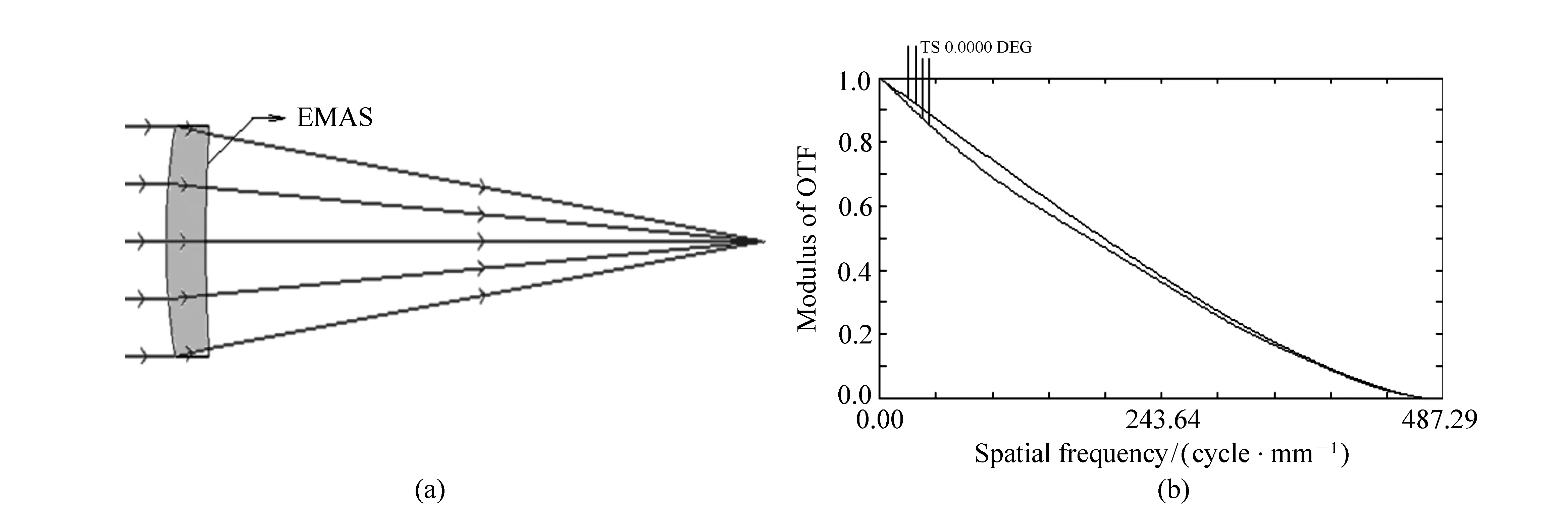
Fig.10 (a)Collimating lens layout, (b)resulted MTF curves
Tab.9 shows the null test setup design, and the layout and the resulted interferogram are shown in Fig.11. The Peak to Valley error is less thanλ/10.

Tab.9 Final Null test of the EMAS used in the collimating lens design
Fig.11 (a)Null test layout, (b)resulted interferogram of the final EMAS
4 Advantages of using EMAS
The use of EMAS is highly beneficial because it does not require any expensive and specialized instruments that are not normally available in optical workshops. Actually, a typical null lens used in metrology usually consists of more than one optical element, and in some cases it may contain diffractive elements. In addition, the following notes have to be taken in consideration when designing, manufacturing, and assembling any conventional null corrector.
(1)Optical elements must be fabricated, and null lens must be assembled, with extremely high accuracy, because they are made to measure aspheric surfaces.
(2)The placement of the null lens must be defined and maintained accurately, referring to Hubble Space Telescope primary mirror problem[8].
(3)The optical axis of the interferometer and the null lens must be accurately coincident. This step is usually achieved using expensive auxiliary elements, and needs a lot of expertise and time.
On the other hand, EMAS allows the use of a plane parallel glass plate as null lens(spherical wave-front) or a null lens compromising only one lens(plane wave-front). Those simple null lenses have the following advantages:
(4)Plane parallel glass plate is easy to fabricate since it is a plate of glass with only two parallel surfaces.
(5)Plane parallel glass plate has not a specific optical axis, so it can be shifted up and down, right and left without effecting the accuracy of the measurement.
(6)Plane parallel glass plate has no optical power, so its use is not sensitive to its position between the interferometer and the aspheric surface under test.
(7)Only one lens with plane incident wave-front is easier to be aligned with the interferometer than Offner or Shafer null lenses.
It also important to stress on the fact that an EMAS surface has more variables to change(more degrees of freedom) than aconical surface, so it may lead to better performance of the optical system when compared to a conical surface.
5 Conclusion
This paper proposes a new technique for aspheric optical design. The technique defines “Easily Measurable Aspheric Surfaces”(EMAS). The paper shows that EMAS can effectively minimize optical aberrations because of its asphericity, while being much easier to be tested compared to the general aspheric surfaces. Many examples have been presented to demonstrate the advantages of EMAS, and to show how it can be applied in optical design. The obtained results will hopefully encourage optical designers to use this kind of surfaces instead of conical or general aspheric surfaces which would require expansive and specialized devices and accessories.
[1] SCHULZ,GÜNTER. Imaging performance of aspherics in comparison with spherical surfaces[J].AppliedOptics,1987,26(23):5118-5124.
[2] BRAUNECKER B,HENTSCHEL R,TIZIANI H.AdvancedOpticsUsingAsphericalElements[M]. Bellingham,USA:SPIE,2008.
[3] BRIERS J. DAVID. Optical testing:a review and tutorial for optical engineers[J].OpticsandLasersinEngineering,1999,32:111-138.
[4] SHI T U,ET A L. Surface testing methods of aspheric optical elements[J] .ChineseOptics,2014,7(1):26-46.
[5] MALACARA,DANIEL.OpticalShopTesting[M]. New Jersey:John Wiley & Sons,2007.
[6] WANG X K. Compensation of misalignment error on testing aspheric surface by subaperture stitching interferometry[J].ChineseOptics,2013,6(1):88-95.
[7] OFFNER,ABE. A null corrector for paraboloidal mirrors[J].AppliedOptics,1963,2(2):153-155.
[8] BOTTEMA,MURK. Reflective correctors for the Hubble Space Telescope axial instruments[J].AppliedOptics,1993,32(10):1768-1774.
[9] OKA,KEITA,SCOTT SPARROLD. Asphere Design for Dummies[J].SPIE,2012,8487:84870B.
[10] BURGE,JAMES HOWARD. Advanced techniques for measuring primary mirrors for astronomical telescopes[D]. Arizona:University of Arizona,1993.
[11] DEVOE,CATHERINE ELLEN. Limitations on aspheric surface testing with simple null correctors[D]. Arizona:Optical Sciences Center,University of Arizona Tucson,1989.
[12] SASIAN J M. Optimum configuration of the offner null corrector. testing an F#/1 paraboloid[J].SPIE,1989,1164:8-17.
[13] MALACARA-HERN NDEZ,DANIEL,ZACAR AS MALACARA-ERN NDEZ.HandbookofOpticalDesign[M]. Florida:CRC Press,2016.
[14] Zemax Manual:Optical Design Program User′s Guide[R]. Zemax,2009.
Author biographies:

YOUSSEF Al-Khateb(1976—), Master degree. His research interests are on optical design and optical metrology. E-mail:khatyos@hotmail.com

MOHAMED Fawaz Mousselly(1949—), Engineer Doctor, Professor. His research interest is optical and electro-optical systems development. E-mail:fawaz.mousselly@hiast.edu.sy
向您推荐《液晶与显示》期刊
● 中文核心期刊
● 中国液晶学科和显示技术领域的综合性专业学术期刊
● 中国物理学会液晶分会会刊、中国光学光电子行业协会液晶分会会刊
● 英国《科学文摘》(INSPEC)、美国《化学文摘》(CA)、俄罗斯《文摘杂志》(AJ)、美国《剑桥科学文摘》(CSA)、“中国科技论文统计源期刊”等20余种国内外著名检索刊物和文献数据库来源期刊
《液晶与显示》以材料物理和化学、器件制备技术及器件物理、器件驱动与控制、成像技术与图像处理等栏目集中报道国内外液晶学科和显示技术领域中最新理论研究、科研成果和创新技术,及时反映国内外本学科领域及产业信息动态,是宣传、展示我国该学科领域和产业科技创新实力与硕果,进行国际交流的平台。其内容丰富,涵盖面广,信息量大,可读性强,是我国专业学术期刊发行量最大的刊物之一。
《液晶与显示》征集有关液晶聚合物、胶体等软物质材料和各类显示材料及制备方法、液晶物理、液晶非线性光学、生物液晶;液晶显示、等离子体显示、发光二极管显示、电致发光显示、场发射显示、3D显示、微显示、真空荧光显示、电致变色显示及其他新型显示等各类显示器件物理和制作技术;各类显示新型模式和驱动技术、显示技术应用;显示材料和器件的测试方法与技术;各类显示器件的应用;与显示相关的成像技术与图像处理等研究论文。
《液晶与显示》热忱欢迎广大作者、读者广为利用,踊跃投稿和订阅。
地 址:长春市东南湖大路3888号 国内统一刊号:CN 22-1259/O4
《液晶与显示》 编辑部 国际标准刊号:ISSN 1007-2780
邮 编:130033 国内邮发代号:12-203
电 话:(0431)6176059 国内定价:50元/期
E-mail:yjyxs@126.com 网 址:www.yjyxs.com
2016-10-19;
2016-12-05
2095-1531(2017)02-0256-11
易测量非球面定义及应用
YOUSSEF Al-Khatib, MOHAMED Fawaz Mousselly*, MAMOUN Naim
(叙利亚应用科学与技术高等学校,大马士革 31983)
本文提出了一种新型、易于用传统光学干涉仪测量的非球面。该非球面的检测主要基于Zemax光学程序软件设计的多重配置特性。第一配置为易于测量非球面,第二配置为采用平行平面玻璃板或单透镜作为零位校正器,用于检测第一配置的非球面。本文通过一些实例,说明了易测量非球面检测技术的应用和优势,证实了与圆锥或普通非球面相比,易测量非球面更易于操作与检测,同时有利于减小光学像差。
易测量非球面;干涉仪;零位检验
TG806
A
10.3788/CO.20171002.0256
*Correspondingauthor,E-mail:fawaz.mousselly@hiast.edu.sy
猜你喜欢
光学仪器(2022年3期)2022-07-10
电子设计工程(2022年6期)2022-04-13
建材发展导向(2021年13期)2021-07-28
环境影响评价(2020年2期)2020-12-02
电子制作(2019年19期)2019-11-23
金刚石与磨料磨具工程(2019年4期)2019-09-19
电子制作(2017年13期)2017-12-15
航天制造技术(2016年6期)2016-05-09
数码世界(2009年2期)2009-09-02
祝您健康(1988年4期)1988-12-30
