结合椭圆偏振光谱与傅里叶红外光谱的宽禁带半导体薄膜光学特性表征
谢灯,丘志仁,万玲玉,TIN Chin-che,梅霆,冯哲川
(1.华南师范大学光电子材料与技术研究所,广州 510631;2.中山大学光电材料与技术国家重点实验室,物理学院,广州 510275;3.广西大学物理科学与工程技术学院,广西相对论天体物理重点实验室,光电子材料与探测技术实验室,南宁 530004;4.马来西亚大学机械工程系,马来西亚 吉隆坡 50603;5.奥本大学物理学院,美国 奥本36849;6.西北工业大学理学院,教育部空间应用物理与化学重点实验室,陕西省光信息技术重点实验室,西安710072)
结合椭圆偏振光谱与傅里叶红外光谱的宽禁带半导体薄膜光学特性表征
谢灯1,2,丘志仁2*,万玲玉3,TIN Chin-che4,5,梅霆6,冯哲川3
(1.华南师范大学光电子材料与技术研究所,广州 510631;2.中山大学光电材料与技术国家重点实验室,物理学院,广州 510275;3.广西大学物理科学与工程技术学院,广西相对论天体物理重点实验室,光电子材料与探测技术实验室,南宁 530004;4.马来西亚大学机械工程系,马来西亚 吉隆坡 50603;5.奥本大学物理学院,美国 奥本36849;6.西北工业大学理学院,教育部空间应用物理与化学重点实验室,陕西省光信息技术重点实验室,西安710072)
宽禁带半导体薄膜,包括碳化硅,氮化镓和氧化锌及其化合物以及异构体,带隙普遍在3.2 eV以上,一阶声子特征峰在100至1500 cm-1之间。确定能带宽度和声子特征峰有很多方法,比如光致发光、拉曼散射、光学透射谱等,我们提出了一种结合椭圆偏振光谱与红外傅里叶反射谱进行传输矩阵分析的方法,能够同时确定从紫外波段(约250 nm)到远红外波段(约22000 nm)的薄膜材料色散关系和膜厚。我们构建了基于谐振子的光学函数模型,并论证这个模型很适合用于模拟由各种不同波长入射光波造成的共振吸收。
椭圆偏振光谱;傅里叶红外光谱;传输矩阵方法
1 Introduction
In the past decades,wide bandgap semiconductors attracted much attention due to their significant advantages in ultra-violet optoelectronic applications.GaN,SiC and ZnO-based materials have their niche areas of applications,respectively.For example,GaN and related ternary- quaternary- components are easier to implement bandgap engineering,hence suitable as the active region of light emiting diode by growing multiple quantum wells on sapphire or silicon substrates.Silicon carbide,with three kinds of commonly used isomers,3C-SiC (cubic,F-43m configuration),4H-SiC and 6H-SiC (both hexagonal,P63mc configuration),are more suitable for high power optoelectronic devices.ZnO is the new favourite among the emerging materials,due to its excellent properties predicted by ab-initio calculations and other simulations.If the crystal quality and the p-type doping problem can be resolved,ZnO can be an excellent candidate for optoelectronic applications in crucial environment.
Various commercial software,such as VASP and CASTEP,can be used to predict material properties in the ab-initio way.Phonon band diagram,which can be further used to investigate the phonon modes,could be calculated using GGA-PBE psudopotentials; dielectric function,including reflectance index and extinction coefficient,although more time consumable,can also be simulated by using GW or HSE pseudopotentials.These are the most physical picture for material interaction with electromagnetic wave,in which extinction coefficientkcan show absorption peak due to resonance with the incident light,and the dielectric functionnshowing abnormal dispersion wherever there is a resonance peak due to Kramers-Kronig relation.This dispersion relation is valid for incident light with wavelength ranging from hard X-ray region to beyond the microwave region.Each region possesses a representative technique:infrared region - Raman scattering,Fourier transform infrared spectroscopy (FTIR),around visible region - optical transmission,optical reflectance,photolumiescense,spectroscopic ellipsometry (SE),X-ray region - X-ray reflectance (XRR),X-ray diffraction (XRD),X-ray absorption fine structure (XAFS).Each technique has their benefits and limitations.Here we propose a combination of variable angle spectroscopic ellipsometry (VASE) technique with FTIR,using transfer matrix simulation and optimization method to link the theory of light scattering with thin film and the experiments.From some examples shown below,we could argue that through this kind of analysis,thin film thickness and dispersion relation can be obtained simultaneously,and the result can be reliable.
2 Theory
FTIR is a widely used technique in the chemical industry,biological identifications and materials science etc.In the field of condensed matter,it is a powerful method to investigate the so called Reststrahlen band,which is a reflectance phenomenon that electromagnetic radiation within a narrow energy band cannot propagate within a given medium due to a change in refractive index concurrent with the specific absorbance band of the medium in question.
FTIR is connected with ion oscillation in crystal,while SE is connected with electron oscillations.In semiconductors,discrete energy levels due to quantum effect give rise to an energy band,while the forbidden band width between conductive band and valence band is called bandgap.Photon energy less than the bandgap cannot be absorbed by the crystal,so absorption index shows a step in the bandgap region.SE should be the best way to characterize the shape of this kind of absorption.Frequently,there is more than one absorption band,due to the energy split occurring in semiconductors.
Due to the complexity and difficulty in quantitative analysis of FTIR & VASE spectrum,we used a unified model - general oscillator,to simulatenandk,and transfer matrix method is used to describe the interaction of incident light with material.
Transfer matrix method[1-4]uses a series of production of 4×4 matrix,i.e.
to represent a stack of layers,due to the fact that the field at the end of the layer can be derived from a simple matrix operation.
General oscillator includes different kinds of oscillators,which originates from various analytical model.Commonly used models,such as Forouhi Bloomer,Tauc Lorentz,Drude,HOA (Harmonic Oscillator Approximation),Lorentz,Gaussian and Tanguy,and their analytic expression can be obtained as shown in various references[5-10].
The most important parameters,En (peak position of the oscillator),Amp (amplitude) and Br (broadening) occur in each kind of oscillators.For some types there is an extra parameter to determine the asymmetric properties.All the oscillators obey the Kramers-Kronig relation.
3 Experimental details
The 3C-SiC is grown on (100) Si substrate at Auburn University under normal atmospheric pressure environment by using the CVD method in vertical reactor configuration.The V-CVD system employs a rotating SiC-coated susceptor heated by a radio-frequency induction power supply and is capable of operating at both atmospheric and low pressure modes.After in situ etching of the substrate by hydrogen chloride (HCl) at 1200℃,the 2 min growth of a buffer layer accommodates the lattice and CTE mismatch between 3C-SiC and Si.The V-CVD sample comprises only the initiation of the buffer layer in the presence of propane.The complete details of the process followed in the growth of 3C-SiC/Si (1 0 0) epilayers have been described elsewhere.
The GaN epilayer is grown Si-doped by metalorganic chemical vapor deposition (MOCVD).For GaN/sapphire,it is grown on the c-plane of sapphire substrate.A GaN buffer layer (25 nm thick) was first grown on substrate at lower temperature of 450 ℃ before about 2m GaN film was deposited at a higher temperature of 1,050℃.For Si-doped samples,silane (SiH4) was used to dope GaN films n-type.For GaN epitaxial layers grown on Si (001) substrates,details of growth conditions can be found elsewhere[11].
Room temperature infrared reflectance spectra were measured by using a nitrogen purged Perkin Elmer 2000 spectrometer with an ~2 cm-1resolution at near normal incidence (θi≈8°).The spectral measurements were carried out in the IR range of the instrument (200~6500 cm-1) with a KBr beam-splitter and a deuterated triglycine sulfate detector.Room temperature multi-angle spectroscopic ellipsometer M-2000 from J.A.Woollam company is used to determin SE spectra from 250 nm to 1700 nm in three angles,60°,65° and 70°
4 Data analysis
We use Cody-Lorentz and Tauc-Lorentz oscillator to simulate band edge profiles,while Lorentz alone is good enough to simulate phonon modes in IR region[5].
The Lorentz model has the following form:
(2)
The Cody-Lorentz model has the following form:
(3)
The Tauc-Lorentz model has the following form:
(4)
The real part of the dielectric function ε1is obtained by exploiting the Kramers-Kronig integrations on equation (2) to (4),i.e.,
(5)
5 Results and discussion
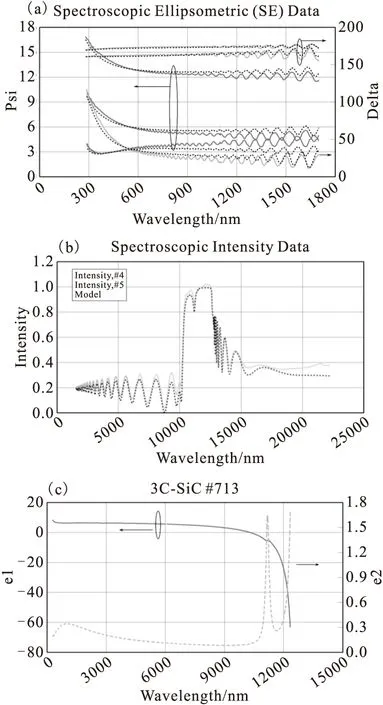
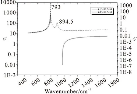
For 3C-SiC grown on silicon,dielectric function of Si substrate is well understood.We can use three general oscillators to simulate absorptions above band edge,and phonon modes are in the range of 600 cm-1to 6000 cm-1which is the range of interest in FTIR.We use dielectric function of cubic silicon carbide measured by Palik[12]etc.as an initial value.Then the film thickness is roughly adjusted to match the interference fringe in the range of 1000 nm to 10000 nm,which stretch over the two types of measurement(Fig.1).Four general oscillators are carefully added and adjusted (Fig.2),first two of them are related to bandgap profile,and the other two connected to the dip in the Reststrahlen band and an obviously more intense oscillation just beyond the Reststrahlen band.Automatic fitting procedure gives the final result shown in Fig.2.The two phonon modes are at 793 cm-1and 894 cm-1,with the given amplitude and broadening(Fig.3).

Fig.1 (a) VASE spectra,(b) FTIR spectra and (c) dispersion relation of 3C-SiC on Si

Fig.2 Model and oscillators used in 3C-SiC on Si (#3C713)

Fig.3 Phonon modes derived from TRPL data fitting
The phonon mode in 894 cm-1is not reported in most SiC papers; we also found it to be weaker than the TO mode at 793 cm-1by more than ten order of magnitude,and this mode can be weaker or disappeared when measured at oblique incident angle.We are still trying with some theoretical methods (like first principle) to find out the origin of this weak mode.

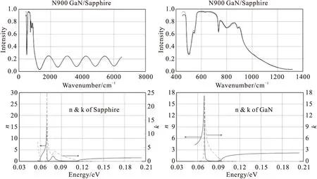
Fig.4 FTIR spectra and dielectric function of GaN on Sapphire

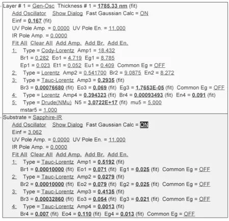
Fig.5 Model and oscillators used in GaN on Sapphire (#N900)
For GaN on sapphire,we start from a simulation of bulk sapphire sample which is also measured by FTIR.Since dielectric function of commercial sapphire is well known,we use then&kin the database,ranging from 250 nm to 1000 nm as starting values.Then we use the Cauchy model to spread the value to infrared range,disregarding the phonon modes.
Until now,the modeled FTIR data is nearly a straight line in the infrared range.We can add oscillators,called Tauc-Lorentz to simulate the phonon modes.After several times of fitting,we can get the final parameter fit to the experimental data well (Fig.4,Fig.5).
Now we have precisen&kdata in the infrared range,where each phonon mode represents absorption of an oscillator.We can use it as a base model in GaN / sapphire structure,and just fix the parameter before making fine adjustment.As the dielectric function of GaN is also well investigated,we can use the results from various references as a starting point.Then,as shown in Fig.5,we use two oscillators (1 and 2) to model the GaN bandgap around 3.4 eV,and the other three modes to simulate LO phonon mode,TO phonon mode and free carrier absorption.
After several fitting procedures,we can get the parameters with sufficiently small mean square error.Two phonon modes,559 cm-1and 736 cm-1represent the LO and TO modes respectively.In fact,these two modes can be identified from the original spectrum,which shows two dips at the corresponding wavenumbers.From Drude model we can deduce the free carrier concentration of around 3×1017cm-3,which is comparable with Raman scattering result (not shown here).
6 Conclusion
We have shown two examples to illustrate the powerful method of using transfer matrix with a combination of different techniques that give similar results.This method is especially in the characterization of material properties.This method is suitable for various kinds of thin film materials even though in this paper we focus on wide bandgap semiconductor thin films.We can get film thickness and dispersion relation reliably,and then deduce the absorption oscillation mode in the ultraviolet-visiable region and infrared region.
Acknowledgment
The work at National Taiwan University was supported by Ministry of Science and Technology under contract No.NSC 102-2221-E-002-191-MY3 and NSC 98-2221-E-002-015-MY3.
Reference
[1] Yeh P.Electromagnetic propagation in birefringent layered media[J].J Opt Soc Am,1979,69:742-756.
[2] Yeh P.Optics of anisotropic layered media:a new 4×4 matrix algebra[J].Surf Sci,1980,96:41-53.
[3] Schubert M.Polarization-dependent optical parameters of arbitrarily anisotropic homogeneous layered systems[J].Phys Rev B,1996,53:4265-4274.
[4] Schubert M.Theory and application of generalized ellipsometry,in Handbook of Ellipsometry[M].New York:Springer,2005:637-717.
[5] Fujiwara H.Spectroscopic ellipsometry principles and applications[M].Hoboken:John Wiley & Sons Ltd,2007:158-176.
[6] Forouhi A R,Bloomer I.Optical dispersion relations for amorphous semiconductors and amorphous dielectrics[J].Phys Rev B,1986,34:7018-7026.
[7] Jellison G E,Modine F A.Parameterization of the optical functions of amorphous materials in the interband region[J].Appl Phys Lett,1996,69:371-373.
[8] Meneses D D S,Malki M,Echegut P.Structure and lattice dynamics of binary lead silicate glasses investigated by infrared spectroscopy[J].Journal of Non-Crystalline Solids,2006,352:769-776.
[9] Tiwald T E,Thompson D W,Woollam J A,etal.Application of IR variable angle spectroscopic ellipsometry to the determination of free carrier concentration depth profiles[J].Thin Solid Films,1998,313:661-666.
[10] Tanguy C.Analytical expression of the complex dielectric function for the Hulthén potential[J].Phys Rev B,1999,60:10660-10663.
[11] Feng Z C,Yang T R,Hou Y T.Infrared reflectance analysis of GaN epitaxial layers grown on sapphire and silicon substrates[J].Materials Science in Semiconductor Processing,2001,4:571-576.
[12] Palik E D.Handbook of Optical Constants of Solids[M].New York:Academic Press,1985.
Characterization of Optical Properties of Wide Band Gap Semiconductor Thin Film with the Combination of Ellipsometry and Infrared Spectrum
XIE Deng1,2,QIU Zhi-ren2*,WAN Ling-yu3,TIN Chin-che4,5,MEI Ting6,FENG Zhe-chuan3
(1.InstituteofOptoelectronicMaterialandTechnology,SouthChinaNormalUniversity,Guangzhou510631,China;2.StateKeyLaboratoryofOptoelectronicMaterialsandTechnologiesandSchoolofPhysics,SunYat-SenUniversity,Guangzhou510275,China;3.CollegeofPhysicsScience&Technology,GuangxiKeyLaboratoryfortheRelativisticAstrophysics,Laboratoryofoptoelectronicmaterials&detectiontechnology,GuangxiUniversity,Nanning530004,China;4.DepartmentofMechanicalEngineering,UniversityofMalaya,50603KualaLumpur,Malaysia;5.DepartmentofPhysics,AuburnUniversity,Auburn,Alabama36849,U.S.A.;6.TheKeyLaboratoryofSpaceAppliedPhysicsandChemistry,MinistryofEducationandShaanxiKeyLaboratoryofOpticalInformationTechnology,SchoolofScience,NorthwesternPolytechnicalUniversity,Xi’an710072,China)
Wide band gap semiconductor films,including silicon carbide (SiC),gallium nitride (GaN),zinc oxide (ZnO) and their compounds and isomers,posess a band gap larger than 3.2 eV,and the characteristic phonon peak lies between 100 and 1500 cm-1.There are many methods to determine the band width and the characteristic phonon peaks,such as photoluminescence,Raman scattering and optical transmission spectraetc. Here we propose a combination of spectroscopic ellipsometry and Fourier transform infrared reflection spectrum analysis by transfer matrix method,which can determine the dispersion spectra and film thickness simultaneously,ranging from ultra-violet (around 250 nm) to far infrared (about 22000 nm).We construct an optical function model based on harmonic oscillator,and demonstrate that the model is suitable for simulating the resonance absorption of incident light with various wavelengths.
spectroscopic ellipsometry; Fourier transform infrared spectroscopy; transfer matrix method
2015-06-15; 修改稿日期:2015-09-21
中山大学光电材料与技术国家重点实验室开放课题,国家自然科学基金(11474365,61377055,61176085);广东高校国际科技合作创新平台项目(gjhz1103);广西相对论天体物理重点实验室广西自然科学基金创新团队项目(2013GXNSFFA019001),国家自然科学基金(AE0520088)
谢灯(1988-),男,博士,从事宽禁带半导体材料表征分析研究。E-mail:xiedeng5@126.com
丘志仁(1963-),男,副教授,主要从事超快激光脉冲产生技术和时间、空间及光谱分辨技术与应用,半导体材料光物理及器件研究等。E-mail:stsqzr@mail.sysu.edu.cn
1004-5929(2016)03-0214-06
O433.3,O484.5
A
10.13883/j.issn1004-5929.201603004

