An mmWave Dual-Band Integrated Substrate Gap Waveguide Single Cavity Filter with Frequency Selectivity
Qiuhua Lin ,Dongya Shen ,Lihui Wang ,Zhiyong Luo,3,4,*
1 School of Electronics and Communication Engineering,Sun Yat-sen University,Shenzhen 518107,China
2 School of Information Science and Engineering,Yunnan University,Kunming 650091,China
3 Pengcheng Laboratory,Shenzhen 518107,China
4 Shenzhen Key Laboratory of Navigation and Communication Integration,Shenzhen 518107,China
Abstract: A novel dual-band ISGW cavity filter with enhanced frequency selectivity is proposed in this paper by utilizing a multi-mode coupling topology.Its cavity is designed to control the number of modes,and then the ports are determined by analyzing the coupling relationship between these selected modes.By synthesizing the coupling matrix of the filter,a nonresonating node(NRN)structure is introduced to flexibly tune the frequency of modes,which gets a dualband and quad-band filtering response from a tri-band filter no the NRN.Furthermore,a frequency selective surface (FSS) has been newly designed as the upper surface of the cavity,which significantly improves the bad out-of-band suppression and frequency selectivity that often exists in most traditional cavity filter designs and measurements.The results show that its two center frequencies are f01=27.50 GHz and f02=32.92 GHz,respectively.Compared with the dual-band filter that there is no the FSS metasurface,the out-of-band suppression level is improved from measured 5 dB to 18 dB,and its finite transmission zero(FTZ)numbers is increased from measured 1 to 4 between the two designed bands.Compared with the tri-band and quadband filter,its passband bandwidth is expanded from measured 1.17%,1.14%,and 1.13%or 1.31%,1.50%,0.56%,and 0.57%to 1.71%and 1.87%.In addition,the filter has compact,small,and lightweight characteristics.
Keywords: coupling topology;frequency selectivity;non-resonating node(NRN);out-of-band suppression;single ISGW cavity filter
I.INTRODUCTION
There will be more high band spectrums available when people determine and allocate the 5G mm-wave frequency band [1].With the concept proposed of the 6G network,the design of high-performance mmwave filters has become important for the application of satellite tracking filtering,including the low insertion loss design at the mm-wave band [2–4],the multi-band [5–7],high miniaturization [8–10],and frequency selectivity[11–17].The above design has attracted more and more attention.
Solving the above design difficulties,to a degree,can provide a solution for the 5G frequency band and low loss of components.In [2–4],some mmwave bandpass filter components were proposed by using the ridge gap waveguide (RGW) technology[18].They have a low insertion loss (IL) advantage.However,they also have some problems such as large volume and heavy weight because they were designed by directly coupling multiple single-mode resonating cavities and using full-metal material.In[8,9,11],some miniaturized multi-band bandpass filter components were proposed by using the substrateintegrated waveguide (SIW) technology [19].However,the multi-band design of these filters still needs to couple multiple SIW cavities,which would lead to large insertion loss because of these substrate cavities.
The significance of designing more FTZs of the filter components is to improve the poor suppression between two working bands,poor frequency selectivity,and poor suppression of out-of-band.It is not difficult to find that in [2–4] and [8–11],and these filters do not have the function of frequency selectivity without an additional design processing on the waveguide,such as designing slots on the SIW [9–11].In [12–16],the FTZs of these filters are designed to improve the frequency selectivity and out-of-band suppression.In[12,13],a method introducing more FTZs was proposed by studying the coupling relationship of the cavity modes at the input and output ports.
In[14–16],the FTZ of the filter was designed by introducing the negative coupling that was generated by cutting slots on the wall of the SIW cavity.The advantage of these designs is that FTZs were designed without perturbing the in-band response.However,its disadvantages are that the design of shape and the determination of size become complicated,resulting in low controllability of frequency selectivity.In [17],the integrated substrate gap waveguide (ISGW) [20–22]technology is used to design more FTZs.The ISGW is used to package the SIW filter to get two FTZs that are designed on both sides of the passband,which improves the frequency selectivity and out-of-band suppression of the filter.However,this method would increase the profile size and IL of the filter.Presently,it has been noted through investigation that designing the wide surface of the filter as an FSS metasurface with substrate gap to obtain out-of-band FTZs has not been reported.
An improved dual-band single ISGW filter is proposed in this paper,as shown in Figure 1.The work of this paper is as follows: In Section II,a dualband filtering coupling topology with one FTZ in each passband edge is proposed.To design the filter with the above coupling topology,based on ISGW technology,a tri-band filter is designed without introducing an NRN structure.Then the NRN structure is introduced to control the frequency of cavity modes,which moves the two high-order cavity modes to a passband to achieve a dual-band bandpass filter,and then to improve the out-of-band suppression level,an FSS metasurface is creatively introduced as the upper wide surface of its cavity,which designs more out-ofband FTZs between two operating bands.In Section III,the coupling relationship is verified by a calculated coupling matrix,and then the flexibility of frequencies moving and bandwidth are discussed to achieve an improved dual-and quad-band filter,respectively.In Section IV,a summary of this paper is given.
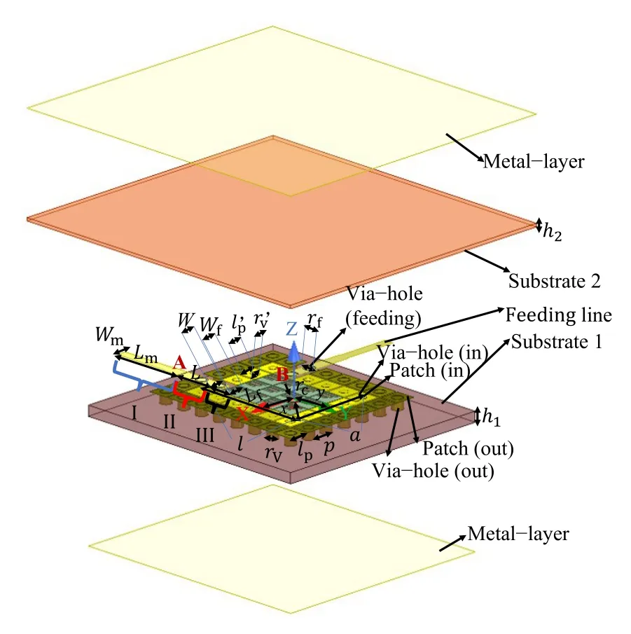
Figure 1. The 3-D structure of the proposed filter.
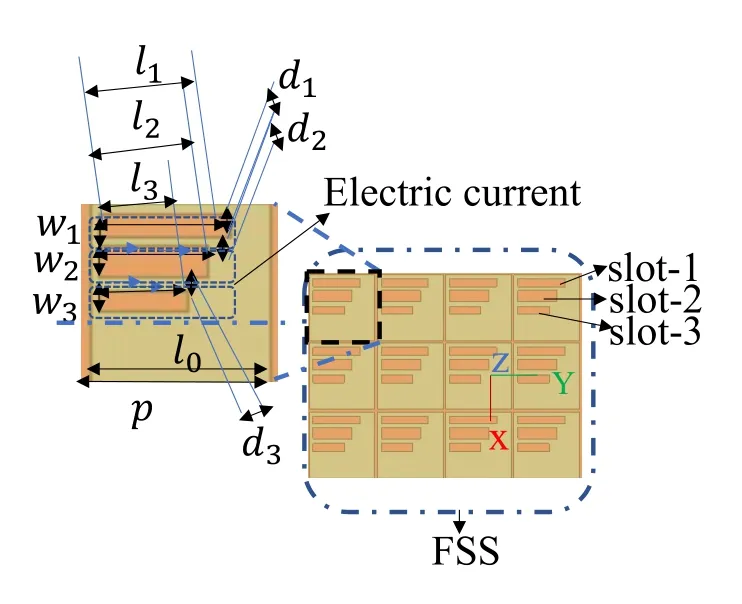
Figure 2. The introduced FSS structure.
II.THE ANALYSIS AND DESIGN OF THE FILTER
As shown in Figure 1,the proposed filter consists of substrate 1 (Rogers RO4003,Relative Permittivity εr=3.38,Dielectric Loss Tangent δ=0.0027)and substrate 2(Rogers RT5880,εr=2.2,δ=0.0009)where substrate 1 is punched with two rows of periodically metalized mushroom-shaped holes along the X-and Y-direction forming the four walls in the Z-direction of the cavity and is printed a metal layer on its lower surface forming the lower wide surface.Substrate 2 is printed with a metal layer on its upper surface,and on its lower surface corresponding to the cavity,an FSS with three slots slit on the unit is printed.The substrate 2 structure(including the substrate 2,metal layer,and the FSS)constitutes the upper surface of the cavity.A metalized hole is punched in the cavity to design the NRN structure.The feeding structure of the proposed filter that is designed at the A and B ports of the cavity consists of three coplanar conductors,including a microstrip line with a characteristic impedance of 50 Ω(also i.e.I),a transmission line of the ISGW(also i.e.II),and a microstrip line feeding into the cavity(also i.e.III).All notations that will be used throughout this paper are shown in Tab.1 and Tab.2.
The design parameters of the FSS structure are shown in Tab.2.
2.1 Design Principle
Different from traditional techniques such as cascade or parallel resonator such as resonant split ring and cavity,a new method that designed a multiple band filtering response in a single cavity by tuning cavity modes coupling relationship is proposed in this paper.The proposed coupling topology with dual-band filtering response is shown in Figure 3.There are a nonresonating node (i.e ➀) in the stopband,a resonating node (i.e ➁) in the 1st passband,and two resonating nodes (i.e ➂and ➃) in the 2nd passband.Node ➀shows a positive coupled relationship with node ➁,➂,and ➃at the source port,and an FTZ at the lower edge of the 1st and 2nd passband will be got [12],repectively.At the load port,node ➁can be negatively coupled with ➀,and node ➂can be negatively coupled with ➃,as a result,another FTZ at the upper edge on the two passbands will be got [13],respectively.TheNRN node between two passbands is designed to control the cross-coupling between the NRN and the cavity modes.So that it can flexibly control the higherorder modes to obtain a dual-band filtering response with a wide bandwidth,or a quad-band filtering response with more passband numbers compared with a single order filtering response.
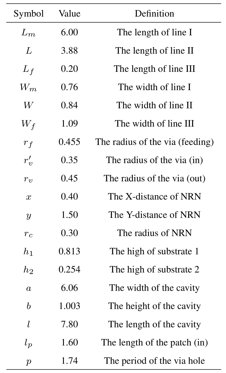
Table 1. The design parameters of the filter(Units: mm).
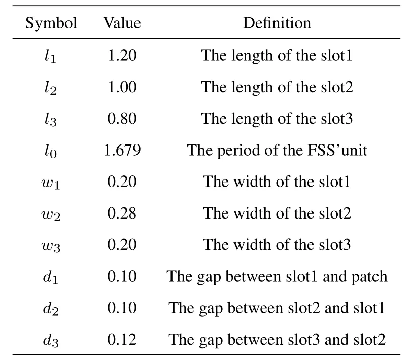
Table 2. The design parameters of the FSS(Units: mm).
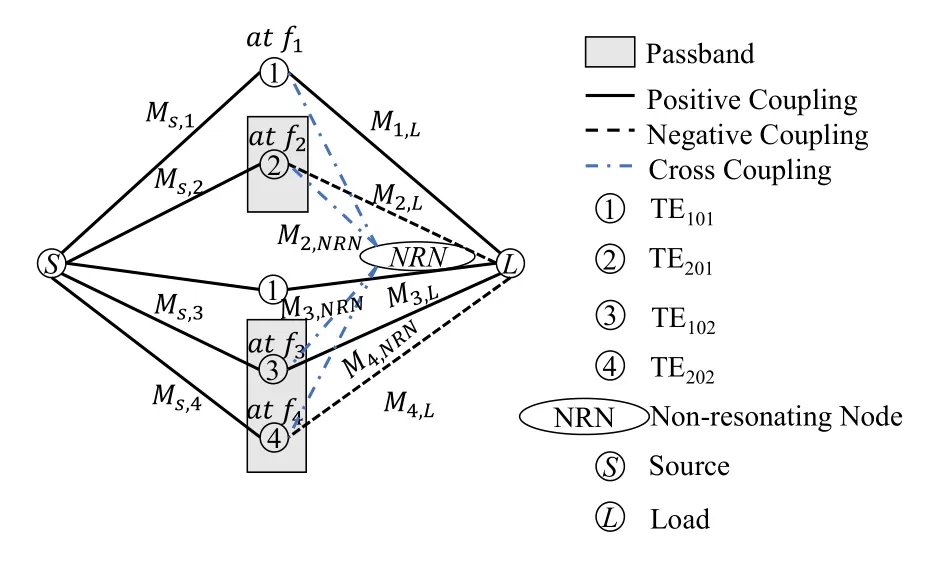
Figure 3. The proposed coupling topology.
2.2 Design and Analysis of the Filter
To fully describe how to use the principle to design the proposed filter,in this section,the design process will follow the procedure,as shown in Figure 4.
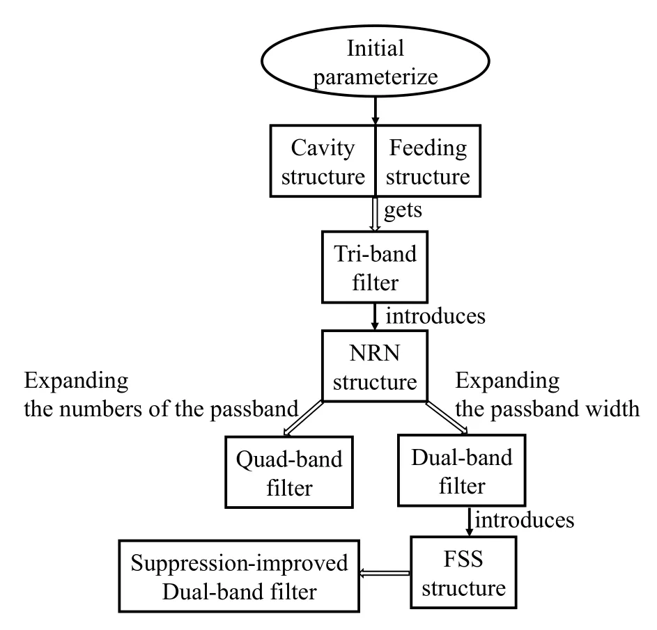
Figure 4. The design process of the proposed filter.
First,the cavity is designed by using the resonant frequency formula that applies to the design of the ISGW cavity,and then the coupling relationship between these different cavity modes is analyzed to determine the locations of input and output ports.Then the feeding structure is further designed to obtain a tri-band bandpass filter without introducing an NRN structure.The NRN structure is introduced to control the cavity modes which makes the resonant modes move to their respective passband to obtain a quadband bandpass filter which controls the higher-order cavity modes to a passband to achieve a dual-band bandpass filter.Finally,to improve the out-of-band suppression level without damaging the in-band response,an FSS metasurface is creatively introduced as the upper wide surface of the cavity to design the out-of-band FTZs.
In Step 1,cavity structure design.An electromagnetic wave with a resonate wavelength λ propagates in the ISGW waveguide.Define the broad side of the cavity as a,the narrow side as b,and the length of the cavity as l.The resonant frequency formula (1) is as follows while a=5b[21]:
where,fomnqis the resonate frequency of the TEmnqmodes,n=0,1,2,...,m=0,1,2,...,q=0,1,2,...,εris the dielectric constant value,µ is permeability constant.According to this equation,the cavity is designed and solved by using the Eigenmode solver of the CST to get the H-plane magnetic field diagram of modes,as shown in Figure 5 (a): there are TE101,TE201,TE102,and TE202four modes in the cavity.A,B,C,and D four ports are given along the cavity wall,so as to study the positions of input and output ports of the feeding line to realize the coupling topology proposed in this paper.
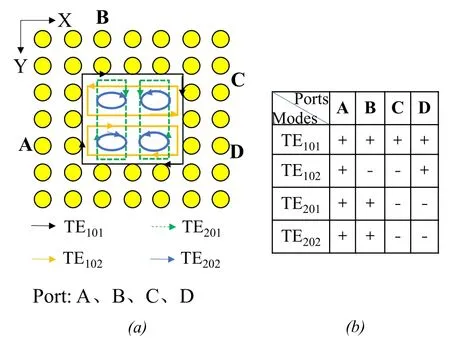
Figure 5.(a)The electromagnetic diagram of cavity modes.(b)The coupling relationship of the cavity modes.
Generally,it is defined that the same direction of magnetic flow is positive coupling (+) and the different direction is negative coupling(-).Then according to Figure 5(a),the mode coupling relationship of the four ports can be sorted out,as shown in Figure 5(b).It shows that(1)TE101is positive coupling(+)in four ports;(2) TE201is positive coupling (+) in A/B ports and is negative coupling(-)in C/D ports;(3)TE102is positive coupling(+)in A/D ports and is negative coupling (-) in B/C ports;(4) TE202is positive coupling(+) in A/B ports and is negative coupling (-) in C/D ports.
Using the coupling topology proposed in this paper to design a filter with more FTZs as well as compact and small circuit size features,the scheme that the input port is laid in A port and the output port is laid in B port is a better choice.
In Step 2,feeding structure design.According to the above analysis,the feeding structure is designed,and it consists of a microstrip line including I,II,and III three parts where part II has been punched two via holes,as shown in Figure 1.Then it is integrated with the cavity to achieve the filter with the proposed coupling topology relationship characteristic.
The filter has been modeled and solved by using HFSS to achieve a tri-band bandpass filtering response with only one mode in each passband.Meanwhile,the ISGW structure that has the same design parameters as those used to design filters in this paper but no cavity is also solved.Their S-parameter values are postprocessed,as shown in Figure 6.
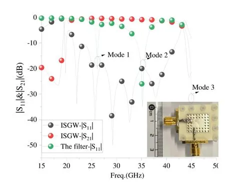
Figure 6. The S-parameters of the ISGW and tri-band filter(Without the NRN structure).
From Figure 6,it can be found that when there is a cavity in the ISGW,three different frequency modes required in this paper are limited in the frequency stopband band gap(FSG)of the ISGW:20.0~40.0 GHz.These three modes form three operating bands with only one mode in their operating bands,and their operating center frequencies are f01=26.0 GHz,f02=35.1 GHz,and f03=45.0 GHz,respectively.Corresponding to fractional bandwidths(FBWs)are FBW1=1.17 %,FBW2=1.14 %,and FBW3=1.13 %,respectively.
In order to verify the coupling relationship and more clearly know the electrical specification of this filter,its coupling matrix M is needed to synthesize,as shown in equation (2).Equation (2) includes all element values between nodes: Source and Load (i.e.S and L),parasitic node ➀,resonating ➁at 1st passband,resonating ➂and ➃at 2nd passband,and a nonresonating node (i.e.NRN) where Mi,jis i,jth element of the coupling matrix M.In general,M is arbitrary and has no structure.However,M can be structured if the filter has some specific or regular geometries.
According to the reciprocity of passive networks,there is Mi,j=Mj,i.Using the proposed conclusion in the reference[12,13],the cross-coupling values are zero,i.e.,M1,2=M1,3=M1,4=0,M2,3=M2,4=0,and M3,4=0.For the solving of Ms,k,k=1,2,3,4;ML,k,k=1,2,3,4,and the self-coupling Mi,i,i1,NRN,can be extracted from the transmission equation S21when the FTZs,the resonating nodes,and the quality factor (Q value) of the filter are determined.For the solving of self-coupling: M1,1,and MNRN,NRN,it can get from equation(3):
where the f0is the center frequency,and fiis the resonating frequency including a non-resonating frequency at stopband.Then an FTZ at the lower edge of the 1st passband will be get by tuning the node TE101(i.e.➀).
In Step 3,NRN structure design.As shown in Tab.1,the NRN structure is a metalized via hole,and its the design parameters are x,y,rc.The relationship between the position and radius of NRN with the cross-coupling value Mi,NRNis shown in reference [23].There are Mi,NRN=MNRN,i,Mi,NRN=-MNRN,j[15],and Mi,NRNcan get from equation(4)[15]:
where the fNRNis a non-resonating node frequency at stopband.MNRN,NRNcan get from equation (4).It can be found from reference [23] that at -3 mm≤x or y ≤-2 mm,the coupling of Mode2becomes stronger with the increase of the x value,and it becomes weaker with the increase of the y value so that it is beneficial to control the interval between two resonating modes.Does this analysis to other resonating modes.And at 2 mm ≤x or y ≤3 mm,the conclusion is opposite.Therefore,the position and radius rcof the NRN are designed by analyzing the crosscoupling Mi,NRNbetween the cavity mode and the NRN,so these higher-order modes are independently controlled to obtain a dual-band filtering response.
In Step 4,after completing the above design,the filter (without FSS structure,see Figure 2,is finally designed,as shown in Figure 1.Its main design parameters are shown in Tab.1.It has been modeled and solved to get its simulated S-parameters by using HFSS and then is fabricated to measure it by using a vector network analyzer.Finally,get the simulated(Sim.) and measured(Mea.) [23]S-parameter results of the filter,as shown in Figure 7.
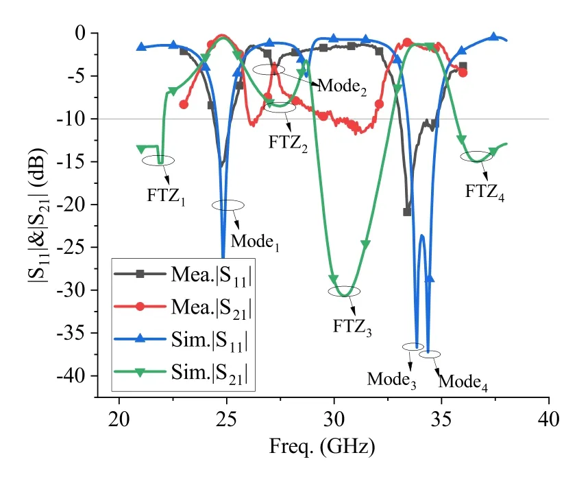
Figure 7. The simulated and measured S-parameter results of the filter.
From the Figure 7,it can be seen that the operating bands of the filter are 24.75~25.10 GHz and 33.35~34.51 GHz which have one mode (i.e.Mode1) in 1st and two modes (i.e.Mode3and Mode4) in 2nd passband,respectively,and in addition,there is a spurious band (i.e.Mode2).Its center frequencies are f01=24.80 GHz and f02=34.00 GHz,and FBWs are FBW1=2.02%and FBW2=3.41%,respectively,which are more wide bandwidths in each band compared with the tri-band filter.In its out-of-band,there are FTZ1=22.5 GHz,FTZ2=27.5 GHz,FTZ3=31.5 GHz,and FTZ4=36.5 GHz four FTZs.The above measured and simulated results are in good agreement.
In Step 5,introduce the FSS structure.It is easy to find that there is a spurious band between two designed passbands,as shown in Figure 7.In fact,it is generated due to not matching to Mode2but matching to Mode1,which greatly reduces the out-of-band suppression of the first passband.
For solving the above important problem that also often occurs in most traditional cavity filter designs and measurements[10,13,15]to improve the out-ofband suppression and enhance frequency selectivity,two works have been done in this paper.For the one,assume that an improved dual-band filter has a center frequency f0=GHz,fNRN=31.50 GHz,and FBW1=1.70 %,according to equation (4),the relationship of M2,NRNand f2is in Figure 8.From this figure,it can be found that when the frequency f2of the Mode2equal to 27.5 GHz,M2,NRNequal to 0.12,therefore,it can realize by designing the NRN structure with 2rc=dc=0.55 mm,then matching to it by optimizing the parameters Wm=0.76 mm,W=0.84 mm,Wf=1.09 mm,Lf=0.20 mm,etc.
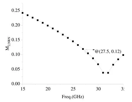
Figure 8. The relationship of M2,NRN and f2.
For the other,the FSS metasurface,as shown in Figure 2,is creatively introduced as the upper wide surface of the cavity to design the out-of-band FTZs for achieving good frequency selectivity and improving the out-of-band suppression level but without damaging the in-band response.
In case of normal incidence,the simplified equivalent circuit model of the designed FSS is given in Figure 9.When an X-polarized plane wave is normally incident upon the structure,two Y-directed sides of these three slots act as plates of capacitors,respectively,that these capacitors(i.e.C1,C2,and C3)play with parallel relationship,whereas the two Y-directed sides act as inductors (i.e.L1,L2,and L3),respectively,that these inductors play with series relationship,which constitutes the series L-C resonator.Simultaneously,the X-directed sides of the along three slots support axial electric current,thus acting as inductors (Ls) that are parallel with the series L-C resonator.In addition,the surplus part of the patch still constitutes the music parallel LpCgresonator.The dielectric substrate supporting the structure is considered as a short transmission line whose length is lT=h2,and wave impedance is ZT=Z0⁄(εr1/2).The free space at both sides of the FSS structure is modeled as transmission lines with characteristic impedance of Z0=377 Ω.
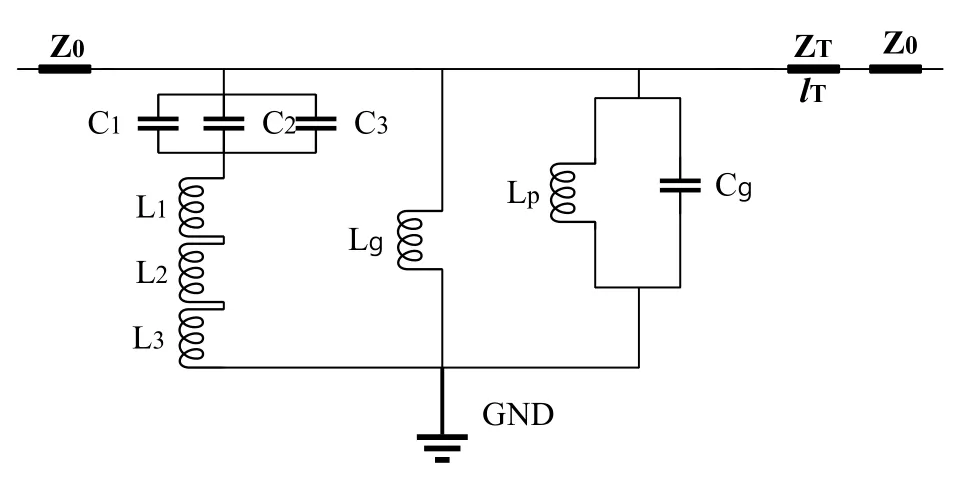
Figure 9. Equivalent circuit model of the designed FSS shown in Figure 2.
Based on the duality theorem[24],the approximate relationship between the effective values of Lpand Cgand the design parameters of the FSS is provided,the capacitance Cgis given by equation (5) in reference[25]:
where ε0and εrare the permittivity of the free space and the relative permittivity of the dielectric substrate,respectively.εeff=(1+εr)/2 is the effective permittivity of the medium.g=(p-l0)/2.Correspondingly,the hybrid resonator (Lpand Cg) and the series L-C resonator determines the two stopbands,respectively,and their frequencies satisfy the following formulas:
where FTZ3and FTZ4are the operating frequencies of the two stopbands,the calculation equation(6)and(7).The reactance of the inductance and the susceptance of the capacitance can be calculated from equation(8)and(9)in reference[26]:
where i=1,2,3,λz1is the wavelength of the first stopband,and the F function has the same expression as described in reference[26].
Through completing the above work,compared with the filter shown in Figure 7,it has been matched to Mode2for designing a passband(@27.5 GHz)but Mode1has been moved to the parasitic band(@22.0 GHz)and not matching to it,and two FTZs have been introduced between the two designed bands,their operating frequencies are FTZ3=29.45 GHz and FTZ4=30.67 GHz,respectively.Finally,an improved dualband filter has been designed,as shown in Figure 1.
III.RESULTS AND DISCUSSION
The coupling matrix has been got,as shown in equation(10),for the 1st passband,M1,1=36.50 ≫M2,2=0.097,satisfies the requirement proposed in the reference[12].At the same time,M1,L=0.224,and M2,L=-1.05 ≤0 satisfies the requirement proposed in the reference[13];for the 2nd passband,M1,1=36.50 ≫M3,3=-0.089,M4,4=-0.094 satisfies the requirement proposed in the reference[12],M3,L=0.330 ≥0,and M4,L=-0.360 ≤0 satisfies the requirement proposed in the reference[13].The coupling relationship is consistent with the required positive or negative coupling for the mode coupling from Figure 3.So there will get an FTZ at the lower and upper side of each passband.
The filter with the FSS structure also has been modeled and solved.Finally,its simulated S-parameter results are got,as shown in Figure 10.
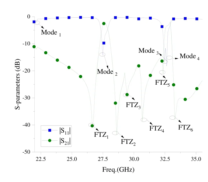
Figure 10. The simulated S-parameter results of the filter with the FSS structure.
From this figure,it can be seen that the operating bands of the filter are 27.39~27.86 GHz with one mode (i.e.Mode2),and 32.26~32.87 GHz with two modes (i.e.Mode3and Mode4),and at the same time there is a spurious band (i.e.Mode1@ 22.0 GHz) because its mode impedance does not matched it.Its center frequencies are f01=27.50 GHz and f02=32.52 GHz,respectively.In its out-of-band,there are FTZ1=26.64 GHz,FTZ2=28.61 GHz,FTZ3=29.45 GHz,FTZ4=30.67 GHz,FTZ5=32.35 GHz,and FTZ6=33.29 GHz six FTZs in its out-of-band.Compared with the filter without the FSS metasurface structure,the out-of-band suppression level from measured 5 dB improves to 18 dB,and its FTZ numbers increase from measured 1 to 4 between the two designed bands.Therefore,the out-of-band suppression level and frequency selectivity get great improvement without damaging the in-band response.Compared with the tri-band filter,its passband bandwidth increased from 1.17%to 1.71%in the 1st band,and from 1.13%to 1.87%in the 2nd band,which has been expanded by moving two high-order modes to one passband.
However,as above analysis of the equation(4)and the results shown in reference,the NRN structure can realize a flexible design to tune the frequency of modes,which moves Mode3and Mode4to their passband,respectively.Then their mode impedances are matched to design a quad-band filter that has only one mode in each band.Because there is no other structure would be introduced,so the NRN structure and some important design parameter values such as Lm=6.5 mm,L=4.03 mm,W=Wf=1.026 mm,x=0.6 mm,y=0 mm,and rc=0.455 mm are changed,but with other same design parameter values compared with the previous improved dual-band filter are taken.The above filter has been modeled and solved to get its simulated S-parameters by using the HFSS.Finally,gets the simulated S-parameters results of the filter,as shown in Figure 11.
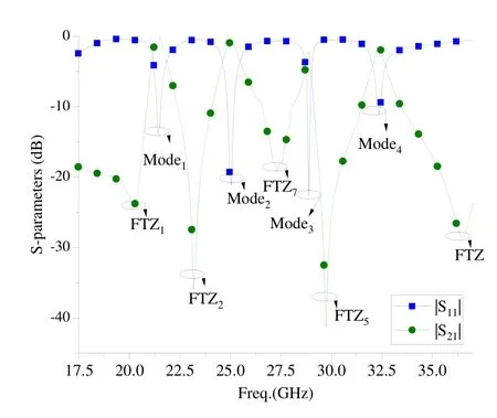
Figure 11. The simulated S-parameter results of the quadband filter designed from the filter of Figure 1.
From Figure 11,it can be seen that the operating bands of the filter are 21.30~21.58 GHz,24.76~25.14 GHz,28.7~28.88 GHz,and 32.26~32.44 GHz with only one mode in each passband.Its center frequencies are f01=21.44 GHz,f02=25.33 GHz,f03=28.80 GHz,and f04=32.30 GHz,respectively,its fractional bandwidths are 1.31%,1.50%,0.56%,and 0.57 %.There are FTZ1=20.27 GHz,FTZ2=23.08 GHz,FTZ7=27.29 GHz,FTZ5=29.73 GHz,and FTZ6=36.94 GHz five FTZs.It needs to note that there is added a new FTZ7=27.29 GHz according to the design principle.
At the same time,because it has been changed the design parameters:Ls=6.5 mm,L=4.03 mm,W=Wf=1.026 mm,which does not match the impedance of FSS structure so that do not generate FTZ3and FTZ4.Compared with the previous dual-band filter,it has been expanded two passbands.
The multi-band filters in recent years are compared in terms of design technology (i.e.Tech.column),center frequency (i.e.f0column),insertion loss (i.e.IL column),Out-of-band suppression level (i.e.Sup.column),cavity numbers of filter(i.e.Num.column),and size of the filter (i.e.Size column),as shown in Tab.3.
It can be seen from the Tab.3 that two center frequencies of the proposed filter are f01=27.50 GHz and f02=32.92 GHz,respectively,and its insertion loss (ILs) are IL1=1.91 and IL2=2.01 dB in each passband,respectively,which has a higher operating frequency bands compared to the design proposed in the reference [7],[10],and reference [15],but its insertion loss does not be worse and is small at every passband in-band,relatively.To design FTZ1,FTZ2,and FTZ6three FTZs in this paper,just needs to design the input and output ports according to the coupling relationship between cavity modes,which does not introduce any other additional design structure such as need additional sliting slot in the reference [7] and[11],or does not need combining with two technologies [15] and [17].Therefore,there are more lower design complexity and fewer technologies are needed in this work.Compared with the filters proposed in the reference[2]and[4],the out-of-band suppression level is relatively bad due to existing the substrate cavity loss but is better than the reference [4],[15] and[17]designed also by using the dielectric substrate materials.In addition,the dual-band filtering response is designed by tuning the multiple modes in one single cavity,which there are two advantages: (1) less substrate insertion loss for needing fewer substrate cavity numbers compared with the reference[7],[10]and reference [15];and (2) a more smaller volume and more lighter quality compared with the reference[2],[4],and the reference[17].
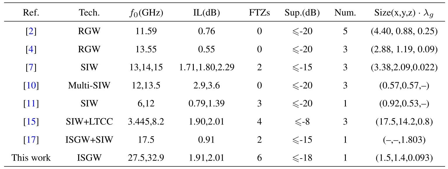
Table 3. Comparisons with the presented works in references.
IV.CONCLUSION
An mmWave dual-band ISGW cavity filter is proposed in this paper with mark frequency selectivity.The cavity modes of the filter are flexibly controlled to move frequency of the modes.According to this,a dualband filter with wider bandwidth and a quad-band filter with more bands and only one mode in-band have been designed.An FSS with three slots to each patch is creatively designed as the upper surface with a substrate gap of the cavity of the filter.Its center frequencies are f01=27.50 GHz and f02=32.92 GHz,respectively.Corresponding to the passband bandwidth,it increases from measured 1.17 %,1.14 %,and 1.13% of the tri-band filtering response or 1.31 %,1.50%,0.56 %,and 0.57 % of the quad-band filtering response to 1.71%and 1.87%.There are six FTZs in its out-of-band.Compared with the filter without the FSS metasurface,the out-of-band suppression level from measured 5 dB improves to 18 dB,and its FTZ numbers increase from measured 1 to 4 between the two designed bands.In addition,the requirement for a compact,small size,and lightweight filter structure has been realized in this paper.The filter component is suitable for the application of satellite tracking filtering.
ACKNOWLEDGEMENT
This work was supported by the National key research and development program of China (No.2021YFB2900401),and by the National Natural Science Foundation of China (No.61861046),the key Natural Science Foundation of shenzhen(No.JCYJ20220818102209020),and the key research and development program of shenzhen (No.ZDSYS20210623091807023).
- China Communications的其它文章
- Design Framework of Unsourced Multiple Access for 6G Massive IoT
- 6G New Multiple Access Technology
- OFDMA-Based Unsourced Random Access in LEO Satellite Internet of Things
- Cluster-Based Massive Access for Massive MIMO Systems
- A Joint Activity and Data Detection Scheme for Asynchronous Grant-Free Rateless Multiple Access
- The Extended Hybrid Carrier-Based Multiple Access Technology for High Mobility Scenarios

