Single-Layer Symmetrical Full-Port Quasi-Absorptive Filtering Phase Shifter
Qingxiang Dong ,Yongle Wu,* ,Weijuan Chen ,Yuhao Yang ,Weimin Wang
1 School of Integrated Circuits,Beijing University of Posts and Telecommunications,Beijing 100876,China
2 School of Electronic Engineering,Beijing University of Posts and Telecommunications,Beijing 100876,China
Abstract: In this article,a single-layer symmetrical full-port quasi-absorptive filtering phase shifter is presented.The proposed phase shifter is composed of a main quasi-absorptive filtering branch,a reference quasi-absorptive filtering branch,and two delay lines.The proposed phase shifter achieves both phase controlling function and quasi-absorptive filtering function for the first time.Each quasi-absorptive filtering branch can realize the quasi-absorptive filtering function.Meanwhile,the constant phase shift can be obtained by combining the two quasi-absorptive filtering branches and the two delay lines.The design formulas can be derived from the even-and odd-mode network analysis,and then two quasi-absorptive filtering phase shifters can be devised easily and quickly.For verification,a 90°quasi-absorptive filtering phase shifter,which is critical for circularly polarized antenna systems,is simulated,manufactured,and measured.
Keywords: filtering;phase shifter (PS);quasiabsorptive;reflectionless;symmetrical
I.INTRODUCTION
In the past decades,radio frequency(RF)systems have developed rapidly.As key components of RF systems,phase shifters have attracted much attention from researchers.Different types of phase shifters,such as Schiffman phase shifters [1,2],broadside-coupled phase shifters[3,4],stub-loaded phase shifters[5,6],reflection-type phase shifters [7–9],and so on,are widely applied to phased arrays,beamforming networks,Doherty power amplifiers,modulators,and many other RF systems.The bandwidths of Schiffman phase shifters[1,2]are hard to improve due to the difficulty of achieving tight coupling for edge-coupled lines.In[3]and[4],broadside-coupled phase shifters can realize tight coupling easily and avoid such problems.However,these broadside-coupled phase shifters need two or more layers,which increases the complexity and incompatibility of the systems.The single-layer phase shifter in [5] can also achieve broadband performance by loaded stubs.Reflectiontype phase shifters[7–9] can provide tunable phase shifts,which is hard for other types of phase shifters.Therefore,reflection-type phase shifters are urgently needed when tunable phase shifts are required.
Because of the ability of reducing circuit size and insertion loss (IL),multi-functional RF devices are more attractive than traditional RF devices [6],[10–19].In[6],[18],and [19],filtering phase shifters are proposed,which transfer the signal in the passband and reflect the signal back to the input port during the stopband.This filtering principle may cause problems when filtering devices are connected to nonlinear circuits [20].Therefore,absorptive (reflectionless) filtering devices are presented in [10],[11],and[20–24],which can protect RF systems from the undesired reflected signals.Nevertheless,researches about the absorptive filtering phase shifters are scarce.Therefore,a single-layer symmetrical full-port quasiabsorptive filtering phase shifter is proposed for the first time.As shown in Figure 1,the proposed quasiabsorptive filtering phase shifter can achieve filtering and phase controlling functions independently instead of the combination of the absorptive filter and traditional phase shifter.Before this article,there are no such quasi-absorptive filtering phase shifters,which can eliminate the undesired reflected signals.The circuit structure of the proposed quasi-absorptive filtering phase shifter is exhibited in Figure 2.This phase shifter is simpler and more compatible for its singlelayer structure.The presented quasi-absorptive filtering phase shifter is composed of the main quasiabsorptive filtering branch(QAFB),reference QAFB,and two delay lines.Because of the symmetrical structure,this single-layer filtering phase shifter can easily realize the quasi-absorptive performance at each port.By combining the two QAFBs with two delay lines,the phase shifting function can be realized.The analysis and design of the proposed phase shifter are provided in Section II.According to even-and oddmode network analysis in[25],the design formulas of the presented filtering phase shifter can be obtained.Based on these design formulas,the proposed quasiabsorptive filtering phase shifter can be devised.In Section III,an example is simulated,manufactured,and measured for demonstration.Finally,conclusions are discussed in Section IV.

Figure 1.The application advantages of single-layer symmetrical full-port quasi-absorptive filtering phase shifters.
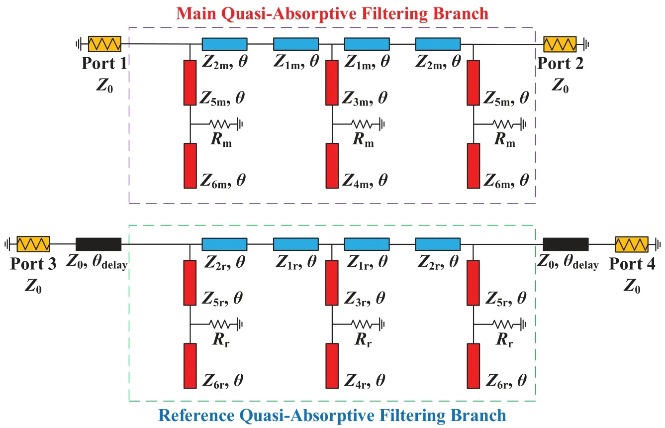
Figure 2.The circuit structure of the proposed quasi-absorptive filtering phase shifter.
II.ANALYSIS AND DESIGN
The circuit structure of the single-layer symmetrical full-port quasi-absorptive filtering phase shifter is shown in Figure 2,which possesses four ports.The main line occupies ports 1 and 2.The reference line occupies ports 3 and 4.Figure 3 exhibits the evenand odd-mode equivalent circuits of the QAFB,which are derived from the even-and odd-mode analysis approach in [25].Ris the value of the resistances.Zi(i=1,2,3,4,5,and 6) andθare the characteristic impedances and electrical lengths of the transmission lines in Figure 3.In this article,θis set as 90° at the center frequency (f0).The characteristic impedance and electrical length of the delay lines areZ0andθdelay.The relationship between frequency(f)and electric length(θ)can be expressed as whereθ0andθdelay0are the electrical lengths corresponding to the center frequency.
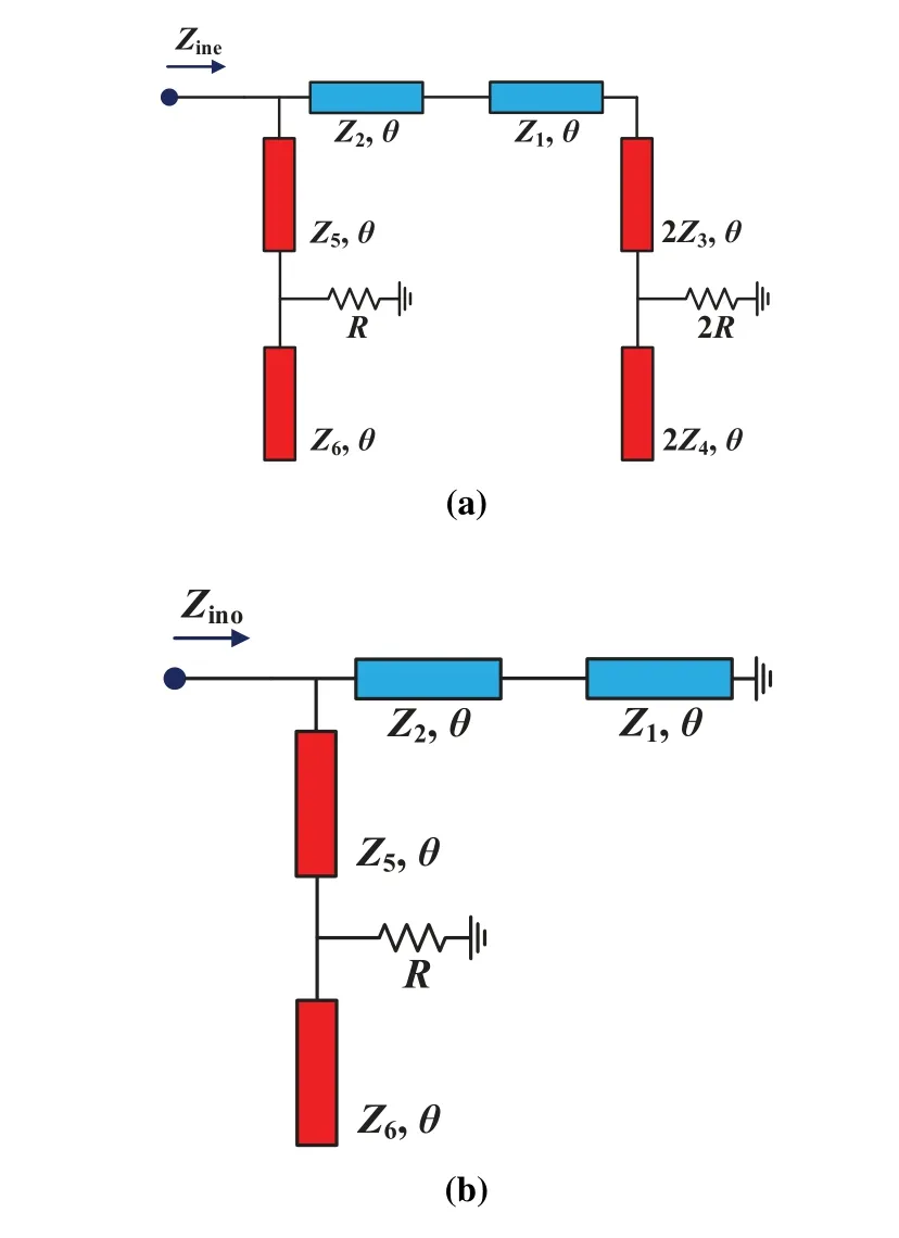
Figure 3.The equivalent circuits of the QAFB under (a)even-and(b)odd-mode excitations.
2.1 Analysis for QAFB
As shown in Figure 2 and Figure 3,the QAFB is formed by a pass way and three absorptive stop ways.The pass way is composed of four transmission lines(Z1andZ2).By using four transmission lines,better absorption and bandwidth can be realized.The three stop ways are composed of six transmission lines(Z3-Z6)and three grounded resistances(R).The structure of stop ways is simple and easy to analyze.By using three stop ways,better absorption and phase controlling can be obtained.In passband,signals can be transmitted through the pass way.In stopband,signals will enter these stop ways and be consumed by the grounded resistances instead of reflected back to the input port.In this way,the QAFB can achieve the quasi-absorptive filtering function.As shown in Figure 3,ZineandZinocan be derived as
wherek1,k2,andk3are calculated as
Based on[25],theS-parameters can be expressed as
Based on(3a)and(3b),theS-parameters of the QAFB can be expressed as
whereg5-g10can be expressed as
2.2 Analysis for the Proposed Filtering Phase Shifter
According to the circuit structure in Figure 2,theS-parameters of the main line can be derived from(4a),(4b),and(4c)as
whereZimandRmcorrespond toZiandR(i=1,2,3,4,5,and 6).
Similarly,theS-parameters of the reference line can be derived from(4a),(4b),and(4c)as
whereZirandRrcorrespond toZiandR(i=1,2,3,4,5,and 6).
Based on(5c)and(6c),the phase shift(ΔΦ)of the presented filtering phase shifter can be defined as
In this article,Φ0is representative of the needed phase shift value,which can be defined as the phase shift at the center frequency(f0).The phase error(Φe)between ΔΦ and Φ0can be expressed as
By analyzing equations (1)-(8),the characteristics of the proposed filtering phase shifter can be mastered.At the center frequency,the phase shift is determined by the electrical length of the delay lines,which means Φ0is associated withθdelay0as
For the main and reference line,the minimum return loss(RL)and the maximum insertion loss(IL)can be obtained by utilizing Matlab.In this article,andrepresent the main and reference line minimum RL.represent the main and reference line maximum IL.
In this article,the phase-shift bandwidth can be defined as
Then, after a hasty breakfast, he went to gather Beauty s rose, and mounted his horse, which carried him off so swiftly that in an instant he had lost sight of the palace, and he was still wrapped in gloomy thoughts when it stopped before the door of the cottage
Similarly,the 1-dB bandwidth can be defined as
2.3 Design of the Proposed Filtering Phase Shifter
Herein,a 45°quasi-absorptive filtering phase shifter is analyzed and calculated as an example to briefly describe the design steps.Here,Z0,Rm,andRrare both 50 Ω.According to(9),theθdelay0can be determined.Φ0is 45°andθdelay0is 22.5°.For the 45°phase shifter,the RL should be more than 15 dB during 0.25-1.75(normalized frequency) for both the main and reference line,which meansshould be better than 15 dB.The maximum out-of-band suppressions should be better than 20 dB,which means the out-of-bandare better than 20 dB.The maximum phase error(Φemax)and phase-shift bandwidth should be better than 3° and 50 %.In this article,the range of the characteristic impedances is 45-125 Ω.The design process for characteristic impedances is exhibited in Figure 4.First,the initial values of characteristic impedances are given.Then characteristic impedances vary in range to find the numerical solutions by utilizing Matlab.
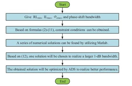
Figure 4.The design flow chart for characteristic impedances.
According to the simple design steps above,a 45° quasi-absorptive filtering phase shifter can be achieved.In a similar way,a 90°quasi-absorptive filtering phase shifter can also be realized.The theoreticalS-parameters and phase shifts of the two designed phase shifters are shown in Figure 5 and Figure 6.To prove universality,normalized frequency is taken to plot Figure 5 and Figure 6,which means the proposed phase shifter can be applied in different frequency bands.The corresponding design parameters are exhibited in Table 1.

Table 1.Design parameters.
As shown in Figure 5,the 45°phase shifter can meet the design requirements.The theoretical RL of the main line and the reference line are both more than 15 dB.The theoretical 1-dB bandwidth of the main line and the reference line are 18% (0.91-1.09) and 24% (0.88-1.12).The maximum theoretical lowerand upper-stopband suppressions of the main line and the reference line are 21.15 dB (0.41) &21.15 dB(1.59) and 21.05 dB (0.38) &21.05 dB (1.62).The theoretical phase-shift bandwidth is 50% (0.75-1.25)with Φemaxof 3.21°.
III.SIMULATED AND MEASURED RESULTS
Herein,a 90° quasi-absorptive filtering phase shifter centered at 2 GHz,which is important to circularly polarized antenna systems,is chosen to certificate the theory above.
The 90° quasi-absorptive filtering phase shifter is simulated and optimized by Advanced Design System(ADS).The physical dimensions of the optimized phase shifter are displayed in Figure 7a and Figure 7b.Then,the phase shifter is manufactured on Rogers4350B,whose relative permittivity,loss tangent,and thickness are 3.48,0.0037,and 1.524 mm.The picture of the fabricated phase shifter is exhibited in Figure 7c and Figure 7d.The fabricated phase shifter is measured by an Agilent Network Analyzer.
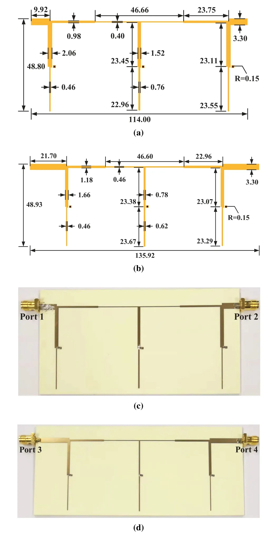
Figure 7.The physical dimensions (unit: mm) of (a) the main line&(b)the reference line and picture of(c)the fabricated main line&(d)the fabricated reference line.
As shown in Figure 8,the simulated and measured results of the 90°quasi-absorptive filtering phase shifter are in good agreement.The differences between them are caused by the losses of SMA and manufacturing errors,which is obvious at high frequencies(3.0-3.5 GHz).The measured results are listed in Table 2.The measured results show that the 90° phase shifter possesses a quasi-absorptive filtering function.The measured phase-shift bandwidth is 55.61%(1.48-2.62 GHz)with the maximum phase error of 2.82°.In the overlapped 1-dB working band (1.76-2.17 GHz),the phase shift is during 87.42°-90.82°,which is defined as the working band of the quasi-absorptive filtering phase shifter.In the working band,the minimum RL and maximum IL are 13.70 dB and 1.52 dB.The comparisons with other reported phase shifters are shown in Table 3.By the way,the calculated and simulated phase deviations are different in Figure 6 and Figure 8,which is mainly caused by the losses of microstrip lines and the errors of the resistances.

Table 2.The measured results of the proposed phase shifter.

Table 3.Comparisons with other reported phase shifters.
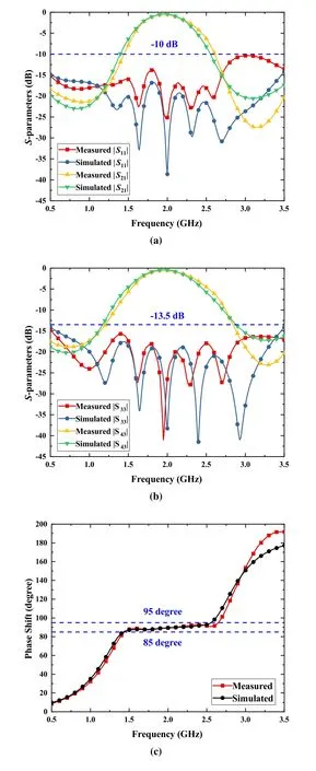
Figure 8.Simulated and measured results of the 90°quasiabsorptive filtering phase shifter: (a)|S11|&|S21|,(b)|S33|&|S43|,and(c)the phase shift.
IV.CONCLUSION
In this article,a single-layer symmetrical full-port quasi-absorptive filtering phase shifter is proposed,which is required by the systems containing nonlinear circuits.By applying the even-and odd-mode analysis approach,the design formulas can be obtained easily and quickly.Based on these formulas,two quasi-absorptive filtering phase shifters have been designed.For demonstration,a 90°quasi-absorptive filtering phase shifter has been simulated,manufactured,and measured.The measured results show that the 90°phase shifter can achieve a good quasi-absorptive filtering function and phase controlling ability.The circuit size is a little large and will be reduced by bending the microstrip lines and introducing coupled lines.In the near future,the presented single-layer symmetrical full-port quasi-absorptive filtering phase shifter will be more and more attractive in RF systems.
ACKNOWLEDGEMENT
This work was supported by National Natural Science Foundations of China (No.U20A20203,No.61971052,and U21A20510),the Fundamental Research Funds for the Central Universities (2021XDA07-1),and Key Research and Development Project of Guangdong Province(2020B0101080001).(Corresponding author:Yongle Wu).
- China Communications的其它文章
- IoV and Blockchain-Enabled Driving Guidance Strategy in Complex Traffic Environment
- LDA-ID:An LDA-Based Framework for Real-Time Network Intrusion Detection
- A Privacy-Preserving Federated Learning Algorithm for Intelligent Inspection in Pumped Storage Power Station
- Secure Short-Packet Transmission in Uplink Massive MU-MIMO Assisted URLLC Under Imperfect CSI
- Multi-Source Underwater DOA Estimation Using PSO-BP Neural Network Based on High-Order Cumulant Optimization
- An Efficient Federated Learning Framework Deployed in Resource-Constrained IoV:User Selection and Learning Time Optimization Schemes

