
High throughput N-modular redundancy for error correction design of memristive stateful logic
2023-02-20 13:16XiZhu朱熙HuiXu徐晖WeipingYang杨为平ZhiweiLi李智炜HaijunLiu刘海军SenLiu刘森YinanWang王义楠andHongchangLong龙泓昌
Chinese Physics B 2023年1期
关键词:海军
Xi Zhu(朱熙), Hui Xu(徐晖), Weiping Yang(杨为平), Zhiwei Li(李智炜),Haijun Liu(刘海军), Sen Liu(刘森), Yinan Wang(王义楠), and Hongchang Long(龙泓昌)
College of Electronic Science and Technology,National University of Defense Technology,Changsha 410073,China
Keywords: memristor,stateful logic,logic reliability,in-memory computing
1. Introduction
Traditional computation system based on the von Neumann architecture separates the computation from storage.Data stored in the storage unit need moving to the processor unit to accomplish the computation tasks. It brings significant costs in time and energy.[1]With the advent of artificial intelligence(AI)and the internet of things(IoT),it is harder for the traditional computation system to meet the requirements of low latency and low energy costs. An in-memory computing system that computes within the storage unit is a promising approach to overcome the challenge.[2]
Memristive stateful logic[3–8]is one of the most promising candidates to realize the in-memory computing. Memristor is a two-terminal nonvolatile electronic device.[9–12]Its resistance state can be switched between the low resistance state(LRS)and the high resistance state(HRS).The switching rule depends on the magnitude and the polarity of the applied voltage on it. The memristor in the memristive stateful logic can work as the computation unit and the storage unit within the integrated crossbar array,[13,14]which can remove the costs for the data movement.
However, current fabrication technology cannot eliminate the randomness of conductive filament (CF) formation/dissolution in the cation-based memristor,which induces that randomness including resistance variations and voltage variations in the SET/RESET operation for the memristor exits inevitably.[15]In the resistance variations, LRS and HRS variation ratesσ/μcan reach 0.01 and 0.07, respectively.[16]And in the voltage variations, set and reset voltage variationsσ/μcan reach 0.034 and 0.027, respectively.[17]These variations may bring the memristive stateful logic with the reliability problems.[18–22]The authors in Refs. [20,21] proposed multiple operations to improve the reliability. But the reliability of the logic may decrease when the device characteristics and the operation times cannot meet the specific conditions.Reference[22]proposed a universal logic error scheme,which requires customization for specific error control including unintended nonswitching of the output cell, unintended switching of the output cell, and unintended switching of the input cell. Besides, when the target logic operation is complex,a balanced gate needs to be designed carefully for the optimal time,area,and energy. Reference[18]proposed an error monitor scheme for an IMPLY-based memristive in-memory computing system. But it can only monitor and correct the specific stateful logic family of IMPLY logic. Reference[19]proposed a scheme which corrects the logic error with the additional memristive logic operations. But the reliability of the additional memristive logic must be credible to improve the reliability of the expected logic.
Therefore,we propose an n-modular redundancy logic error correction scheme with the best universality and throughput. And in comparison with the other two approaches which also need additional CMOS circuits, it needs fewer transistors and cycles for the error correction. Moreover, synthesis and in-memory mapping of logic execution in a single row(SIMPLER)[23]can map a given logical function into a single column (or row) with maximum cell reuse automatically,which can be combined with the full parallel stateful logic computation to realize the scheme design from logical primitives to logical functions.
This paper extends our work in the conference paper,[24]which only proposes the basic n-modular redundancy error correction design with preliminary mathematic simulation results. The major contributions of this paper include:
(i) The reliability of the logic event and the logic function is analyzed, and the implication of the device instability on the logic reliability is discussed. The principle of nmodular redundancy is systematically analyzed. The design of the high throughput n-modular redundancy error correction scheme with a universal design paradigm is proposed.
(ii) An n-modular redundancy error correction circuit is put forward to improve the reliability of the stateful logic. The operational process is presented. And the circuit is simulated with Cadence Virtuoso to demonstrate its function.
(iii)Based on the properties of the tested devices,a case study of the scheme is carried out with HSPICE to evaluate the performance of the 1-bit full adder(FA)based on the stateful neural network.
In this paper, Section 2 presents the full parallel stateful logic based on the stateful neural network in the memristive crossbar array and the definition of the throughput. The reliability of the logic event and the logic function is analyzed,and the implication of the device instability on the logic reliability is discussed in Section 3. The principle and the design of the n-modular redundancy error correction scheme are proposed in Section 4. The 1-bit FA based on the NOR logic and the NOT logic is demonstrated for an example and the analysis on the scheme is presented in Section 5. This paper is concluded in Section 6.
2. Full parallel stateful neural network
Figure 1(a) shows anm×nmemristive crossbar array,wheremWLs andnBLs are connected with the synaptic weights. The configurations of the synaptic weights include one-transistor-one-resistor(1T1R),one-selector(or onediode)-one-resistor (1S(D)1R), and one-resistor (1R). Sneak path[25]through unselected cells in the crossbar array may incur unexpected resistance switching in the logic operation.Therefore,1T1R configuration is adopted in this paper, to alleviate the implication of the sneak path. 1R crossbar arrays presented in this paper are just used to show the function of the crossbar array. The practical realization of the logic operation is based on the 1T1R crossbar array. The voltages can be applied on WLs and BLs. Then the crossbar array can realize the vector-matrix multiplication (VMM) through Ohm’s law and Kirchhoff’s current law (KCL) through a read operation.[26]Figure 1(b)shows the realization of the VMM with the input voltages applied on the WLs and the output currents through BLs. And figure 1(c)shows the realization of the VMM with the input voltages applied on the BLs and the output currents through WLs. In Fig. 1(b), when BLs are connected to the ground directly,we can obtain
When BLs are connected to the grounded resistorsRL,respectively,we can gain
whereVirepresents the voltage applied on thei-th WL;Ijrepresents the current through thej-th BL;Gijrepresents the conductance of the memristor at the intersection of thei-th WL and thej-th BL;GLrepresents the conductance of the load resistorRL.

Fig.1. (a)Memristive crossbar array, including 1T1R configuration and 1S(D)1R configuration. (b)Realization of the VMM with the input voltages applied on the WLs and the output currents through BLs. (c)Realization of the VMM with the input voltages applied on the BLs and the output currents through WLs.
Furthermore,if the resistance states of the memristors in each WL are the same,the voltages applied on memristors in each WL are the same. AndI1=···=Ij=···=In. When the memristors in the crossbar array are the bipolar memristors, namely, they only have two resistance states:RLRSandRHRS,memristors in each BL can be designed as a logic function based on the stateful logic, whereRLRSrepresents logic‘1’ andRHRSrepresents logic ‘0’. We can make use of these characteristics for realizingnsame logic functions simultaneously.
For example,VA,VB, andVCare applied on WL1, WL2,and WL3, respectively. And the other WLs are floating. It can realize the NOR logic based on the stateful neural network in Fig.2(a). Memristors are connected to the grounded load resistorRL. They would not be reset when the voltages between them are positive due to their polarity. The initial state of the output memristor C isRHRS, representing logic“0”. With a high resistance ratio ofRHRS/RLRS,RLRSconductance andRHRSconductance can be normalized approximately as the real numbers 1 and 0,respectively,which allows the logical value and device conductance to be used interchangeably.According to Ohm’s law and Kirchhoff’s law,the node potentialVIcan be deduced as

wherei=A,B,C,andRL,andVRL=0.When the voltageVC–VIexceeds the threshold voltageVset,namely,VC–VI–Vset>0,the output memristor C will be switched toRLRS(logic“1”).

whereYcan be viewed as the weighted sum in a neural network,[5]that is,Y=∑i Giwi.Givalues (the conductance values) work as the input variables andwivalues (wi=VC–Vi–Vset) work as the synaptic weights. Figure 2(b) shows the equivalent network model in Fig. 2(a). Thewi(voltage applied on the memristors) can be adjusted to obtain different outputs (logic output values). Figure 2(c) shows the truth table of the NOR logic. Similarly, figures 2(d), 2(e), and 2(f)show the NOT logic based on stateful neural network,singlelayer perceptron network,and the truth table of the NOT logic,respectively.

Fig.2. (a)The NOR logic based on stateful neural network.[5] (b)Single-layer perceptron network for the NOR logic. (c)The truth table of the NOR logic. (d)The NOT logic based on stateful neural network.[5] (e)Single-layer perceptron network for the NOT logic. (f)The truth table of the NOT logic.
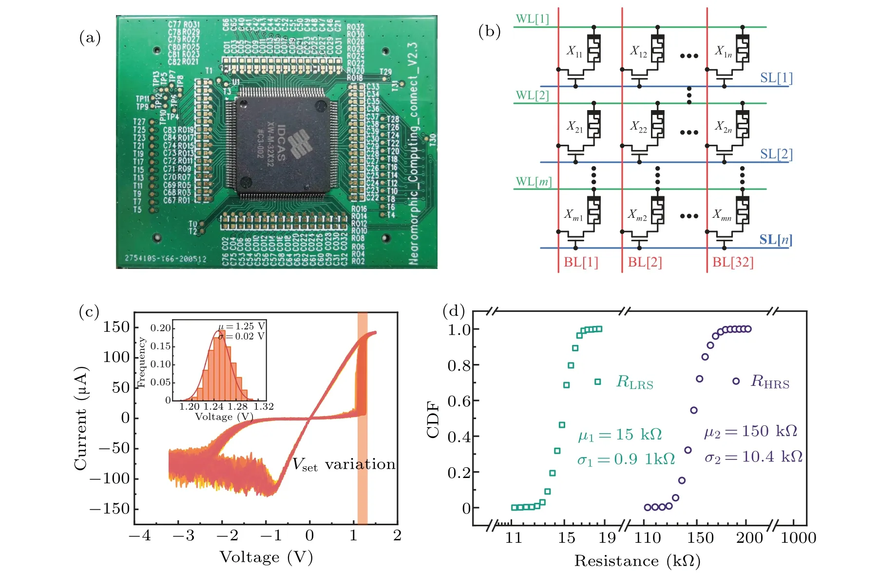
Fig.3. Characterization of TiN/TaOx/HfOx/TiN memristor. (a)Optical image overview of the packaged chip. (b)The schematic of 32×32 1T1R crossbar array inside the chip. (c) I–V characteristics of the TiN/TaOx/HfOx/TiN memristor and the distribution of the set threshold voltage Vset measured in the direct current sweeping test. (d)Cumulative distribution function(CDF)of RLRS and RHRS measured in the pulse test.
To measure the device properties and verify the scheme,the circuit-level platform with the TiN/TaOx/HfOx/TiN 1T1R 32×32 crossbar array and its peripheral circuits are established. Figures 3(a)and 3(b)show the optical image overview of the packaged chip and the schematic of 32×32 1T1R crossbar array inside the chip, respectively. The transistor in the 1T1R array works as a selector to alleviate the implication of the sneak path and a current limiter to perform the compliance current. In the direct current sweeping test,when the selected memristor is set to the LRS, a voltage of 1.5 V is applied on the corresponding SL to open the selected memristor,and the corresponding WL sweeps from 0 V to 1.5 V, while the BL is grounded. When the selected memristor reset to the HRS,a voltage of 1.5 V is applied on the corresponding SL to open the selected memristor, and the corresponding BL sweeps from 0 V to 3.2 V,while the WL is grounded. The typicalI–Vcharacteristics of the bipolar memristor is shown in Fig.3(c). And the normal distribution of the set threshold voltageVsetwith the mean valueμ=1.25 V and the standard deviationσ=0.02 V is also presented in Fig. 3(c). In the pulse test, a voltage of 1.5 V is applied on the selected SL. And the set voltage and the reset voltage are 1.25 V and-2 V, respectively. The cycles are 1000. The cumulative distribution function(CDF)ofRLRSandRHRSis shown in Fig.3(d),whereRLRSfollows the normal distribution with the mean valueμ1=15 kΩ and the standard deviationσ1=0.91 kΩ,andRHRSfollows the normal distribution with the mean valueμ2=150 kΩ and the standard deviationσ2=10.4 kΩ.
According to the practical device properties and principles of the stateful neural network mentioned above, the circuit parameters would be configured:RL= 1.25RLRS, andVA=VB=0.6Vset,VC=VN=1.3Vset. The parameters of the device and the circuit are shown in Table 1. Note that the circuit parameters remain unchanged in the simulations and tests.
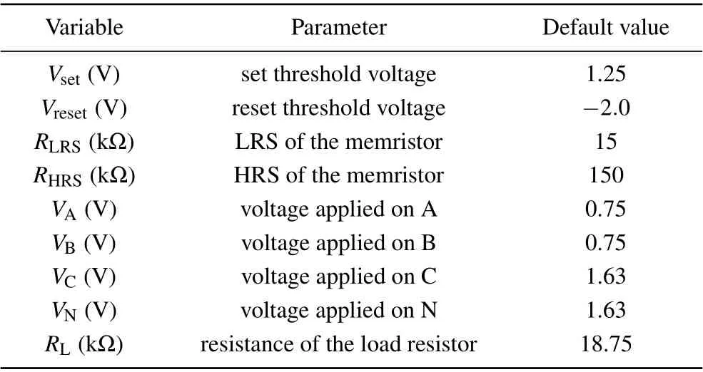
Table 1. Parameter of the device and the circuit.
Furthermore, the throughput, which is the maximum number of instances that can be executed within the crossbar array within a given time unit,is defined as
It can be improved by parallelizing the execution of many instances of the same logic function: each instance is placed in a different column as shown in Fig.1(b).
3. Logic reliability
wherePeirepresents the reliability of the logic eventQi →.
For example, as for 2 input NOR stateful logic gates,there are 4 logic events from the input logic sequencesQ:Q1= [0,0,0],Q2= [0,1,0],Q3= [1,0,0], andQ4=[1,1,0]to the output logic sequences=[0,0,1],=[0,1,0],=[1,0,0],=[1,1,0]. WhenP(=0|Q1=P(=0|Q1)=P(=1|Q1)= 1, the reliability of the logic event IPe1is 1. The characteristics of these memristors are consistent with each other, and the voltages applied on the A and B are the same. Therefore, inputs A and B are equivalent to each other.Moreover,we can divide these 4 logic events into 3 types for the NOR logic. Type I:Q1→,Type II:Q2→, andQ3→, Type III:Q4→as shown in Fig.2(c). Similarly,we can divide 2 logic events into 2 types for the NOT logic. Type I:Q1→, Type II:Q2→as shown in Fig.2(f).
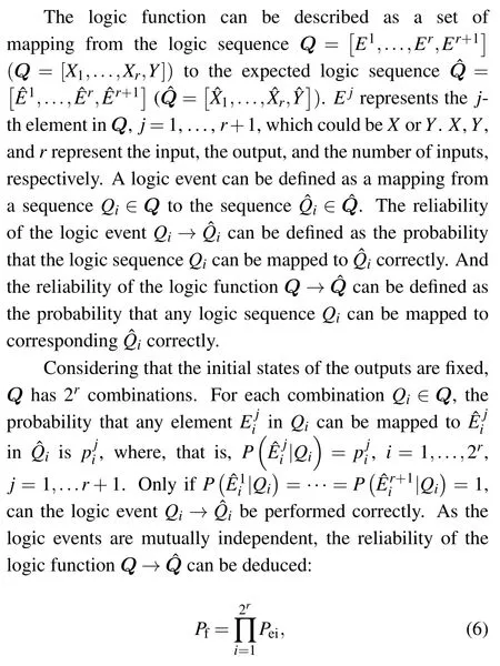
The implication of device instability on the reliability of the logic events in the NOR logic and the NOT logic is simulated as shown in Figs. 4(a) and 4(b). The circuit parameters are shown in Table 1. The device parameters(Vset,Vreset,RLRS, andRHRS) fluctuate appropriately based on the tested result. Assuming variableXsatisfies the normal distributionN(Xm,(Xm×rate)2), whereXm, and rate represent the mean value, and fluctuation rate (σ/μ), respectively. For example,rate=0.016 inVset, considering that the mean value ofVsetis 1.25 V, namely,Vset~N(1.25,0.022) (V). Here the devices followVset~N(1.25,0.022) (V),RLRS~N(15,(15×rate)2) (kΩ), andRHRS~N(150,(150×rate)2) (kΩ) independently,and the rate fluctuates from 0.01 to 0.09. The simulation is based on the TEAM model,which is simple,flexible,general,and sufficiently accurate for memristive device-based circuit design.[27]
Figure 4 shows that the reliability of these logic events will keep decreasing as the device instability increases. In Fig.4(a),Q2→,andQ3→decrease synchronously as the device instability increases,which validates that these two logic events can be put into logic event type II together. Type I(Q1→)and type III(Q3→)have the worst and the best reliability in the device instability, respectively. In Fig. 4(b),type I has better reliability than type II initially. And type I decreases faster than type II with the instability increasing.
It demonstrates that device instability has a great impact on the logic reliability. However, device instability is inevitable based on the current fabrication technology. In order to solve such an issue,ann-modular redundancy error correction scheme is proposed to help the memristive stateful logic design towards high reliability.
Fig.4. The implication of device instability on the reliability of the logic events in the NOR logic(a)and the NOT logic(b).
4. Logic error correction scheme
4.1. Principle of the logic error correction scheme
We can make use of the vector–matrix multiplication in the memristive crossbar array to realize the error correction scheme based onn-modular redundancy efficiently. Figure 5 shows ther-input logic error correction circuit design based onn-modular redundancy. It is anm×ncrossbar array whose WLs are connected to the corresponding current comparators CC.The red memristors are in incorrect states in the crossbar array. The green voltagesVreadused for reading the memristors’states are applied on the BL and their currentIDis gathered to the corresponding comparator.
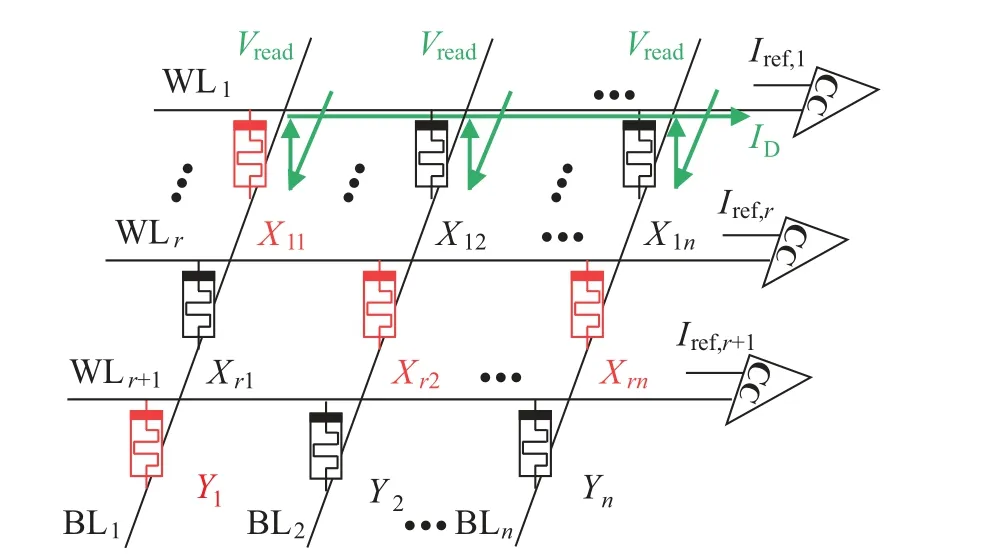
Fig.5. The r-input logic error correction circuit design based on nmodular redundancy.[24]
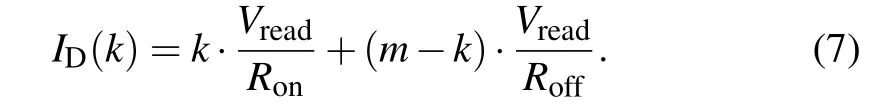
There arensamer-input and logic functions(r+1=m)in the crossbar array. Through applying voltages on the WLS,nlogic functions can be performed simultaneously as a result of the vector-matrix multiplication in the crossbar array. However,some memristors are in the incorrect resistance states due to the instability in memristors.If there arekmemristors are inRLRSand(mk)memristors are inRHRS, whenVreadis applied on BLS,the current through WLIDcan be deduced according to Ohm’s law and Kirchhoff’s current law:
Memristors in the crossbar array are fabricated in the same condition. Therefore, we can assume that they follow the same random distribution independently.

Moreover,the probability thatID≥ID(+1)can be deduced:

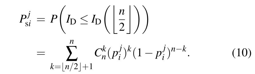
In a single logic event,the relationship between the number of redundancynforreaching the expected reliability andis shown in Fig. 6. It demonstrates that increasingncan increase reliability. Moreover,nwill keep decreasing asincreases continuously and the change rate speeds down asincreases continuously.
If>50%for any,this probability can keep increasing and close to 100%as the number of repeated logic operationsnincreases.


Fig.6. The relationship between the number of redundancy n for reaching expected success rate and pi.[24]
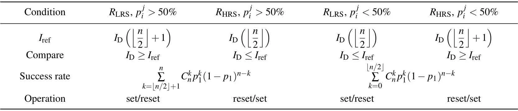
Table 2. The operation based on different conditions.
Therefore, for each element in any logic combination,when the probabilitycan be evaluated,can be promoted throughn-modular redundancy bit by bit. It can enhance the reliability of the logic event. And then the reliability of the logic function can be enhanced according to Eq.(6).
4.2. Design of the error correction scheme
The inequations in Eqs. (9) and (10) can be performed with a current comparator. We can compareIDwithIrefwhich represents the critical current when the number ofRLRSaccounts for half of thenmemristors. IfIDis>Iref, we will applyVseton thesenmemristors to make them inRLRS, or we will applyVreseton them to make them inRHRS,under the condition>50%for any.
Figure 7 shows the universal steps for the error correction scheme based on then-modular redundancy. The red memristors represent the memristors that are in incorrect states. The blue current comparator CC represents the activated current comparator CC.The green and red arrows represent the directions of read voltage(Vread)and write voltage(VsetandVreset),respectively.
There are 2r+2 steps in the whole correction scheme for ther-input logic. It corrects the memristors WL by WL. In each WL includingrinputs and 1 output,we compare the currentIDwithIrefin the first step. Then a write operation on all memristors in the same WL according to the output of the comparator is performed. If it is desired for the reset operation,Vresetis applied on BLs and the corresponding WL is connected to the ground as shown in Fig.7(b). And if it is desired for set operation,Vsetis applied on the corresponding WL,and BLs are connected to the ground as shown in Figs. 7(d) and 7(f). The other WLs are floating.
Figure 8 shows the schematic diagram for the logic error correction based on then-modular redundancy. The green block and the red block represent the input memristor and the output memristor, respectively. And there arerinputs and 1 output in the logic operation. Figure 8(a) shows the universal design and can correct the errors including the input errors and the output errors, which corresponds to Fig. 5. Thensame logic operation can be performed in 1 step. And the logic correction operation is 2r+2, as shown in Fig. 7. It costs(r+1)×nmemristors and 2r+3 clock cycles.
When therinput memristors can be kept in the correct state in the logic operation, the design in Fig. 8(a) costs(r+1)×nmemristors and 3 clock cycles. Therefore,it can be regarded as the time-optimal logic correction design. Furthermore, when therinput memristors can be kept in the correct state in the logic operation,the scheme can be expanded to another two designs. Figure 8(b) shows the area-optimal logic correction design. The logic operation can be performed step by step. It costsr+nmemristors andn+2 clock cycles. Figure 8(c)shows the trade-off logic correction design. Note thatn/dis an integer generally. It costs(r+n/d)×nmemristors andn/d+2 clock cycles. The time-optimal design and the area-optimal design represent the conditionsn=dandd=1 in the trade-off design,respectively.

Fig.7. The r-input logic error correction step based on n-modular redundancy.[24]

Fig.8. The schematic diagram for the logic error correction based on the n-modular redundancy. (a) the time-optimal logic correction design, (b)the area-optimal logic correction design,(c)the trade-off logic correction design.
Figure 9 presents the schematic diagram of the proposedn-modular redundancy error correction circuit in the 1T1R array. It consists of ANALOG TOP composed of the crossbar array and the error correction block,and DIGITI TOP used for controlling the circuit. In the crossbar array, WLs, BLs, and SLs are connected with the WL drivers, BL drivers, and SL drivers, respectively. BLs and WLs are only connected with the 1T1R. Each SL is connected with the gate of the transistor in the corresponding line,which can control the transistor(open or close)through applying voltages(VopenandVclose)on the corresponding line.The WL drivers and the BL drivers can apply different voltages (Vx,Vread,Vset, andVreset) and states(“G”,“Z”,and“F”)on WLs and BLs,respectively.Vxrepresents the applied voltages on the memristors in the logic operations. And the states“G”, “Z”, and“F”represent that the node is grounded, the node is floating, and the node is connected with the grounded resistorRL,respectively.
The error correction block consists of a multiplexer MUX,and a current comparator. And the error correction circuit is the current comparator. The circuit diagram of the current comparator which consists of 14 transistors is as shown in Fig.10.It compares the read currentIDwith the reference currentIrefthrough comparing the current of two branches out1and out2. IfID>Iref,the output signal will be high level signal. Otherwise,the signal will be low level signal.
The current comparator is connected with MUX.Through the selection signal Ctrl L of MUX, the current comparator can be connected with the specific BL or WL. Then the currentIDwill be compared withIref. The output of the current comparator will be transmitted into the DIGITITOP.
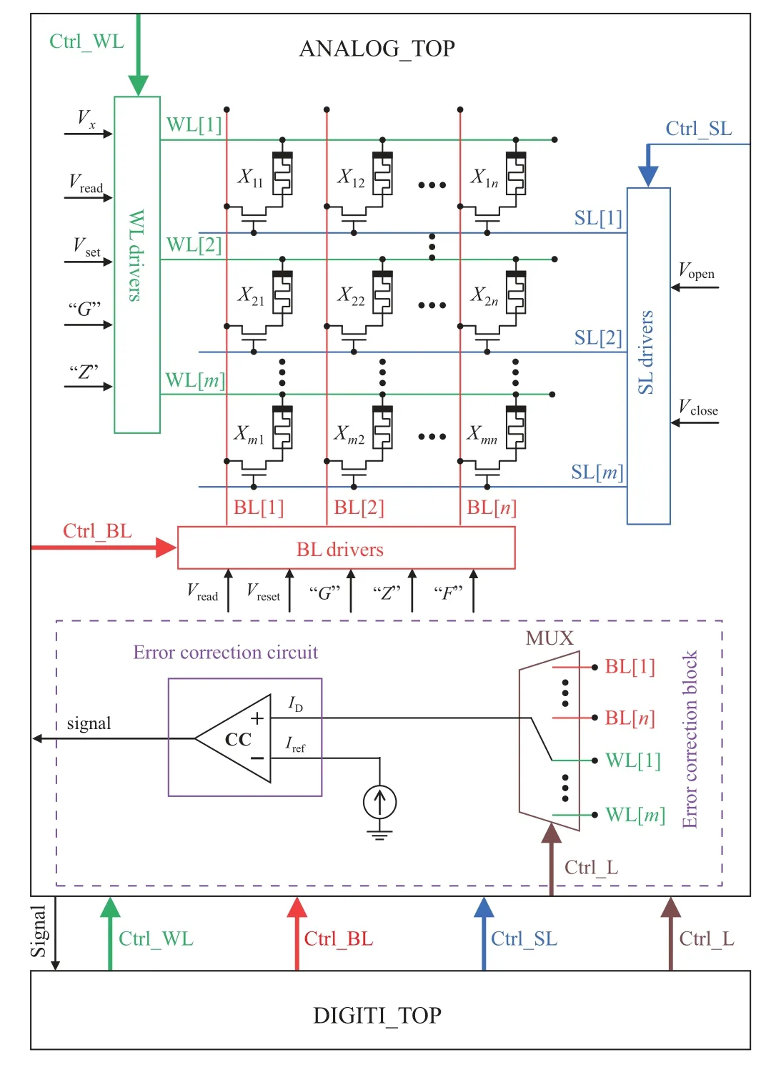
Fig.9. Schematic diagram of the proposed N-modular redundancy error correction circuit in m×n 1T1R array.
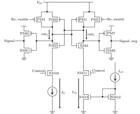
Fig.10. Circuit diagram of the current comparator.
DIGITI TOP can control the crossbar array and the error correction block simultaneously through Ctrl WL, CtrlBL,Ctrl SL,and CtrlL.
We take the NOR logic based on the stateful neural network with 3-modular redundancy for an example to demonstrate the process. When the input memristors can be kept in the correct state in the logic operation,the error correction needs to be performed on the output memristors denoted byX31,X32,andX33.
(i) Perform the logic operation in parallel:WL[1]–WL[3]are applied onVA,VB,andVC,respectively.And the other WLs are in the“Z”state. BL[1]–BL[3]are in the“F”state and the other BLs are in “Z” state.Vopenis applied on SL[1]–SL[3]andVcloseis applied on the other SLs.
(ii) Read the logic states in parallel: WL[3]is connected with the current comparator. And the other WLs are in the“Z”state. BL[1]-BL[3] are applied onVreadand other BLs are in the“Z”state.Vopenis applied on SL[3]andVcloseis applied on the other SLs.
(iii) Write the logic states in parallel:Vopenis applied on SL[3] andVcloseis applied on the other SLs. IfID>Iref,Vsetis applied on WL[3] and the other WLs are in the “Z” state.BL[1]–BL[3]are in the“G”state and the other BLs are in“Z”state; IfID<Iref,Vresetis applied on BL[1]–BL[3], and the other BLs are in“Z”state. WL[3]is in the“G”state and the other WLs are in the“Z”state.
The schematic plot is implemented in the time-optimal logic correction design here. And it also can be implemented in the area-optimal logic correction design. Note that the positions of the applied voltages need to be changed synchronously.
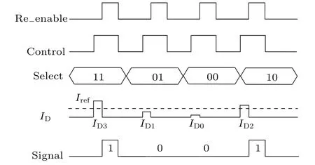
Cadence Virtuoso is utilized to complete the simulation of analog-mixed signal. The memristor model is TEAM model,and the other circuits are based on Semiconductor Manufacturing International Corporation (SMIC) 40-nm technology.Figure 11 shows the output signal of four data patterns with 3-modular redundancy in the NOR logic. re enable and control are the control signal of the current comparator. select represents the different data patterns for 3-modular redundancy.“00” represents that 3 output memristors’ resistance is all in HRS. “01” represents that two output memristors’ resistance is in HRS. “10” represents that one output memristor’s resistance is in HRS.And“11”represents that 3 output memristors’resistance is all in LRS.IDrepresents the read current of the three output memristors. It showsIDis larger thanIrefwhen select is“11”or“10”. And its corresponding output signal is 1. It demonstrates the circuit can work well for the logic error correction.
5. Simulation and discussion
In this section,we take the 1-bit FA as an example to simulate the implication of the device instability on the reliability of the combinational logic circuit. Then the scheme is carried out to improve the reliability of the logic. The 1-bit FA based on the stateful neural network with two steps, whose probability based on the tested result in Fig. 3 is 11.2%, is hard to be realized. Therefore, the 1-bit FA is designed with the NOR logic and NOT logic based on the stateful neural network through multiple steps. With the help of SIMPLER,[23]the 1-bit FA is mapped into a single column within a crossbar array. SIMPLER,short of synthesis and in-memory mapping of logic execution in a single row, can reduce the minimum required number of cells for the execution of the given logical function and reduce the execution latency using a column(or row),which can be combined with the full parallel stateful logic computation to realize the scheme design from logical primitives to logical functions.
5.1. The 1-bit FA simulation
The 1-bit FA based on the NOR logic and the NOT logic within a crossbar array in a single column is proposed according to the SIMPLER. Figure 12(a) shows the 1-bit FA netlist which consists of seven NOR logic gates (g4,g5,g6,g8,g9,g10,andg11)and five NOT logic gates(g1,g2,g3,g7,andg12).Figure 12(b)shows the execution of the 1-bit FA netlist using a single column of the memory with nine memristors.The first three memristors serve as inputs A,B,and Ciand will not be destroyed. The other six memristors are used for the logic operation and the storage of the temporary logic value. There are six steps including 15 clock cycles for the complete 1-bit FA.Step I:initialize the six memristors to logic‘0’(RHRS)for the following logic operation. Step II:serial logic operation of the six gates. Step III:initialize the three memristors not required as inputs for following logic operations. Step IV:serial logic operation of the next three gates. Step V: initialize the three memristors not required as inputs for following logic operations. Step VI:serial logic operation of the last three gates.
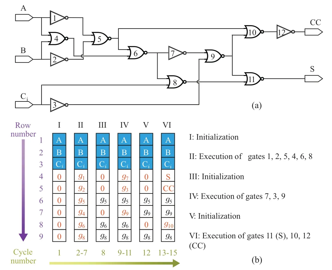
Fig.12.(a)1-bit FA netlist based on the NOR logic gate and NOT logic gate.(b) Execution of the 1-bit FA netlist using a single column of the memory with nine memristors.
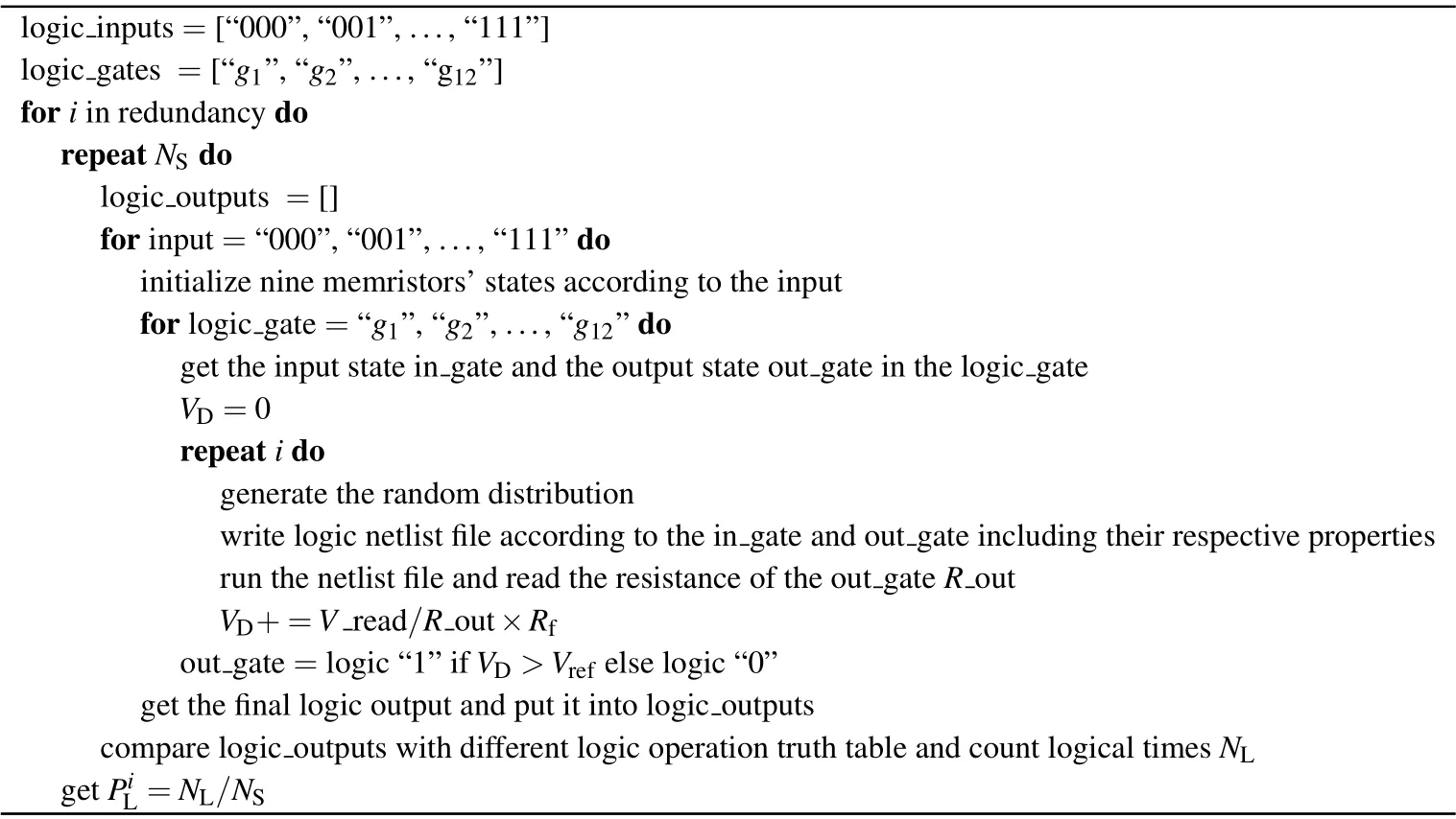
The simulation algorithm ofn-modular redundancy based on the 1-bit FA is demonstrated in Algorithm 1. Note that the states of the input memristors in the logic gates won’t be destroyed in this device characteristics in Table 1. Therefore,the error correction only needs to be carried out for the output cell.
(i) The input such as “000” is obtained from the list logic inputs consisting of[“000”,“001”,“010”,“011”,“100”,“101”,“110”,“111”]. A,B,and Cinare initialized according to the input. The other six memristors are initialized as logic“0”for the logic operation.
Algorithm 1. Simulation algorithm of n-modular redundancy based on the 1-bit FA.
(ii)The 1-bit FA based on thei-modular redundancy circuit is designed, whose memristors’ states are determined by the input. Each memristor follows the same random normal distribution independently. And 12 logic operations are performed in sequence. Accumulate the voltageVDforitimes and compare the voltage with the reference voltageVref. The logic error correction can be executed for the output memristor in every logic operation.After 12 logic operations are finished,the output sequence can be obtained.
(iii) Walk through the input combinations and get the logic outputs. We can compare it with the standard 1-bit FA logic output sequence and count the right logical timesNL.
(iv)Repeat the above steps 1–3 forNStimes,and the reliability of the 1-bit FA based oni-modular redundancy can be calculated:=NL/NS.
(v) Increase the redundancyiand repeat the above steps 1–4. The reliability of the 1-bit FA for different modular redundancies can be obtained.
5.2. Discussion
The probability of the 1-bit FA can be evaluated based on the parameters of the devices and the circuits. Figure 13(a)shows the probability of the logic event[0,0,0,0,0]→[0,0,0,0,0]in the 1-bit FA.When the memristor A is the logic“0”,the probability of the logic event [0, 0]→[0, 1] in the NOT gateg1isPNOT1. Similarly,the probability of the logic events in 12 logic gates and the logic event[0,0,0,0,0]→[0,0,0,0, 0] in the 1-bit FA can be obtained. Furthermore, the other seven logic events in the 1-bit FA are obtained. And the probability of the 1-bit FA can be deduced according to Eq.(6)as shown in Fig.13(b).
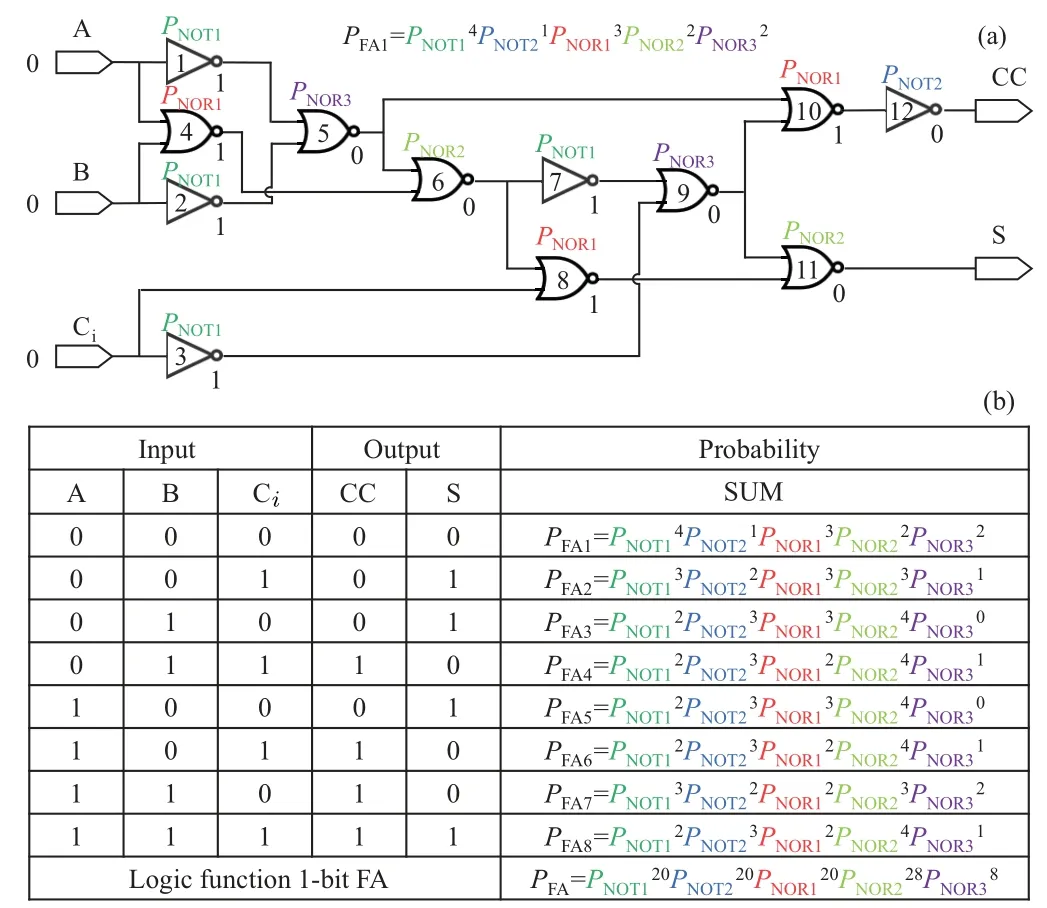
Fig.13. (a)The probability of the logic event[0,0,0,0,0]→[0,0,0,0,0]in the 1-bit FA.(b)Statistics on the number of the NOR and the NOT logic events required by the 1-bit FA logic events.
The probability of the 1-bit FA withn-modular redundancy is simulated and mathematically evaluated, and the results are shown in Fig.14. The devices followVset~N(1.25,0.022) (V),RLRS~N(15,(15×rate)2) (kΩ), andRHRS~N(150,(150×rate)2) (kΩ) independently. S1, S3, S5, and S7 represent the simulation probability of the 1-bit FA with 1,3,5,and 7 modular redundancies,respectively. E1,E3,E5,and E7 represent the mathematical evaluation results of the 1-bit FA with 1, 3, 5, and 7 modular redundancies, respectively.The total simulation timesNS=1000. The rate ofRLRSandRHRSfluctuates from 0.01 to 0.09. It shows the probability of the 1-bit FA decreases as the rate ofRLRSandRHRSincreases.Andn-modular redundancy can improve the probability significantly. What is more,the evaluation results can fit simulation results well,which can verify the evaluation methodology.
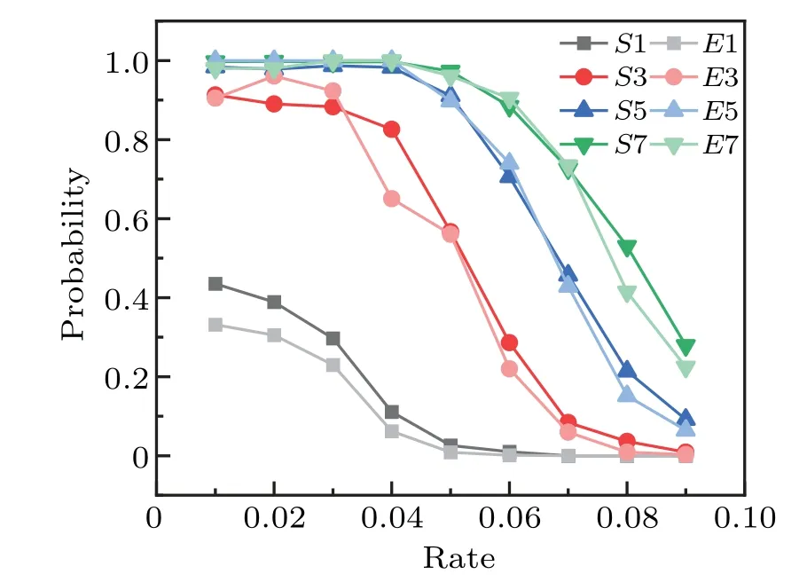
Fig.14. The simulation and evaluation probability of the n-modular redundancy based on the 1-bit FA.
The whole steps can be evaluated in the simulation. The 1-bit FA takes 15 steps, three of which are initialization for following logical operation in Fig. 12(b). The error correction only needs to be carried out for the output cell according to the device characteristics. Therefore, the logical error corrections need to be performed 12 times. If the time-optimal logic correction scheme is carried out where the error correction performs in parallel, the whole steps require 39. And it takes three times of 9, 27 in total, devices among memristive crossbar array.
The throughput of the logic operation with the logic correction can be evaluated. Figure 15 shows all aligned logic column operations with n-modular redundancy oftdifferent row-aligned instances are executed in parallel. And it takes the time-optimal logic correction design. We assume there areasteps for logic operations andbsteps for logic corrections. Then there area+t×bsteps in parallel with the design in Fig. 9. And there are (a+b)×tsteps for the other correction schemes.[17–22]The throughput of this work ist/(a+t×b), which is larger than that of the other correction schemes 1/(a+b)according to Eq.(5).
There are four kinds of error correction schemes[17–22]except for this work. We compare this work with the others from four angles. Table 3 shows the comparison of the error correction scheme.
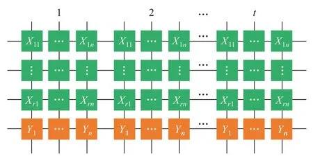
Fig.15. All aligned logic column operations with n-modular redundancy of t different row-aligned instances are executed in parallel.
The authors Refs. [19,20] improved the logic reliability through reasonable multiple operations. Therefore,it does not need additional CMOS circuits. The cycles for error corrections of the primary logic vary from 2–4 according to the devices’properties. It can work for IMP and MAGIC.The logic reliability with it may not be able to reach 100% when the resource consumption is not considered.
Reference [22] divided the logic gates into NOR-type gates and non-NOR-type gates. As for NOR-type gates such as NOR,it makes use of zero checking module(ZCM)consisting of a three-input NOR CMOS logic gate. Three-input NOR CMOS logic gate needs about 6 transistors. As for non-NORtype gates such as NAND,it designs a balance gate consisting of a memristive logic gate to combine these two gates into one logic gate for special detections. Note that the reliability of the balance gate must be 100%. Therefore, before the error correction of the non-NOR-type gate,its balance gate must be corrected first. If the balance gate belongs to non-NOR-type logic gate,it also needs another balance gate to correct the balance gate... When the reliability of the balance gate is 100%,the odd checking module(OCM)consisting of two three-input XOR and one XOR CMOS logic gates is performed to start the error correction. The OCM needs about 16×2×2+16=80 transistors. And the total number of transistors is 6+80=86.And the cycles for error corrections of the primary logic are 3 for NOR-type gates,and at least 6 for non-NOR-type gates.It can work for all kinds of R–R logics. The logic reliability with it always can be able to reach 100% when the resource consumption is not considered.
The authors in Ref.[18]detected two kinds of error types through comparing the node voltages twice,then corrects them with different voltages. The proposed error detection circuit totally requires 72 transistors,where the digital sub-circuits including flip-flops,MUX,and XOR gate,are all designed with the minimized size.[18]And the cycles for error corrections of the primary logic are 4.It can work for IMP.The logic reliability with it always can be able to reach 100%when the resource consumption is not considered.
The authors in Ref.[19]corrected the logic error with the additional memristive logic operations. Therefore,it does not need additional CMOS circuits. The cycles for error corrections of the primary logic are 5. It can work for IMP. The logic reliability with it may not be able to reach 100% when the resource consumption is not considered.
This work judges the correct logic according to the share of different logic values. And the judgment is realized with a current comparator. Therefore,all kinds of logics whose logic values are represented by resistance states are suitable for this work. The current comparator needs 14 transistors. And the cycles for error corrections of the primary logic are 3. It can work for all kinds of R–R logics and V–R logics. The logic reliability with it always can be able to reach 100%when the resource consumption is not considered.
In summary, although these three approaches(Refs.[18,22],and this work)need additional CMOS circuits for improving reliability,the logic reliability with them always can reach 100%when the resource consumption is not considered. The other two approaches cannot. The number of transistors this work needs is observably less than the other two approaches.And the cycles for error corrections of the primary logic of this work needs are less than those of the other two approaches,too. What is more, this work can be suitable for all kinds of R–R logics and V–R logics. Its universality is more powerful than the others.
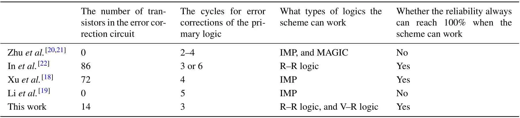
Table 3. Comparison of the error correction scheme.
6. Conclusion
In this paper, we simulated the implication of device instability on the reliability of the logic event with the TEAM model in HSPICE. The mathematical relationship between logic reliability and redundancy has been deduced. Then through combining the mathematical relationship with the vector-matrix multiplication in a memristive crossbar array,the logic error correction scheme has been proposed. It can be implemented in any stateful logic and the logic based on them. Moreover, a universal design paradigm has been put forward for the complex logic with SIMPLER.And the circuit schematic and the flow of the scheme have been raised. Finally,1-bit FA based on the NOR logic and NOT logic within a crossbar array in a single column is simulated and the mathematical evaluation according to the device properties is performed.It demonstrates the scheme can improve the reliability of the logic significantly. And compared with other four error corrections, the scheme which can be suitable for all kinds of R–R logics and V–R logics has the best universality and throughput. Although it needs additional CMOS circuits, the logic reliability with it always can reach 100% when the resource consumption is not considered. And compared with the other two approaches which also need additional CMOS circuits,it needs fewer transistors and cycles for the error correction.
Acknowledgements
Project supported by the National Key Research and Development Plan of the Ministry of Science of Technology of China (Grand Nos. 2019YFB 2205100 and 2019YFB 2205102), the National Natural Science Foundation of China(Grant Nos.61974164, 62074166, 61804181, 62004219, and 62004220),and the Science Support Program of the National University of Defense and Technology(Grand No.ZK20-06).
猜你喜欢
绿色天府(2022年6期)2022-07-14
Chinese Physics B(2022年2期)2022-02-24
军事文摘(2020年22期)2021-01-04
音乐天地(音乐创作版)(2020年7期)2020-09-11
小哥白尼(军事科学)(2018年4期)2018-06-21
军营文化天地(2017年12期)2017-03-01
新闻爱好者(2016年3期)2016-12-01
科普童话·百科探秘(2014年5期)2015-03-09
军事历史(1993年3期)1993-08-21
军事历史(1992年6期)1992-08-15

- Chinese Physics B的其它文章
- The coupled deep neural networks for coupling of the Stokes and Darcy–Forchheimer problems
- Anomalous diffusion in branched elliptical structure
- Inhibitory effect induced by fractional Gaussian noise in neuronal system
- Enhancement of electron–positron pairs in combined potential wells with linear chirp frequency
- Enhancement of charging performance of quantum battery via quantum coherence of bath
- Improving the teleportation of quantum Fisher information under non-Markovian environment