
Optical and electrical properties of BaSnO3 and In2O3 mixed transparent conductive films deposited by filtered cathodic vacuum arc technique at room temperature
2023-02-20 13:16JianKeYao姚建可andWenSenZhong钟文森
Chinese Physics B 2023年1期
Jian-Ke Yao(姚建可) and Wen-Sen Zhong(钟文森)
1College of Materials&New Energy,South China Normal University,Shanwei 516625,China
2Blue Lake Optic-electronic Company,Huizhou 516001,China
Keywords: BaSnO3 and In2O3 mixed film, filtered cathodic vacuum arc deposition, transparent conductive films,microstructure,optical properties,electrical properties
1. Introduction
BaSnO3(BTO)-based transparent conductive films have been exhaustively investigated until now for its wide bandgap with high room-temperature electron mobility and thermal stability.[1,2]For the crystalline temperature of BTO is above 650°C,[3]the BTO-based films are always deposited above 650°C on epitaxy substrate by pulsed laser deposition or molecular beam epitaxy till now to get high quality crystalline which limits their application in low temperature device.
The filtered cathodic vacuum arc (FCVA) technique is an attractive thin film deposition method, which is one of the most promising techniques for high quality semiconductor applications.[4]ZnO and In2O3are typical high performance transparent conductive films which can be deposited by FCVA at low temperature. The optimized polycrystalline indiumtin-doped oxide (ITO) film fabricated on Si (111) substrate by FCVA below 350°C has a high transmittance of 95% in the visible light region, the resistivity is 6.6×10⁻⁴Ω·cm and electron carrier concentration is as high as 1.6×1021cm-3.[5]FCVA technique can cause high temperature in the film surface and high growth rate and high quality crystal growth. Using this technique,500 nm–1300 nm thick and high transparent ZnO:Al films were grown on glass at room temperature(RT) with rates exceeding 250 nm·min-1while maintaining resistivity below 5×10⁻⁴Ω·cm with electron mobility as high as 60 cm2/V·s.[6]
Mixing ZnO in BTO can maintain BTO’s mobility and improve its stability when deposited at low temperature.[7]Indium (In) is usually used as a substituting element for Sn in BTO compound. The induced ferromagnetism and enhanced optical behavior in indium-doped BTO system had been reported due to the relatively non-toxic,easily fusible nature and high mobility, trapping and electron generation rate for In.[8]The photocatalytic efficiency of BTO can be enhanced by In doping as a result of its capability to hinder the electron–hole recombination.[9]Indium is usually used in acceptor substituted BaSn1-xInxO3-yproton conductors.[10–12]In-substituted BTO(BaSn1-xInxO3-y,x=0.125,0.25,and 0.50)compounds were prepared by a gel polymerization method. All compounds were single-phase perovskite structure. The highest proton conductivity of 9.5×10⁻⁴S/cm was obtained for BaSn0.5In0.5O2.75.[12]
However,there are few reports about the optical and electrical properties of In2O3mixed BTO films. With the energetic FCVA technique the poly-crystalline BTO phase can be synthetized at low temperature with improved properties while there are no reports till now. In the article,the microstructure,optical and electrical properties of In2O3mixed BTO films deposited by FCVA technique at RT were investigated.
2. Experiment
The BITO films were deposited by FCVA technique at RT.A cylindrical 80-wt%BTO and 20-wt%In2O3mixed target in diameter of 60 mm and thickness of 5 mm was mounted on a water-cooled copper plate. Typically,the base vacuum of the chamber was 2×10⁻⁶Torr(1 Torr=1.33322×10²Pa)by a two-stage pumping system made of a mechanical roughening pump and a cryogenic pump. The pressure during the deposition was increased to 2×10⁻⁴Torr due to the injection oxygen gas into the chamber. The oxygen gas was introduced into the chamber directly by a mass flow controller with constant flow rate of 50 sccm.The substrates were K9 glasses of thickness of about 1 mm. Prior to loading into the chamber,the substrates were cleaned by ultrasonic bath in acetone,isopropyl alcohol,and rinsed in de-ionized water,and then dried by nitrogen gas.The arc current of 100 A was used for the sample. A toroidal magnetic field around 40 mT was employed to produce the axial and curvilinear fields to steer the plasma.
The structure of film was studied by a Rigaku x-ray diffraction (XRD) meter. The x-ray source used is CuKαradiation at wavelength of 0.15418 nm. The surface morphology of film was studied by a ZEISS Gemini scanning electron microscope(SEM).A Lambda 900 spectrometer was used to measure the transmittance and reflectance of film. To determine the optical constants and thickness of film the Spectroscopic Ellipsometer(SE,Semilab GES5-E)was used.The carrier transportation properties of film was obtained by a Hall system using the van der Pauw configuration (HMS 2000) at RT.
3. Results and discussion
The crystalline phase and crystal orientation are evaluated using XRD. Figure 1 shows the XRD pattern of BITO film on glass substrate. The XRD pattern indicate that the film exhibit a polycrystalline body-centered cubic crystal structure(a=b=c=1.0118 nm) of In2O3clearly. Four peaks appear at 2θ=30.6°,35.4°,50.9°,and 60.6°which correspond to the (222), (400), (440), and (622) directions of the bodycentered cubic crystal structure of In2O3(referred from In2O3XRD standard card number PDF#06-0416). The film also has a polycrystalline perovskite structure of BTO. Peaks appear at 2θ=24.2°, 30.6°, 36.4°, 47.9°, 58.6°, 76.0°, 82.0°,and 89.0°which correspond to the(001),(011),(111),(002),(112), (103), (222), and (213) directions of the perovskite crystal structure of BTO (referred from BTO XRD standard card number PDF#15-0780). The peaks intensity of In2O3are sharp than those of BTO due to its poor crystalline. This is the first time the BTO crystalline has appeared in film on glass substrate when deposited at RT by previously reported fabricating techniques due to the high energy of FCVA.The result indicate that the film has two single phase of In2O3and BTO and no other mixed compound has been found.Figure 2 shows the surface morphology of BITO film by SEM.Clear polycrystalline with grain size below 200 nm has been found which is consistent with the XRD result.
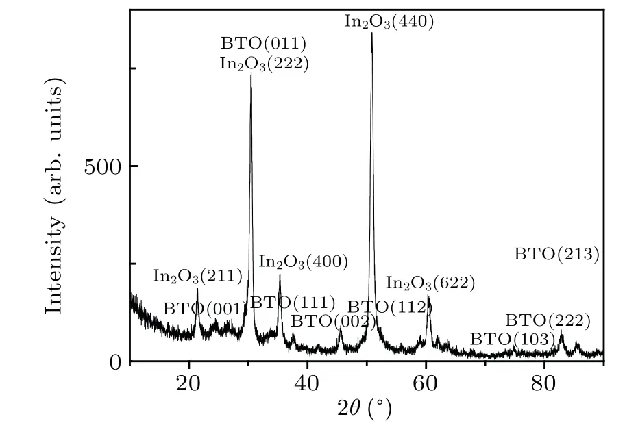
Fig.1. XRD pattern of BITO film.
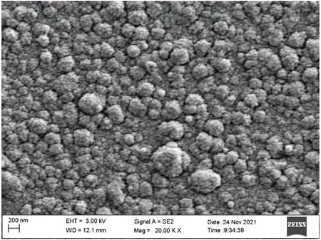
Fig.2. The surface morphology of BITO film.
The transmittance and reflectance spectra of BITO film on glass substrate from wavelength of 300 nm to 2000 nm are shown in Fig. 3. The overall transmittance of the film is in 70%–85% in the wavelength range of 550 nm–800 nm. The overall reflectance of the film is below 35%in the whole wavelength range. The transmittance and reflectance vary not apparently in the near infrared wavelength range due to the low electron carrier concentration in film as listed below. The absorption of film is calculated byA=1-T-R,which sharply decreases from 300 nm indicating the absorption edge is at approximately 300 nm for the cut-off property at ultraviolet wavelength of transparent conductive film. The carrier electron concentration in film at RT tested by Hall system is 1.6×1019cm-3, which is larger than the effective density of states (4×1018cm-3) in conduction band at RT. This causes electrons fulfill at the low energy levels in conduction band and photons with energy larger than the intrinsic band gap be absorbed. The absorption decreases to zero above 600 nm.

Fig.3. The transmittance and reflectance spectra of BITO film.
The linear refractive index (N1), extinction coefficients(K)and film thickness of BITO are measured by SE method.The film has thickness of 300 nm. TheN1andKare shown in Fig.4(a). The real and imaginary components of the dielectric constantsε1andε2are calculated by (N1+iK)2=ε1+iε2,as shown in Fig.4(b). Figure 4(c)shows the cole–cole plots,from which the high frequency dielectric constantε∞is determined at the interception of the real axis. The absorption coefficientαis calculated byα=4πK/λ,as shown in Fig.4(d).It is known that the exponential optical energy dependence ofαnear the band gap can be described byα∝exp(E/Eu),whereEis the photon energy andEuis the Urbach energy related to the joint density of states determined by both conduction and valence band tail states. The extractedEuis 32 meV.The indirect gap is determined by constructing Tauc plots of(αhν)1/2versus hν. The resulting indirect gap is 2.7 eV, as seen in Fig.4(e).The associated direct gap obtained from Tauc plot with (αhν)2versus hνis found to be 3.2 eV, as shown in Fig. 4(f). The spectral-dependent linear refractive index dispersion can be evaluated by the single effective-oscillator model proposed by Wemple–Didomenico.[13]TheN1of the film can be related with oscillator energy(Eo)and dispersion energy(Ed)by the following equation:

wherehνis the photon energy,EoandEdare single oscillator constants.Eois the average excitation energy for electronic transitions andEdis the dispersion energy which is a measure of the strength of inter-band optical transitions. This model describes the dielectric response for transitions below the optical gap. It plays an important role in determining the behavior ofN1. Figure 4(g) shows the optical dispersion behavior of (-1)-1versus(hν)2for the film. The oscillator parametersEoandEdare determined by fitting a straight line to the points. The slope of the linear relation represents (EoEd)-1and the interception with the vertical axis equalsEo/Ed. The values ofEoandEdare 3.5 and 2.9, respectively. The static refractive indexNscan be determined byNs=(1+Ed/Eo)1/2=1.4.[14]The static dielectric constant(εs)is estimated byεs==1.8. The refractive index can also be analyzed to determine the average oscillator wavelength(λ0)and oscillator length strength(S0)for the film. To obtain these values,the single term Sellmeier oscillator is used as[13]
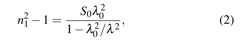
Theλ0andS0values are obtained by the linear parts of 1/(-1)versus λ-2, as shown in Fig. 4(h), whereλ0=375 nm andS0=7.1×10⁻⁶nm-2. It is known that the induced dielectric polarization(P)depends on the applied electrical field(E)which can be expressed in a series of powers ofEby[15]
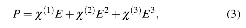
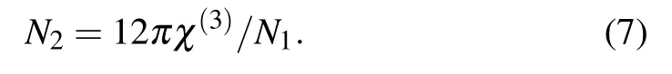
whereχ(1),χ(2), andχ(3)represent the linear, second, and third-order nonlinear optical susceptibilities,respectively. The refractive indexN(λ)can be expressed as
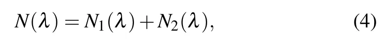
whereN1(λ)andN2(λ)are the linear and nonlinear refractive indexes. Theχ(1)is calculated by
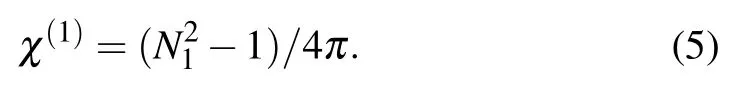
Theχ(3)is calculated by
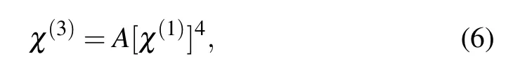
whereAis equal to 1.7×10⁻¹⁰esu. TheN2is calculated by
Theχ(1),χ(3), andN2all follow the same variation trend ofN1(λ)as shown in Figs.4(i)–4(k).
The resistivity (ρ), mobility (μ), and electrical density(n) of the BITO film at RT are studied by Hall apparatus at RT.The van der Pauw technique in a magnetic field of 0.5 T is used to obtain the Hall constantRH. The recorded resistanceR□is related to the resistivityρbyρ=R□dwheredis the film thickness. The conduction mobilityμcan be found byμ=(ρen)-1. The electron density is found fromn=f/eRHwherefis a factor which depends on the type of scattering and the degree of degeneracy in the semiconductor. For complete degeneracy one may putf=1. The sample is n-type withR□=704.7 Ω/□,ρ~0.02 Ω·cm,andμ~18.9 cm2/V·s andn~1.6×1019cm-3.
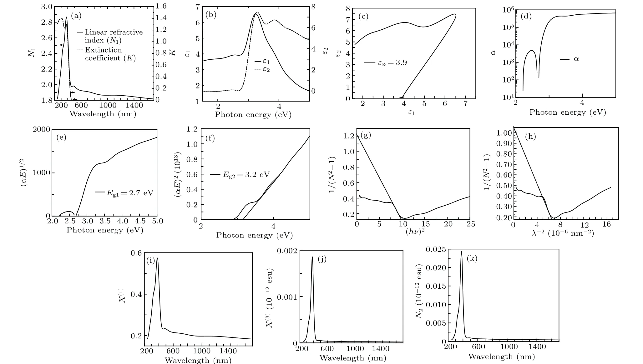
Fig.4. (a) Linear refractive index and extinction coefficient, (b) real and imaginary parts of dielectric constants, (c) cole–cole plot of dielectric constants,(d) absorption coefficient, (e) indirect and (f) direct band gaps, (g) optical dispersion behavior 1/(-1) versus (hν)2, (h) optical dispersion behavior 1/(-1) versus (λ)-2, (i) linear nonlinear optical susceptibility, (j) third order nonlinear optical susceptibility, and (k) nonlinear refractive index of of BITO film.
4. Conclusion and perspectives
The BTO and In2O3mixed film was first deposited by FCVA technique at RT.The structure,basic optical properties,and electrical properties of the film were studied. The film had isolated In2O3and BTO polycrystalline phases,in which the polycrystalline BTO structure was first prepared at RT.The optical and electrical properties studied in this paper suggested that the BITO film fabricated by FCVA was a potential transparent conductor and can be used in low temperature device process. The results also indicated a new depositing technique of FCVA at RT for BTO-based transparent conductive film on glass substrate.
Acknowledgement
Project supported by the Enterprise Science and Technology Correspondent for Guangdong Province,China(Grant No.GDKTP2021015200).

- Chinese Physics B的其它文章
- The coupled deep neural networks for coupling of the Stokes and Darcy–Forchheimer problems
- Anomalous diffusion in branched elliptical structure
- Inhibitory effect induced by fractional Gaussian noise in neuronal system
- Enhancement of electron–positron pairs in combined potential wells with linear chirp frequency
- Enhancement of charging performance of quantum battery via quantum coherence of bath
- Improving the teleportation of quantum Fisher information under non-Markovian environment