MoS2/Si tunnel diodes based on comprehensive transfer technique
Yi Zhu(朱翊), Hongliang Lv(吕红亮),†, Yuming Zhang(张玉明), Ziji Jia(贾紫骥),Jiale Sun(孙佳乐), Zhijun Lyu(吕智军), and Bin Lu(芦宾)
1School of Microelectronics,Xidian University,The State Key Discipline Laboratory of Wide Band Gap Semiconductor Technology,Xi’an 710071,China
2Department of Integrated Circuit Design,Institute of Microelectronics Technology,Xi’an 710071,China
3School of Physics and Information Engineering,Shanxi Normal University,Taiyuan 030031,China
Keywords: 2D/3D heterostructure,transfer technique,tunnel diode,MoS2/Si
1. Introduction
The 2D/3D tunneling field-effect transistors(TFETs)are of great interest in recent years due to their excellent potentials for future ultralow-power applications.[1–3]The 2D/3D TFET combines 3D bulk materials as the source and 2D materials as the channel. Thus,the doping technology restriction in 2D materials,which is a currently dominant constraint for the 2D/2D TFET performance enhancement, can be effectively broken through by the mature and stable doping technology in 3D materials.[2,4]Meanwhile, the pristine interface of the 2D/3D heterostructure due to the dangling-bond-free interface of the 2D material significantly suppresses the trap-assisted tunneling process(TAT)induced by interface traps,which is a Gordian knot of III–V heterojunction TFETs and leads to the relatively high off-state current(IOFF)and subthreshold swing(SS).[5,6]Moreover, the atomically thin channel enhances the electrostatic control over the entire tunneling junction for ultrasteep subthreshold switching.[4]Due to the existence of the van der Waals gap at the interface,the ultrasharp doping profile is available for the 2D/3D tunnel heterostructure, which improves the tunneling efficiency and increases the on-state current (ION).[1,4]The vertically stacked 2D/3D heterostructure is an important guarantee for the realization of the facetunneling mechanism, which greatly increases the effective tunneling area and enhances the gate control over the tunnel junction.[4–6]Therefore,the higherIONand the steeper SS are obtained compared with the traditional point-tunneling mechanism. Consequently,steep subthreshold swing,large on-state current,and small off-state current can be obtained simultaneously in the 2D/3D TFETs.
The tunnel diode based on the 2D/3D heterostructure as a key element for the 2D/3D TFET is necessary to be intensively explored. The transfer technique is currently the most common method to fabricate the heterojunctions based on the 2D materials,which can be generally divided into two categories—mechanical transfer and chemical transfer,according to the different exfoliation processes.[1–4,7–10]The mechanical transfer relies on the mechanical force to lift off the 2D materials from the original growth substrates and release the lift 2D materials onto the 3D bulk material substrates. By this method,only a small part of the irregular films can be usually lifted off and transferred onto the target substrates. The small and uncontrollable film area limits the large-scale fabrication of the 2D/3D heterojunction diodes.[1–4,7]The chemical transfer process leverages the etching of the original growth substrates by the hazardous chemical etchants to exfoliate the 2D materials and release the lift films onto the target substrates. The poly(methyl methacrylate) (PMMA) is generally spin-coated on top of the 2D material to act as the protective barrier and help deal with the ultrathin 2D material film. However, the deformation of the PMMA/2D material assembly is greatly common in the transfer process due to the soft nature of the assembly, leading to the presence of the observable wrinkles and the stacks in the 2D material.[9,10]The performance of the 2D/3D heterojunction is possibly affected by the nonuniformity of the film. In addition,the new growth substrates are in demand to support the growth of the high-quality 2D materials for the next transfer process due to the dissolution of the growth substrates by chemical agents during the lift off,which greatly increases the manufacturing cost.[8–10]Moreover, the quality of the 2D materials is possibly affected by the ions in the etchant solution,which is a main factor of the degradation of the 2D/3D heterojunction performance.[8–10]Therefore, a comprehensive transfer technique that can mend up the shortages of the main methods mentioned above without hurting the benefits is still in urgent need for the development of the 2D/3D tunnel diodes.
In this paper, a low-cost transfer technique that can simultaneously realize a complete lift off and release of the uniform 2D material films and eliminate the degradation of the 2D material quality due to the ions in the chemical etchants is proposed. The MoS2/Si 2D/3D tunnel diodes are experimentally demonstrated by the method we presented. Furthermore,the relatively high crystal quality of the transferred monolayer MoS2films stacked on the Si substrates is confirmed by atomic force microscopy(AFM),scanning electron microscopy(SEM),and Raman characterizations,followed by the evaluation of the electrical characteristics. The prominent negative differential resistance(NDR)effect is observed at room temperature, which can be attributable to the energy band alignments between the N--doped MoS2films and the P+-doped Si substrates. The bilayer MoS2/Si tunnel diode is also fabricated by repeating the transfer process we proposed,followed by a further analysis of the electrical properties. Additionally, the impact of the MoS2film bulk resistance and the contact resistance on the electrical properties of the tunnel diodes is analyzed and the quality of the MoS2electrical contact is estimated by the transfer length method(TLM)approach.
2. Device structure and fabrication
The schematic device structure of the MoS2/Si 2D/3D tunnel diode is exhibited in Fig.1(a). It is worthwhile to point out that sulfur vacancies are identified as the dominant defects in the MoS2films due to the extremely low formation energy.[11–13]As a result,the MoS2film commonly shows the feature of the n-type semiconductor resulting from the structural defects.[11–13]The P+-doped Si substrate is designed to be located beneath the MoS2film to form the PN junction.The 2D/3D heterostructure composed of dissimilar layers stacked in the vertical direction is the critical building block for the future fabricated 2D/3D face-tunneling FET.
The basic steps of the process flow for the MoS2/Si 2D/3D tunnel diode are shown in Fig.1(b).The Si(100)wafer with the doping concentration of 1×1020cm-3is firstly prepared. After defining the isolation region by photolithography, the trenches are formed by the standard silicon etching process. SiO2is subsequently deposited by plasma-enhanced chemical vapor deposition (PECVD), followed by chemical mechanical polishing (CMP) to expose the silicon surface.The monolayer MoS2is immediately transferred onto the Si substrate as soon as the oxide on the Si surface is etched,which is an important guarantee for the high-quality MoS2/Si tunnel junction. Further details of the transfer process will be noted in the next paragraph. The MoS2region patterning is conducted by ion beam etching (IBE). Finally, the Ni/Ti/Au metal electrodes are sequentially formed by lithography,electron beam evaporation and lift-off process. Figure 1(c) also gives the optical microscope image of the fabricated MoS2/Si tunnel diode.

Fig.1. (a)Schematic cross-sectional view of the MoS2/Si 2D/3D tunnel diode. (b)Process flow for the fabrication of MoS2/Si 2D/3D tunnel diode. (c)Optical microscope image of the fabricated MoS2/Si 2D/3D tunnel diode.

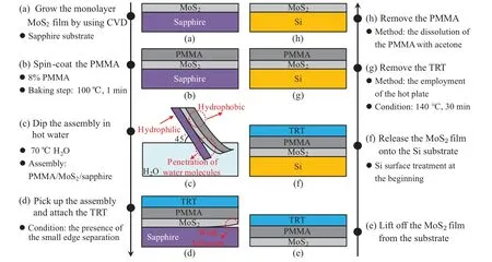
Fig.2. The details of the transfer process to lift off the monolayer MoS2 and release the film onto the Si substrate.
The transfer process is schematically exhibited in Fig.2.The monolayer MoS2is synthesized on the sapphire substrate by using chemical vapor deposition (CVD), which is a common choice for the high-quality MoS2film.[10,14]The PMMA is spin-coated on top of the monolayer MoS2film and baked at 100°C for 1 min. The PMMA/MoS2/sapphire assembly is subsequently dipped in hot water(~70°C)at a feeding angle of 45°with respect to the water surface. It has been demonstrated that the PMMA and the MoS2film are hydrophobic,[15]while the sapphire substrate is hydrophilic.[16]Therefore, the water molecules can easily penetrate underneath the monolayer MoS2film, which significantly weakens the adhesion between the sapphire substrate and the MoS2film. An angle of 45°is also designed to enhance the water penetration efficiency. As the small edge separation between the MoS2and the sapphire substrate is observed,the PMMA/MoS2/sapphire assembly is taken out of the water. A thermal release tape(TRT) that acts as the supported membrane is then attached firmly on the PMMA.Next,the complete TRT/PMMA/MoS2assembly can be lifted off from the sapphire substrate and instantly transferred onto the Si substrate. After that,the transferred assembly is baked on the hot plate (~140°C) for 30 min to remove the TRT and strengthen the attachment between the monolayer MoS2and the Si substrate.[1]The final step of the transfer process is dissolving the PMMA with acetone.[17]
The transfer technique we proposed is generally applicable for the vast majority of the 2D materials. This is because most of the 2D materials, such as TMDs[15]and graphene,[18]are hydrophobic. In contrast, the single crystalline sapphire is hydrophilic,which is a commonly selected substrate for the growth of the 2D materials due to its atomically smooth surface.[8,19]As a result, the penetration of the water molecules between the 2D materials and the sapphire substrates can be universally employed to weaken the adhesion at the interface,followed by the complete exfoliation process with the help of a TRT. Since the TRT functions as the supporting layer,the deformation of the PMMA/MoS2assembly due to its soft nature is significantly mitigated during the transfer process. The transferred film retains its uniformity and thus,the degradation of the 2D/3D heterostructure performance caused by the wrinkles and the stacks of the 2D material film can be eliminated to a large degree. Moreover, the transfer process minimizes the mechanical force with the aid of the water and the TRT and the complete 2D material films[Fig. 3(a)] instead of the small irregular films can be transferred onto the target substrates. Thus, the limitation on the large-scale fabrication of the 2D/3D tunnel diodes and TFETs can be overcome by means of the transfer technique we proposed. Furthermore,as an etchant-free transfer technique,the original growth substrates will not be etched by chemical solutions and can be recycled and reused to grow the high-quality 2D materials. Thus, a lower manufacturing cost can be obtained. Meanwhile,the degradation of the 2D material quality due to the ions in the chemical etchants can be eliminated and the 2D/3D heterojunction can keep its pristine state, which is an important guarantee for the performance of the 2D/3D diodes and TFETs.
3. Results and discussion
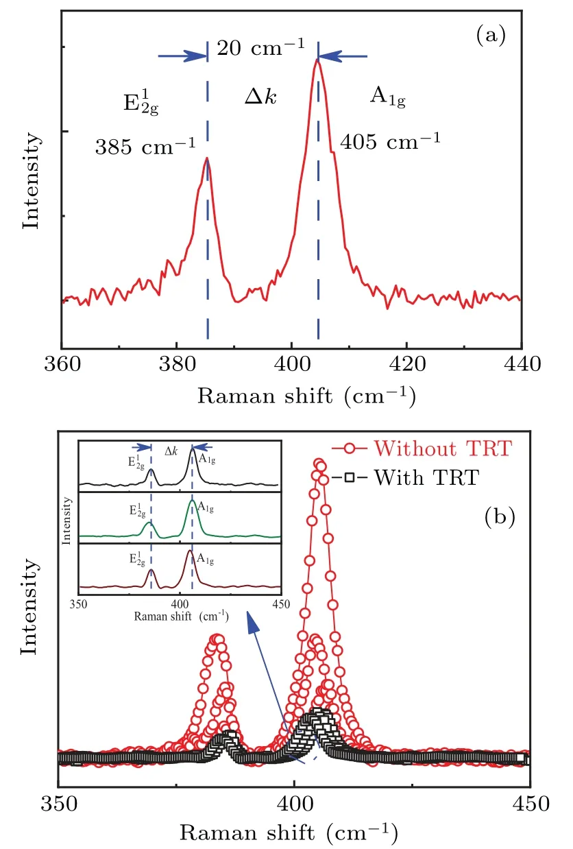
The thickness of the MoS2film is around 0.7 nm confirmed by AFM measurement [Fig. 3(b)] before the transfer process, which indicates the fact that the synthesized MoS2film is a monolayer.[20]A SEM image of the sample after the transferred MoS2film patterning is given in Fig.3(c). In contrast to the visible damages arising from the traditional transfer technique,[1,4]the film transferred by the method we proposed appears to be very smooth and clean with no observable cracks, wrinkles and voids. Figure 4(a) is the Raman spectra collected from the transferred MoS2film. There are two characteristic peaks (and A1g) located at 385 cm-1and 405 cm-1, respectively, corresponding to what was previously reported for the monolayer MoS2.[21]Moreover, the frequency difference Δkbetween the two peaks is around 20 cm-1, which is consistent with the feature of monolayer MoS2, further demonstrating the fact that the MoS2film remains a monolayer after the transfer process.[21]Additionally,the full-width at half-maximum (FWHM) of thepeak,which is considered as an indicator to evaluate the crystal quality, is around 5.3 cm-1. The similar result compared with what has already been reported[22]suggests that the transferred monolayer MoS2remains relatively high crystalline quality.The Raman characterization of the three points randomly selected in the transferred monolayer MoS2film(black square)is shown in Fig. 4(b). The similar Raman spectra of the selected points (details shown in the inset) are observed in the rocking curves,which exhibits the uniformity of the film after the transfer process. This is because the deformation of the PMMA/MoS2assembly is significantly mitigated with the aid of the TRT in the transfer process and thus, the wrinkles and the stacks can rarely exist in the MoS2film. In contrast, the deformation of the assembly leads to the nonuniformity of the transferred film under the condition in the absence of the supported membrane(TRT).As a result,the signal intensity of the three points randomly chosen in the transferred MoS2film is irregularly greater (red circle), indicating the presence of the wrinkles and the stacks in the film[22]that may result in the degradation of the MoS2/Si heterojunction performance.

Fig.3. (a) Optical images of the sample before (top) and after (bottom) the transfer process. (b) AFM image of the MoS2 film before the transfer process. (c)SEM image of the sample after the MoS2 film patterning.

Fig.4. (a)Raman spectra of the transferred MoS2 film. (b)Raman characterization of the three points randomly selected in the MoS2 film with(black square)and without(red circle)the aid of the TRT after the transfer process.The inset shows the detailed Raman spectra of the chosen points in the MoS2 film(black square)after the TRT-assisted transfer process.
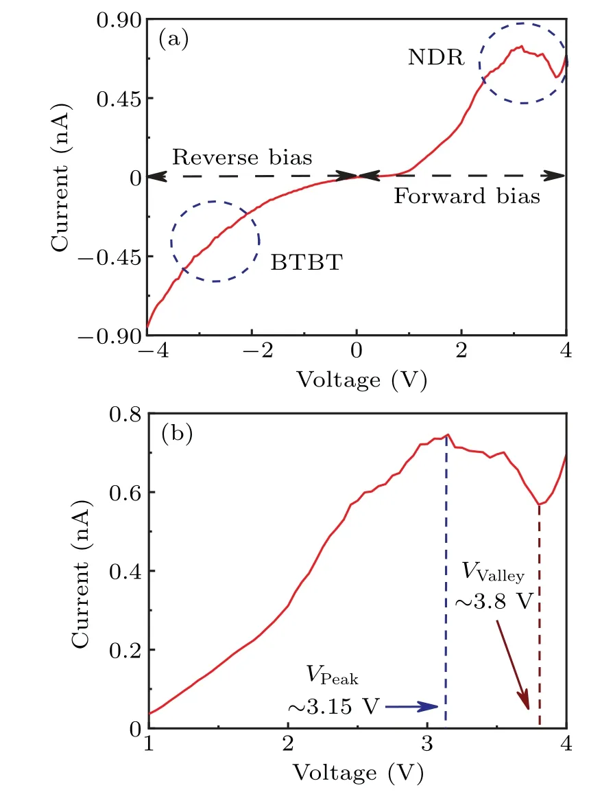
The electrical characteristics of the fabricated tunnel diode is shown in Fig. 5(a). Figure 5(b) gives the zoomed-in view of the electrical characteristics in the forward bias region.When the tunnel diode is biased in the reverse region,the Zenner tunneling current across the MoS2/Si heterostructure dominates and accordingly increases with the voltage bias, consistent with what was previously reported.[20]As the tunnel diode is biased in the forward region,the obvious NDR effect[Fig.5(b)]is observed at room temperature,which is a characteristic feature of the band-to-band tunneling(BTBT)in tunnel diodes.[1,4,14,20]The peak voltage (Vpeak) and the valley voltage (Vvalley) are around 3.15 V and 3.8 V, respectively, and the peak-to-valley current ratio (Ipeak/Ivalley) of the diode is around 1.31,which is higher than that in the reported MoS2/Si and SnS2/Si tunnel diodes.[4,14]
Figure 6(a)illustrates the electrical characteristics of the three different monolayer MoS2/Si tunnel diodes randomly chosen in the wafer. For a more intuitive comparison,the key parameters[4,14,20](includingVpeak,Vvalley,Ipeak/Ivalleyand the tunneling currentIatV=-1 V) are extracted from theI–Vcharacteristics, as shown in Fig.6(b). The almost unchanged electrical properties and key parameters of the different diodes suggest the stable performance of the fabricated tunnel diodes.The stability of the device performance selected randomly further indicates the relatively good quality of the entire bonding interface between the transferred MoS2film and the Si wafer,[4,23]which benefits from the uniform and smooth transferred MoS2films without observable breakage confirmed by the specific analysis above.

Fig.5. (a)The electrical characteristics of the fabricated tunnel diode.(b)The zoomed-in view of the I–V curve in the forward bias region(the obvious NDR effect).
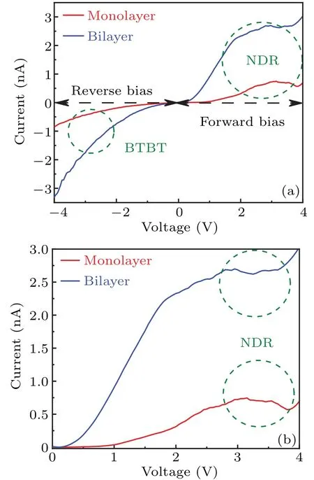
The bilayer MoS2/Si tunnel diode is also demonstrated experimentally. It should be noted that the bilayer MoS2film used to fabricate the diode is formed by repeating the transfer process we proposed and the rest of the experimental procedures are the same as those in the fabrication of the monolayer MoS2/Si tunnel diode. The electrical properties of the monolayer and bilayer MoS2/Si tunnel diodes are shown in Fig.7(a).Figure 7(b)exhibits the zoomed-in view of the forward bias region. Importantly, the NDR effect, which is demonstrated as an indicator for the BTBT mechanism,[4,14,20]is also clearly observed in theI–Vcurve of the bilayer MoS2/Si tunnel diode(blue line). Thus, the bilayer MoS2/Si heterostructure fabricated by the transfer process we proposed also displays relatively excellent performance. In addition,the bilayer MoS2/Si tunnel diode obtains a greater current compared with the monolayer device. The increase of the current can be mainly attributed to the larger cross-sectional area of the MoS2film resulting from the thicker bilayer film.[24]The specific analysis will be given in the last part of this section. Moreover,the peak-to-valley current ratio of the bilayer MoS2/Si tunnel diode(~1.15)is almost unchanged compared with that of the monolayer device (~1.3), consistent with what was previously reported.[20]According to the discussion above, the MoS2/Si tunnel diode with relatively excellent performance and controllable layer number of the film is fabricated by the transfer technique we proposed.

Fig.6.(a)The electrical characteristics of the three different monolayer tunnel diodes selected in the wafer. (b) The key parameters extracted from the current–voltage characteristics.

Fig.7. (a) The electrical characteristics of the monolayer and bilayer MoS2/Si tunnel diodes. (b) The zoomed-in view of the I–V curves in the forward bias region.
The prominent NDR behavior of the tunnel diode can be illustrated by the energy band diagrams in detail. When the reverse bias is applied,the conduction band of MoS2is pulled down and a conductive channel opens (red arrow), allowing the electrons in the Si to tunnel into the MoS2as shown in Fig. 8(a). Thus, the current is dictated by the BTBT mechanism and exponentially increases with the voltage. When the forward bias is applied,the conduction band of MoS2is pulled up and a finite tunneling window exists for the electrons in the conduction band of MoS2to tunnel into the corresponding empty states in the valence band of Si,as shown in Fig.8(b).The tunneling current reaches its peak when the amount of the corresponding available states on the Si side reaches its maximum. Meanwhile, the influence of the reduction in the tunneling window is gradually dominant and the quantity of the corresponding available states on the P+-doped Si side accordingly decreases. As a result, the tunneling current starts to drop. When the applied voltage increases, the conduction band of MoS2is lifted above the valence band of Si and the electrons on the MoS2side can no longer tunnel into the Si side, as shown in Fig. 8(c). With the further increase of the voltage bias, the charge carriers are able to be thermally injected over the low energy barrier between the MoS2and the Si, as indicated in Fig. 8(d). The current begins to be dominated by the thermionic current and increases with the voltage again. In summary,the change of the current with the forward bias gives rise to the NDR behaviour.

Fig.8. Energy diagrams of the MoS2/Si heterojunction at different bias conditions. (a)Reverse bias;(b)small forward bias;(c)forward bias with the suppressed BTBT;(d)large forward bias.
As shown in Fig. 5(a), the current of the fabricated MoS2/Si tunnel diode is not sufficient(~nA).This is because the relatively large series resistance composed of the MoS2film bulk resistance and the contact resistance between the metal and the MoS2exists in the fabricated MoS2/Si tunnel diode. From Ohm’s law for a semiconductor, the bulk resistance is inversely proportional to the cross-sectional area of the MoS2film.[24]The smaller the cross-sectional area,the larger the bulk resistance.[24]The extremely thin MoS2thickness of 0.7 nm leads to the small cross-sectional area of the film and thus, the bulk resistance is large. In addition, the Fermi-level pinning(PLF)at metal/MoS2interface significantly degrades the quality of the MoS2electrical contact[25,26]and the contact resistance is up to 4.175×10⁵Ω·μm measured by the TLM approach.[27–29]Considering the voltage-division effect of the large series resistance,only a fraction of the voltage bias drops across the MoS2/Si heterojunction and thus, an insufficient current is obtained in the fabricated MoS2/Si tunnel diode. In the future work, the transfer technique we proposed can be employed to stack the monolayer high-quality MoS2films and the lower bulk resistance is obtainable arising from the thicker film. Besides,the nickel-etched-graphene electrodes[30]or the ultra-high vacuum metal deposition[31]can be adopted to further reduce the contact resistance.
4. Conclusion
In this article, a low-cost and etchant-free transfer technique is proposed for the large-scale fabrication of the highquality 2D/3D diodes, which mends up the shortages of the common transfer approaches. The MoS2/Si 2D/3D tunnel diode is fabricated based on the method we proposed and the transferred monolayer MoS2film with relatively high crystal quality is confirmed by AFM,SEM,and Raman measurements. Additionally,the prominent NDR effect demonstrated as a characteristic feature of the BTBT in tunnel diodes is observed at room temperature, which verifies the relatively high quality of the MoS2/Si tunnel heterojunction.The bilayer MoS2/Si tunnel diode is also fabricated by repeating the transfer process we proposed. With the exception of the obvious NDR behavior benefiting from the good bonding heterojunction interface,the greater tunneling current is obtained due to the smaller bulk resistance. Finally, the impact of the MoS2film bulk resistance and the contact resistance on the electrical properties of the tunnel diodes is analyzed and the quality of the MoS2electrical contact is estimated by the TLM approach.This study shows the advantages of the transfer technique we proposed and indicates the great application foreground of the fabricated 2D/3D heterostructure for ultralow-power tunneling devices.
Acknowledgement
Project supported by the National Natural Science Foundation of China(Grant No.61851405).
- Chinese Physics B的其它文章
- The coupled deep neural networks for coupling of the Stokes and Darcy–Forchheimer problems
- Anomalous diffusion in branched elliptical structure
- Inhibitory effect induced by fractional Gaussian noise in neuronal system
- Enhancement of electron–positron pairs in combined potential wells with linear chirp frequency
- Enhancement of charging performance of quantum battery via quantum coherence of bath
- Improving the teleportation of quantum Fisher information under non-Markovian environment

