
Multifunctional silicene/CeO2 heterojunctions: Desirable electronic material and promising water-splitting photocatalyst
2022-09-16 05:24LingXuJinZengQunLiXinLuoTongChenJingjingLiuLingLingWng
Chinese Chemical Letters 2022年8期
Ling Xu, Jin Zeng, Qun Li, Xin Luo, Tong Chen,, Jingjing Liu,Ling-Ling Wng
a Energy Materials Computing Center, School of Energy and Mechanical Engineering, Jiangxi University of Science and Technology, Nanchang 330013, China
b Department of Applied Physics, School of Science, East China Jiaotong University, Nanchang 330013, China
c Key Laboratory for Micro-Nano Optoelectronic Devices of Ministry of Education, School of Physics and Electronics, Hunan University, Changsha 410082,China
ABSTRACT The first-principles calculations demonstrate that covalently bonded (cb) heterojunction and van der Waals (vdW) heterojunction can coexist in silicene/CeO2 heterojunctions, due to the different stacking patterns.Especially, the cb heterojunction with band gap of 1.97 eV, forms a type-II heterojunction, exhibits good redox performance and has high-effective optical absorption spectra, thus it is a promising photocatalyst for overall water splitting.Besides, for the vdW heterojunction, the Dirac cone of silicene is well kept on CeO2 semiconducting substrate, with a considerable energy gap of 0.43 eV, which can be an ideal material in building silicene-based electronic device.These results may open a new gateway in both of nanoelectronic device and energy conversion for silicene/CeO2 nanocomposites.
Keywords:Silicene CeO2 Photocatalyst Interfacial interaction Dirac cone
In recent decades, lots of studies have devoted themselves to searching high-performance photocatalysts to split water into clean energy hydrogen (H2) [1–5].Stimulated by the graphene boom,a large number of two-dimensional (2D) catalytic materials have been studied [6–13].As an element of the same group as C, Si is an important carrier in the electronic semiconductor industry.And its two-dimensional morphological structure, named silicene (the silicon counterpart of graphene but with a slightly buckling of about 0.44) also has been theoretically investigated and experimentally synthesized [14–18].Silicene shares many of the intriguing electronic properties in graphene, such as Dirac cone, high Fermi velocity and carrier mobility [19–22].Considering the advantages of being inherently compatible with ubiquitous silicon-based semiconductor technology and facile tunability of the energy gap, in addition to constructing microelectronic devices, it may even be a good candidate for photocatalytic materials.The key lies in how to effectively adjust its band gap to obtain good photocatalytic performance, or opening without destroying its inherent Dirac Fermion characteristics for next-generation electronic-device application.
With the successional synthesis of various non-toxic and cheap nanostructured CeO2, rational design of nano-CeO2supporting substrates or CeO2-based nanocomposites are considered as a prominent approach to realize better reaction activities and catalytic performance [23–29].The rapid formation and elimination of oxygen vacancies in CeO2, such as the reversible phase transition between CeO2and Ce2O3, endow it with high oxygen storage capacity and chemical activity, which plays an important role in the catalytic oxidation reactivity of the cerium oxide surface [30,31].Inspired by the significantly enhanced performance in our previous work of SiH/CeO2heterojunction [32] and graphene/CeO2heterojunction [26].We consider combining silicene with CeO2bulk material to form silicene/CeO2heterojunctions is very likely to obtain more intriguing properties than the two individuals, and even than graphene/CeO2heterojunction.In this paper, based on stateof-the-art hybrid density functional theory (the calculation details are in Supporting information), clearly studing the electronic properties of bulk Si/CeO2and silicene/CeO2heterojunctions.Our works not only find a superior semiconducting substrate material to grow or integrate Si/silicene, but also provide a promising visible-light photocatalyst for hydrogen production, or a promising electronicdevice.
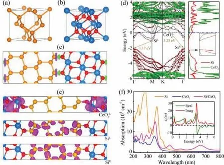
Fig.1.The unit cell of (a) Si in a diamond cubic crystal structure and (b) CeO2 in a fluorite structure.(c) The geometric structure and 3D charge density difference of Si/CeO2 nanocomposite with an isovalue of 0.001 e/3.Green and purple isosurfaces represent charge accumulation and depletion, respectively.(d) Band structures (left panel) and PDOS (right panel) of Si/CeO2 heterojunction.The red circles and green squares in the left panel denote the projection to Si and CeO2 constituents, respectively.(e) The electronic density distribution of CeO2L, SiL and SiH, with an isovalue of 0.02 e/3.(f) The absorption spectra of Si, CeO2 and Si/CeO2 heterojunction, and the inset denotes the calculated dielectric function of Si/CeO2 heterojunction, including both real and imaginary parts.Red, yellow, and blue spheres represent O,Si, and Ce atoms, respectively.
We firstly explore the Si/CeO2heterojunctions.As shown in Figs.1a and b, Si and CeO2nanocrystals are both cubic crystal structures and share an approximate bulk lattice constant a, which is 5.43and 5.41[33,34], respectively, and the lattice constants of their (111) surfaces are even closer, as given in Table S1(Supporting information).Therefore, a 1 × 1 stoichiometric cubic CeO2(111) surface slab with 9 layers is used to match an approximate 1 × 1 supercell for Si(111) plane with 8 layers, realizing a negligible lattice mismatch of only 0.16% in their nanocomposite,the details are listed in Table S1.Our calculations clearly demonstrate that the Si/CeO2nanocomposite is a covalently bonded (cb)heterojunction with a typical cb equilibrium spacing of 1.69(Fig.1c).And the inapparent electron transfer at interface further confirms the formation of covalently-linked interface in Si/CeO2heterojunction.Although the Si/CeO2heterojunction is a gapless metal, there may be a sizable optical band gap for Si/CeO2heterojunction (Fig.1d).The band width between the lowest unoccupied molecular orbital (LUMO) and highest occupied molecular orbital (HOMO) corresponding to the isolated Si (SiLand SiH) is 1.17 eV, this value exactly equals to the band gap of isolated bulk Si [33], as illustrated in Fig.S1b (Supporting information).Meanwhile, the band width between LUMO of CeO2and the HOMO of Si (CeO2Land SiH) is 3.23 eV, and this value approximates to the energy gap of freestanding CeO2nanocrystals (Fig.S2b and c in Supporting information) [35].The electronic density distributions of CeO2L, SiLand SiHhave been plotted in Fig.1e, which confirms our observations and analyses.Subsequently, the optical absorption spectra of Si/CeO2heterojunction and its constituents are given in Fig.1f.Si/CeO2composite shows a similar absorption curve with that of CeO2, except that the former is much stronger especially in the long wave region of visible light.In addition, to further verify our calculations, the electronic structure and optical properties of isolated Si, Si(111), CeO2, CeO2(111) are also given (Figs.S1 and S2 in Supporting information), and these results are found to be in excellent agreement with others [33–38].Although Si/CeO2heterojunction is not a promising photocatalyst, its optical band gap is very interesting and remains to be explored.
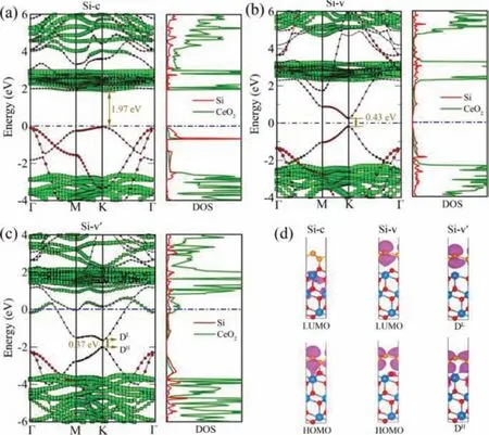
Fig.2.Projected band structures (left panel) and PDOS (right panel) for (a) Si-c, (b)Si-v, (c) Si-v’.Their side views of HOMO and LUMO with an isovalue of 0.02 e/3 are given in (d).The red circles and green squares in the left panels represent the projection to CeO2(111) and silicene constituents, respectively.The Fermi level is set to zero.
Combining CeO2with Si to form Si/CeO2heterojunction cannot significantly improve the photocatalytic performance of CeO2, so we turn to explore the silicene/CeO2heterojunctions.Our previous work has proved that the silicane (SiH)/CeO2is a type-II heterojunction with excellent photocatalytic performance [32].The geometric and electronic structures of silicene and silicane are quite different.Silicene and silicane are both low buckled structures with a buckling height of 0.43 and 0.73, and their Si-Si bond lengths are 2.25 and 2.34, which are consistent with the results of previous studies [15,32,39].Silicene is a gapless semiconductor that is not a good candidate as photocatalyst (Fig.S3 in Supporting information) [40], and it can be further proved by the inferior visible-light absorption of silicene (Figs.S3d and e).Due to the lattice constants of silicene and CeO2(111) are very close (Table S1) [15,41].Hence, we select a 1 × 1 silicene unit on the surface of 1 × 1 CeO2(111) supercell to obtain a lattice mismatch in their composites as low as 0.30%.For the silicene/CeO2heterojunctions, there are five different stacking patterns with various atom-alignment types, among which, two are cb heterojunctions and three are vdW heterojunctions (Fig.S4 in Supporting information).Based on the value of adhesive energies (Ead) (Table S1), the leftmost configuration in Fig.S4 (Si-c), and the rightmost configuration in Fig.S4 (Si-v) are selected as the representatives of cb heterojunctions and vdW heterojunctions, respectively.Subsequently,the molecular dynamics simulation and phonon dispersions further confirm their stability (Fig.S5 in Supporting information).In addition, whether the conversion between Si-v and Si-c is easy is also a question worth considering.Using CINEB method, we calculate the energy profiles and structures of the transition states for Si-v to Si-c.As shown in Fig.S6 (Supporting information), the energy barrier from Si-v to Si-c is as high as 2.626 eV, indicating that this process is not easy to occur, and also that they have relatively good structural stability.To have a strict and complete study,another case that Ce atoms locate on the outside surface also should be considered, named CeO2(111)’.After structural optimization, the silicene/CeO2(111)’heterojunction with the lowestEadis selected for research (Fig.S7 in Supporting information, named Si-v’).
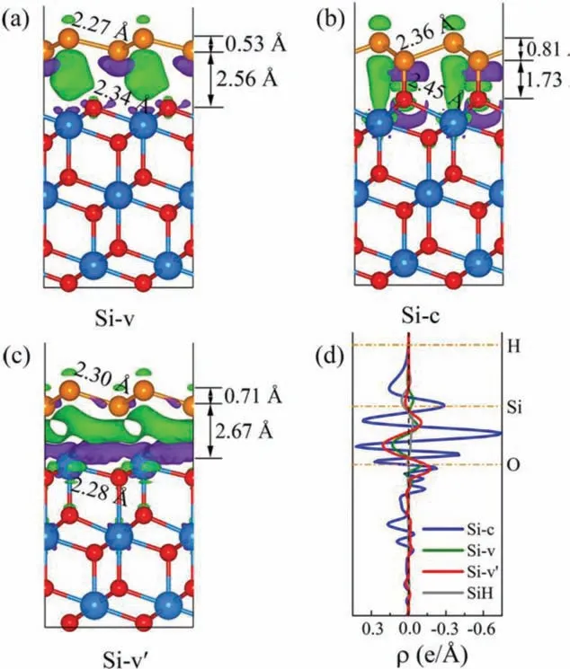
Fig.3.Three-dimensional charge density difference for the (a) Si-v, (b) Si-c and (c)Si-v’.The purple and cyan iso-surfaces denote charge accumulation and depletion in the space, respectively.The horizontal dash dot lines denote the central location of each atomic layer.(d) Profile of the planar averaged charge density difference as a function of positions in the z-direction.The positive and negative values of ρ denote the charge accumulation and depletion, respectively.
As shown in Figs.2a and d, Si-c forms type-II heterojunction with a moderate energy gap of 1.97 eV.Its valence band maximum (VBM) and conduction band minimum (CBM) are dominated by two different individuals, which further confirms the formation of type-II heterojunction, and is very conducive to the separation of photogenerated carriers.More interesting, the Dirac cone of silicene is well kept in Si-v with a dream energy gap up to 0.43 eV,which can pave the avenue for the application of silicene-based high-speed nanoelectronics [42,43].There is no doubt that we have opened a considerable band gap in silicene without damaging its intrinsic electronic structure by combining with CeO2nanocrystal(Figs.2b and d).Additionally, the Si-v’is a metal but displays a similar electronic structure with that of Si-v (Fig.2c).For the Si-v’,there is one point we should note, the Dirac cone of silicene also has been opened, but its Fermi level shifts up and makes this system a gapless metal.Fig.S8 (Supporting information) shows the band structure of silicene with lattice mismatch of 0.3%, and its Dirac cone is still not opened.Therefore, such a small lattice mismatch hardly affects the band structure of silicene.For the pure silicene, the difference of onsite energy between the two sublattices is zero [44].While in the formed Si-v heterojunction, this balance is broken by the interaction between silicene and substrate CeO2.This point can also be confirmed from the charge analysis.We can see the charge density difference (Fig.3a), due to the effect of the substrate CeO2, the charges of the two Si atoms in the silicene layer are obviously different.Bader calculations show that the upper and lower Si atoms gain 0.0360 e and lose 0.0540 e, respectively.This can be attributed to the formation of the built-in electric field in the interlayer, also proves that the potential balance between the two Si atoms in the silicene layer is no longer maintained, the symmetry between the two sublattices of silicene is broken and the two Si atoms are no longer identical [44], so the Dirac cone is captured in Si-v.And the Dirac cone is captured in Si-v’for the same reason, the upper and lower Si atoms lose 0.0004 e and gain 0.3750 e, respectively.Of course, for the Si-c,the formation of Si-O destroys the inherent electronic structure of silicene, so Dirac cones cannot be captured and has undergone major changes.

Fig.4.(a) The optical absorption spectra of CeO2(111) and silicene individuals, as well as Si-c, Si-v heterojunctions.(b) The comparison of absorption spectra for CeO2(111)’ and Si-v’, and the inset denotes the calculated dielectric function of Si/CeO2 heterojunction, including both real and imaginary parts.(c) Calculated VBM and CBM potentials versus normal hydrogen electrode of CeO2(111), silicene, Si-c,and Si-v.The upper and lower red dashed lines stand for the proton reduction potential (H+/H2) and oxygen reduction potential (O2/H2O) for water splitting with values of 0 and 1.23 eV, respectively.(d) Schematic diagram of photocatalytic water splitting for Si-c, as well as the electron transfer during the photocatalytic process.
Among the three heterojunctions, Si-c exhibits the most effective optical absorption and Si-v owns the widest response range in the whole UV-vis light (Fig.4a).By comparing with the constituents, we can see that the optical absorption of Si-c has been enhanced greatly.Besides, the optical absorption spectra of Si-v’and the CeO2(111)’also have been plotted (Fig.4b).Although Si-v’is a gapless metal, it demonstrates a significantly improved UV-vis absorption, especially around the UV ray, which implies its promising application in the field of photocatalytic.In addition, to shed light on the potential applications of these heterojunctions in producing hydrogen, their band edge potentials with respect to the water redox potentials have been aligned in Fig.4c.To be an eligible photocatalyst in hydrogen production, the band gap of them must cross the redox potential of water splitting [45–47].Clearly,neither the silicene nor Si-v is an adequate photocatalyst for water splitting, because they do not have strong enough redox properties (blue block in Fig.4c).But the CeO2and Si-c can do well in water splitting.Moreover, Si-c is a type-II heterojunction with suitable band gap, which is benefit to the effective separation of photo-excited electrons and holes.On the basis of above results and analyses, we can conclude that the Si-c is very likely to be an excellent water-splitting photocatalyst (Fig.4d).
Furthermore, to have an insight into the interfacial interactions and the enhanced photocatalytic performance of Si-c, their 3D charge density difference and quantitative results of charge distribution are given in Fig.3.One thing to note here is that all the isovalues in Figs.3a and c and Fig.S4 are 0.001 e/3, while that of Fig.3b is 0.005 e/3.The more accurate Bader calculation results are listed in Table S1.Si-c has significantly more charge transfer from silicene to CeO2than Si-v, due to the strong action of Si-O.But silicene in Si-v’gains electrons from CeO2, which should be attributed to the exposed metal Ce atoms on the surface of CeO2.These results can well in line with the analysis of charge density difference.Such a good charge transfer effect of Si-c can more fully demonstrate its remarkable photocatalytic water splitting performance.On the other hand, the transfer of a large amount of charge to CeO2accelerates the reversible phase transition between CeO2and Ce2O3, which to a certain extent provides greater possibilities for the enhancement of the redox properties for CeO2.To further prove it, the charge changes of Ce atoms in the pure CeO2and Si-c are calculated.Results show that the charge of Ce atoms in Si-c is 0.0799 e/atom more than Ce atoms in pure CeO2, indicating that the valence state of Ce atoms in Si-c is reduced, and a reversible phase transition between CeO2and Ce2O3has occurred.
In summary, using first-principles calculations, we systematically investigate the electronic, interfacial and optical properties of Si/CeO2and silicene/CeO2heterojunctions.The Si/CeO2nanocomposite is neither a good photocatalyst nor electronic material due to its unsuitable band structure, but its light absorption performance is well interesting and worthy of further exploration.Interestingly, the silicene/CeO2(111) heterojunctions can stably exist in the forms of both vdW and cb heterojunctions.The Si-c,as a type-II heterojunction with a moderate band gap of 1.97 eV,is an excellent photocatalyst in splitting water to produce hydrogen.In Si-v, the Dirac cone of silicene is well kept and opened up to 0.43 eV, this sizable energy gap over 0.4 eV without degrading its intrinsic Dirac Fermion characteristics is of great significance in silicene-based high-speed nanoelectronics.In short,this paper provides sufficient evidence supporting for designing high-performance silicene-based electronic device and CeO2-based water-splitting photocatalyst.
Declaration of competing interest
The authors report no declarations of interest.
Acknowledgments
This work was financially supported by the National Natural Science Foundation of China (Nos.11764018, 20212BAB201013,31760157), the Jiangxi Provincial Natural Science Foundation(Nos.20202ACBL211004, 20212BAB201013, 20202BABL211009,20192BAB212003) and the Science and Technology Planning Project of Ganzhou City.
Supplementary materials
Supplementary material associated with this article can be found, in the online version, at doi:10.1016/j.cclet.2021.11.026.
 Chinese Chemical Letters2022年8期
- Chinese Chemical Letters的其它文章
- Adsorptive removal of PPCPs from aqueous solution using carbon-based composites: A review
- A review on hollow fiber membrane module towards high separation efficiency: Process modeling in fouling perspective
- Recent advances in DNA glycosylase assays
- Chiral pillar[n]arenes: Conformation inversion, material preparation and applications
- Recent progress in carbon-based materials boosting electrochemical water splitting
- Working principle and application of photocatalytic optical fibers for the degradation and conversion of gaseous pollutants