
Single- and few-layer 2H-SnS2 and 4H-SnS2 nanosheets for high-performance photodetection
2022-06-20 08:00LinWangXinzheLiChengjiePeiCongWeiJieDaiXiaoHuangHaiLi
Chinese Chemical Letters 2022年5期
Lin Wang, Xinzhe Li, Chengjie Pei, Cong Wei, Jie Dai, Xiao Huang, Hai Li
Key Laboratory of Flexible Electronic (KLOFE) & Institute of Advanced Materials (IAM), Nanjing Tech University, Nanjing 211816, China
Keywords:Tin disulfide 2H and 4H phases Phase-dependent behavior Ultralow-frequency Raman spectroscopy Photodetection
ABSTRACT The properties of two-dimensional (2D) materials are highly dependent on their phase and thickness.Various phases exist in tin disulfide (SnS2), resulting in promising electronic and optical properties.Hence,accurately identifying the phase and thickness of SnS2 nanosheets is prior to their optoelectronic applications.Herein, layered 2H-SnS2 and 4H-SnS2 crystals were grown by chemical vapor transportation and the crystalline phase of SnS2 was characterized by X-ray diffraction, ultralow frequency (ULF) Raman spectroscopy and high-resolution transmission electron microscope.As-grown crystals were mechanically exfoliated to single- and few-layer nanosheets, which were investigated by optical microscopy, atomic force microscopy and ULF Raman spectroscopy.Although the 2H-SnS2 and 4H-SnS2 nanosheets have similar optical contrast on SiO2/Si substrates, their ULF Raman spectra obviously show different shear and breathing modes, which are highly dependent on their phases and thicknesses.Interestingly, the SnS2 nanosheets have shown phase-dependent electrical properties.The 4H-SnS2 nanosheet shows a current on/off ratio of 2.58 × 10⁵ and excellent photosensitivity, which are much higher than those of the 2HSnS2 nanosheet.Our work not only offers an accurate method for identifying single- and few-layer SnS2 nanosheets with different phases, but also paves the way for the application of SnS2 nanosheets in highperformance optoelectronic devices.
Because of the suitable band gap, excellent carrier transport and good light stability, the layered tin disulfide (SnS2) crystals exhibit extensive applications in the fields of battery, photocatalyst, photodetector, gas sensor and field-effect transistor [1–13].In layered SnS2crystal, Sn atoms octahedrally coordinate with the S atoms to form S-Sn-S layer.Typically, the 1T’, 2H and 3R phases are found in layered transition metal dichalcogenides (TMDCs).It is known that the properties and performance of layered materials are highly dependent on their phase and thickness [14,15].For instance, the metallic 1T’-MoS2shows excellent catalytic performance while the monolayer 2H-MoS2is a semiconductor with direct bandgap [16,17].Therefore, accurate phase and thickness identification is very important to the practical application.Different from layered TMDCs, it has been reported that several tens of polytypes exist in SnS2crystals due to the different stacking sequence, such as 2H, 4H, 18R.Among them, the 2H-SnS2and 4HSnS2have been widely investigated due to their excellent properties in the applications of optoelectronic and flexible electronic devices [1,18–21].However, accurate identification of 2H-SnS2or 4H-SnS2nanosheet is still a challenge due to the lack of suitable identification technique.Therefore, it is an essential prerequisite to identify the phase and thickness of SnS2nanosheets before extending their promising applications.
Raman spectroscopy has been considered as a convenient and nondestructive technique to distinguish the phase of 2H-SnS2and 4H-SnS2bulk crystals [22].Both 2H-SnS2and 4H-SnS2nanosheets show characteristic peak located around 315 cm-1[23,24].In addition, two weak E-mode peaks located at 200 cm-1and 214 cm-1are the characteristic peaks for 4H-SnS2crystal.While for 2H-SnS2crystal, there is a weakEgmode located at 205 cm-1, which is different from the 4H-SnS2[23].However, the E-mode andEgpeaks are too weak to be measured in monolayer and few-layer 2H-SnS2and 4H-SnS2nanosheets.Therefore, it is difficult to distinguish 2HSnS2and 4H-SnS2nanosheets by measuring high-frequency Raman spectrum.
As a powerful and nondestructive technique, ultralow frequency(ULF) Raman spectroscopy has attracted much attention for accurate thickness and phase identification of 2D TMDCs nanosheets in recent years [25,26].The ULF Raman spectra of 2D TMDCs and graphene are fingerprints for identifying their thicknesses and phases [27].It has been reported that the bilayer and few-layer 2H-MoS2and 3R-MoS2nanosheets can be easily distinguished by their ULF Raman spectra [26].Moreover, single-layer to more than ten-layer 2H-MoS2and 2H-WSe2nanosheets can be identified from their ULF Raman spectra [25].The 4H-SnS2crystal shows an ULF shear mode peak around 27 cm-1while 2H-SnS2crystal has no ULF Raman signal at 77 K.Although the ULF Raman spectra of single- and few-layer 2H-SnS2nanosheets have been reported [24], the ULF Raman spectra of single- and few-layer 4HSnS2nanosheets are largely unexplored.Moreover, the photodetection ability of 2H-SnS2and 4H-SnS2nanosheets is also seldom investigated in detail.
In this work, the 2H-SnS2and 4H-SnS2crystals were successfully prepared by chemical vapor transport (CVT) method.The 2H and 4H polytype structures were confirmed by X-ray diffraction (XRD), ULF Raman spectroscopy and high-resolution transmission electron microscope (HR-TEM) measurements.After singleand few-layer 2H-SnS2and 4H-SnS2nanosheets were deposited on 90 nm SiO2/Si substrates, optical microscopy (OM), atomic force microscopy (AFM) and ULF Raman spectroscopy were used to characterize them.The thickness-dependent optical contrast plots and ULF Raman spectra of single- to ten-layer 2H-SnS2and 4H-SnS2nanosheets were well established to facilitate the accurate thickness and phase identification.In addition, the electrical properties of 2H-SnS2and 4H-SnS2nanosheets were also measured to investigate their optoelectronic performance.The 4H-SnS2nanosheet shows an on/off current ratio of 2.58 × 10⁵, which is three orders of magnitude higher than that of the 2H-SnS2nanosheet.In addition, the photosensitivity of 4H-SnS2nanosheet is around two orders of magnitude higher than that of 2H-SnS2nanosheet, indicating the 4H-SnS2has much better optoelectronic performance than 2H-SnS2.Our work can not only offer an accurate method for identifying SnS2nanosheets with different polytypes and thicknesses,but also demonstrate a promising candidate for high-performance optoelectronic device.
Synthesis of SnS2crystals:The growth of SnS2single crystals by CVT method was carried out in a closed quartz tube.High-purity tin (3 mm, 99.99%, Aladdin) and sulfur powders (99.95%, Aladdin)with a molar ratio of 1:2 were placed at one end of the quartz tube as the source zone, while the other end of the quartz tube was the growth zone.The distance between the source zone and the growth zone is 14.5 cm.After the quartz tube was sealed with oxyhydrogen flame at 10-5Torr, it was placed into a double-heating zone tube furnace.The source and growth zones were maintained at 900 °C and 880 °C for 7 days, respectively.The average rate of increase and decrease of temperature was approximately 5 °C/min.Thus, the 4H-SnS2crystal was obtained.
Similarly, after the sealed quartz tube with high-purity tin and sulfur powders was placed into a double-heating zone tube furnace, the source and growth zones were maintained at 580 °C and 560 °C for 7 days, respectively.After that, the 2H-SnS2crystal was obtained.
Mechanical exfoliation of SnS2nanosheets:The 2H-SnS2and 4H-SnS2crystals were mechanically exfoliated into monolayer and few-layer nanosheets on 90 nm SiO2/Si substrates.
Characterizations:The phase-structural composition of SnS2single crystal was investigated by X-ray diffraction using a Rigaku SmartLab diffractometer (Cu-radiation) at scanning speed of 10°/min in the 2θrange of 5°-85° The detailed atomic structure of SnS2nanosheets was further investigated by HR-TEM (JEOL JEM-2100F, Japan) operated at an accelerating voltage of 200 kV.Optical microscope (ECLIPSE LV100ND, Nikon) was used to initially identify thin SnS2nanosheets.AFM (Dimension ICON with Nanoscope V controller, Bruker) equipped with a scanner (90 × 90 μm2) was used to measure the thickness of exfoliated SnS2nanosheets in tapping mode.The number of layers as well as polytypes of SnS2nanosheets were further confirmed by ULF Raman spectroscopy,which was carried out on a Raman spectrometer (LabRAM HR Evolution, Horiba Jobin Yvon) with a 532 nm laser focused through a 100 × objective lens.The Raman band of a Si wafer at 520.8 cm-1was used as a reference to calibrate the spectrometer.
Device fabrication and photodetection:50 nm thick gold(99.99%, Zhong Nuo New Material Technology Co., Ltd.) and 10 nm thick chromium (99.99%, Zhong Nuo New Material Technology Co.,Ltd.) films were deposited on SnS2nanosheets by using TEM grid(300 meshes) as mask in thermal evaporator.
A probe station (model TTPX, Lake Shore Inc.) and Keithley 4200 semiconductor characterization system were used to monitor the real-time current change of as-prepared devices.The photodetection test was recorded under blue (405 nm), green (532 nm)and red (633 nm) lasers.The power of laser was measured with a laser power meter (Laser power meter LP1, SanWa).
For 2H-SnS2and 4H-SnS2crystals, the covalently bonded S-Sn-S sandwich layers have different stacking sequence along the c axis, as shown in Fig.S1 (Supporting information).Previous report suggested that low-temperature synthesis produces the 2HSnS2, while the crystal grown above 800 °C shows the 4H polytype [23].As shown in Fig.1a, the as-grown 4H-SnS2crystal is yellow and the 2H-SnS2crystal is brown with size of 3–4 mm.The crystalline structure of 2H-SnS2and 4H-SnS2crystals was firstly explored by XRD (Fig.1b).The XRD pattern of 2H-SnS2crystal grown at 580 °C shows obvious diffraction peaks at 15.06°, 28.15°,30.37°, 32.13°, 41.94°, 46.16°, 50.06°, 52.44°, 60.56° and 63.02°, respectively, which are well consistent with the standard PDF card(JCPDS No.23–0677).The dominant (001) peak indicates that the 2H-SnS2single crystal grows preferably along this orientation.In addition, the XRD pattern of SnS2crystal grown at 900 °C also confirms the 4H polytype (JCPDS No.89–3198).The strong diffraction peak located at 14.96° can be indexed to the (001) plane of 4HSnS2, while those weaker diffraction peaks at about 29.04°, 46.02°and 49.98° can be indexed to the (002), (003) and (110) planes, respectively, which are consistent with literature [28].Moreover, the ULF Raman spectra of as-grown SnS2crystals also confirm their 2H and 4H polytypes.As shown in Fig.1c, the Raman spectrum of SnS2crystal grown at 900 °C shows two E mode vibration peaks at 198 cm-1and 216 cm-1as well as a strong peak at 315 cm-1in the high frequency region, which are consistent with the Raman peaks of 4H-SnS2crystal [23].Meanwhile, there is a strong peak located at 27 cm-1in the ultralow frequency region (<50 cm-1),further confirming the 4H polytype [29].In terms of SnS2crystal grown at 580 °C, there is a weak peak at 205 cm-1besides a strong peak at 315 cm-1in the high frequency region.Moreover,there is no peak in the ULF region, indicating the structure of 2HSnS2[24].Apart from aforementioned peaks, the A1g-LA (M) mode was also observed both in 2H-SnS2and 4H-SnS2crystals, locating at ~140 cm-1[30].
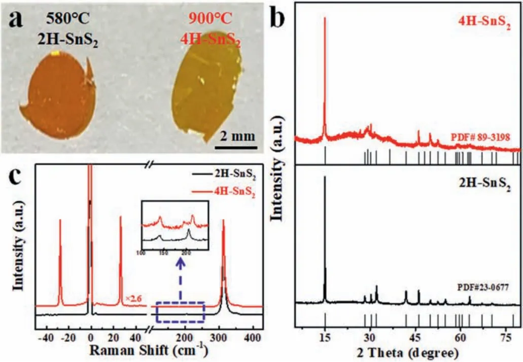
Fig.1.(a) Optical image of 2H-SnS2 and 4H-SnS2 crystals grown at 580 °C and 900 °C.(b) XRD patterns and (c) Raman spectra of 2H-SnS2 and 4H-SnS2 crystals.
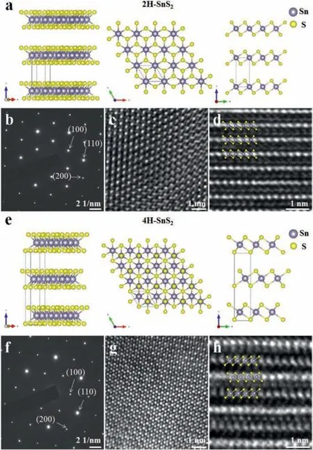
Fig.2.Simulated structures of the (a) 2H-SnS2 and (e) 4H-SnS2 crystals.The SAED patterns, top-view and cross-section HR-TEM images of (b–d) 2H-SnS2 and (f-h) 4HSnS2.
In order to further understand the detailed structure of assynthesized SnS2crystals, their atomic arrangement was characterized by HR-TEM and selected area electron diffraction (SAED)pattern, as shown in Figs.2a–h.The simulated atomic arrangements of Sn and S atoms in 2H-SnS2and 4H-SnS2are shown in Figs.2a and e, respectively.It is known that the 2H-SnS2and 4HSnS2crystals have trigonal prismatic and octahedral coordination.High-quality single crystal structure without other diffraction spots and diffraction rings was clearly indicated by the SAED patterns of 2H-SnS2and 4H-SnS2, as shown in Figs.2b and f.Diffracted spots of the SAED pattern were recognized as (100), (200) and(110) planes, indicating the well-defined layered structure oriented along the (001) plane of SnS2[31].The 4H-SnS2has four sulfur layers in one unit cell (Figs.2e and h, Fig.S1), and two Sn atom layers are situated between the two nearest-neighbor S atom layers, respectively.However, the 2H-SnS2has two sulfur layers in one unit cell (Figs.2a and d, Fig.S1), and the Sn atom layer locates at bilevel S atom layers [28].Due to the larger atomic number than S atoms, the brighter atoms are identified as Sn atoms, as shown in Figs.2c, d, g and h.Therefore, the HR-TEM images clearly revealed the trigonal and hexagonal arrangements of the atoms in 2H-SnS2and 4H-SnS2crystals.According to the side-view HR-TEM images of 2H-SnS2and 4H-SnS2, the well-defined sandwich-like layered structures were visually presented.The HR-TEM results are consistent with the XRD patterns, which further confirmed that the SnS2crystals grown at 580 °C and 900 °C were assigned to 2H-SnS2and 4H-SnS2, respectively.
Similar to other TMDCs materials, the thickness of SnS2nanosheets can be easily and reliably determined by measuring the optical contrast [25,32,33].As shown in Fig.S2 (Supporting information), 1–10 L 2H-SnS2and 4H-SnS2nanosheets were deposited on 90 nm SiO2/Si substrates.The monolayer 2H-SnS2and 4H-SnS2nanosheets are difficult to be found due to their weak contrast on 90 nm SiO2/Si substrate.As the thickness of 2H-SnS2and 4H-SnS2nanosheets increases, the optical contrast in blue channel increases while that in red channel decreases (Figs.3a–d).Moreover, the 2HSnS2and 4H-SnS2nanosheets have almost same optical contrast in blue channel (Fig.3c).The AFM characterizations indicate that the 1 L to 10 L 2H-SnS2and 4H-SnS2nanosheets also show similar thickness (Figs.S3 and S4 in Supporting information).Thus, it is difficult to distinguish them by using AFM and optical contrast in blue channel.The 1-3 L 2H-SnS2and 4H-SnS2nanosheets have similar optical contrast in red channel (Fig.3d).While the 4-10 L 2H-SnS2and 4H-SnS2nanosheets show different optical contrast in red channel, which could be used to distinguish them.In addition,the 1-10 L 2H-SnS2and 4H-SnS2nanosheets show quite different optical contrast in green channel, which can also be used to distinguish them.For 1 L to 5 L 4H-SnS2nanosheets, the optical contrast in green channel is negative.It turns to positive when the thickness of 4H-SnS2exceeds 6 L.While for 2H-SnS2nanosheet, the optical contrast in green channel turns to positive once its thickness exceeds 4 L.As shown in Figs.3e, f, i and j, the 4 L 2H-SnS2and 4H-SnS2nanosheets show similar color and height in OM and AFM images.After the green channel images are extracted from their color OM images (Figs.3g, h, k and l), it is clear that the 4 L 2H-SnS2nanosheet has an optical contrast of 4 while that of 4 L 4H-SnS2nanosheet is -8.Thus, the 4 L 2H-SnS2and 4H-SnS2nanosheets can be easily distinguished by measuring their optical contrast in green channel.
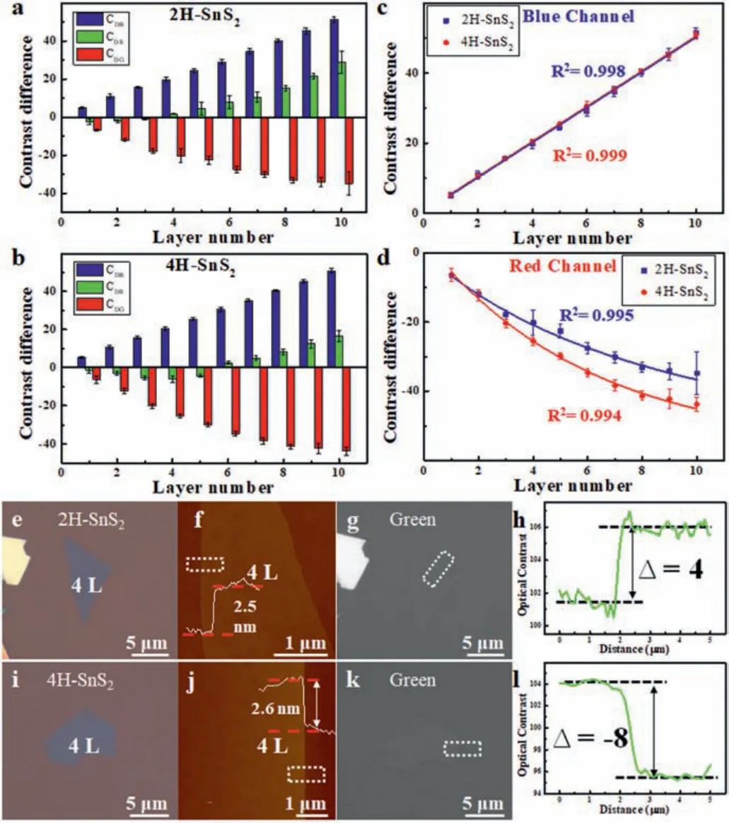
Fig.3.Plots of optical contrast of 1–10 L (a) 2H-SnS2 and (b) 4H-SnS2 nanosheets in red (CDR), green (CDG), and blue (CDB) channels on 90 nm SiO2/Si substrates.Plots of (c) CDB and (d) CDR values of 1–10 L 2H-SnS2 and 4H-SnS2 nanosheets on 90 nm SiO2/Si substrates.Optical microscopy, AFM topography, grayscale green channel images, and the corresponding contrast profiles of 4 L (e–h) 2H-SnS2 and (i–l) 4H-SnS2 nanosheets on 90 nm SiO2/Si substrates, respectively.
It is well known that the ULF Raman spectroscopy can be used to identify the stacking sequence (i.e., crystal phase) and thickness of atomically-thin 2D materials [25,29].Previously, monolayer and few-layer 2H-SnS2nanosheets have been characterized by ULF Raman spectroscopy [24].The thickness-dependent ULF shear and breathing modes were observed, which could be used to identify the thickness of 2H-SnS2nanosheets.Although the ULF Raman spectrum of 4H-SnS2crystal has been reported in 1980s [29],that of 4H-SnS2nanosheet has not been explored.As shown in Figs.4a and b, the ULF breathing (B) and shear (S) mode peaks of 1–10 L 2H and 4H-SnS2nanosheets are measured.Fig.4a shows the ULF Raman spectra of 1 L to 10 L 2H-SnS2.The 2 L 2H-SnS2nanosheet has only one S peak (S1) at the position of 18.3 cm-1.With the increase of thickness, the S1 peak gradually red-shifted from 2 L (18.3 cm-1) to 6 L (7.1 cm-1).The S1 peak is beyond the measurement range of our instrument for 7 L to 10 L 2H-SnS2nanosheets.When the thickness increases to 3 L, a new breathing mode (B1) was observed.The B1 peak gradually red-shifted from 3 L (21.8 cm-1) to 10 L (7.3 cm-1).Since a new B2 peak appears, there are three peaks in the ULF Raman spectrum of 6 L 2H-SnS2nanosheet, which is different from other layers.With the increasing thickness, the B2 peak gradually red-shifted from 6 L(18.8 cm-1) to 10 L (11.2 cm-1).The shear and breathing mode peaks of 2H-SnS2gradually red-shift as the thickness increases.However, with the increasing thickness of 4H-SnS2nanosheets, the S1 peak gradually blue-shifts while the B1 peak gradually redshifts.These phenomena are similar to those of 2H-MoS2and 2H-WSe2nanosheets [25].As shown in Fig.4b, monolayer 4HSnS2nanosheet has no peak in the ULF region, while 2 L 4HSnS2nanosheet has only one S peak at the position of 19.3 cm-1.The S peak gradually blue-shifted from 2 L (19.3 cm-1) to 10 L(26.7 cm-1).For 3 L 4H-SnS2, the B and S might be mixed together to show a broad peak, which is similar to that of 3 L 2HMoS2[24].When the thickness increased to 4 L, a weak breathing mode was observed.The B1 peak of 5 L 4H-SnS2becomes obvious and gradually red-shifts as the thickness increased to 10 L.The shear and breathing mode peaks can be distinguished by using polarized Raman measurement, as shown in Fig.S5 (Supporting information).Figs.4c and d show the evolution of ULF shear and breathing modes as a function of the thickness of 4H-SnS2and 2HSnS2nanosheets.Since the Raman shifts of high-frequency Raman peaks of SnS2nanosheets are insensitive to the layer numbers (Fig.S6 in Supporting Information), their ULF Raman peaks can be fingerprint for accurately determining not only the thickness but also the phase of monolayer and few-layer 2H-SnS2as well as 4H-SnS2.
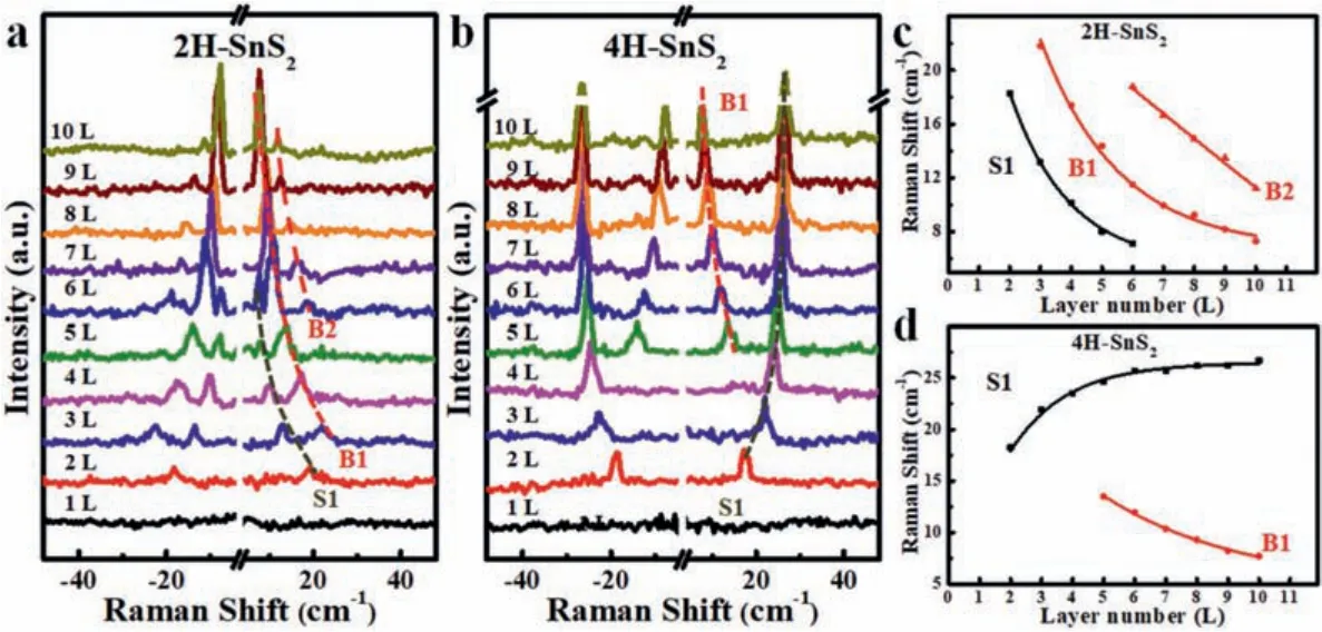
Fig.4.ULF Raman spectra of 1–10 L (a) 2H-SnS2 and (b) 4H-SnS2 nanosheets.Peak position as a function of layer number of 1–10 L (c) 2H-SnS2 and (d) 4H-SnS2 nanosheets.
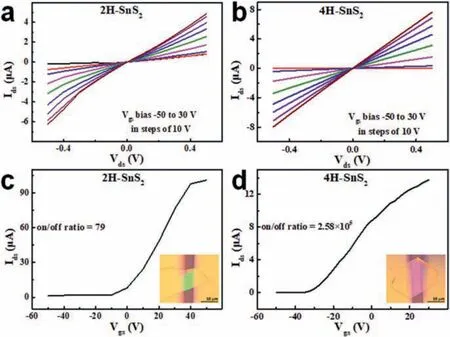
Fig.5. Id-Vd curves of (a) 2H-SnS2 and (b) 4H-SnS2 at Vg ranging from -50 V to 30 V. Id-Vg curves of (c) 2H-SnS2 and (d) 4H-SnS2 at bias of 0.5 V.
To further explore their electrical properties, 2H-SnS2and 4HSnS2nanosheets-based field effect transistors (FETs) were fabricated.As shown in Figs.5a and b, both 2H-SnS2and 4H-SnS2nanosheets based devices show linear and symmetricId-Vdcurves when the gate voltage increases gradually from -50 V to 30 V,indicating good Ohmic contact between the Cr/Au electrodes and SnS2nanosheets.The transfer characteristic curves of FET devices based on 2H-SnS2and 4H-SnS2indicate that they are n-type semiconductors (Figs.5c and d).The mobility andIon/Ioffratio were measured to demonstrate the performance of 2H-SnS2and 4HSnS2FETs.When the bias is 0.5 V, theIonandIoffof 2H-SnS2device were 100.8 nA and 1.27 nA, and theIon/Ioffratio is 79.However, theIonandIoffof 4H-SnS2device were 13.75 μA and 53.3 pA at the same bias, and thus theIon/Ioffratio is 2.58 × 10⁵.The mobility is 1.61 cm2V-1s-1for 2H-SnS2FET device.While the 4HSnS2FET device has a mobility of 12.95 cm2V-1s-1.Aforementioned results suggest that 4H-SnS2nanosheet shows much better electrical performance than 2H-SnS2nanosheet.Following the electrical measurement, the photodetection performance of 2HSnS2and 4H-SnS2devices was investigated under the 405, 532 and 633 nm lasers with different incident power density, respectively.The photocurrents of 2H-SnS2and 4H-SnS2were dependent on the incident power density.Photosensitivity is usually described by the ratio of photocurrent to dark current (PDR) [34–37], which is used to evaluate the performance of optoelectronic device and defined as:

whereIphotois the photocurrent under illumination, andIdarkis the baseline current without illumination.
The photodetection performance of 2H-SnS2and 4H-SnS2nanosheets under lasers with different wavelength and power density was shown in Figs.6a–c and Figs.S7 and S8 (Supporting information), respectively.The photodetectors based on 2H-SnS2and 4H-SnS2nanosheets exhibited quite stable characteristics after multiple illumination-dark cycles.Fig.6a shows the photosensitivity of 2H-SnS2and 4H-SnS2photodetectors under 405 nm laser with a power density of 3.52 mW/mm2.The corresponding PDRs of 2H-SnS2and 4H-SnS2are about 87 and 3165, respectively.Meanwhile, the PDRs of 4H-SnS2are about 856 and 664 under 532 nm(power density of 0.56 mW/mm2) and 633 nm (power density of 8.46 mW/mm2) lasers.The corresponding PDRs of 2H-SnS2are about 25 and 15 at the same condition, respectively, as shown in Figs.6b and c.The PDR of 4H-SnS2photodetector is several tens of times higher than that of the photodetector based on 2H-SnS2,indicating the excellent photosensitivity of 4H-SnS2photodetector.As shown in Fig.S8 (Supporting information), both the 2H-SnS2and 4H-SnS2photodetectors have good photoresponse to the 405,532 and 633 nm lasers with various power densities.The photosensitivity declines with the decreased power density of the incident light, indicating the photocurrent has a strong dependence on the laser power density.Under the fixed bias, a larger laser power density will lead to an increase of photo-induced carrier, resulting in larger photocurrent.As show in Figs.6d–f, the PDRs of 2HSnS2and 4H-SnS2were plotted as a function of the power density under various lasers.By fitting the data, theIphoto/Idarkcan be expressed by a power-law equationIphoto/Idark∝Pα, wherePis the laser power intensity andαis an exponent.The linear relationship with a power dependence of ~1 existed in 4H-SnS2, indicating that the absorbed photons can be effectively transformed into photoinduced carriers during laser illumination [8,38].However, the sublinear relationship with a power dependence less than 1 existed in 2H-SnS2, indicating defects and charge impurities may be filled by photoexcited carriers, which result in photocurrent saturation through recombination losses as the laser intensity increased [8].This phenomenon has also been observed in other layered material-based photodetectors [39,40].The time-resolved photoresponse of the 2H-SnS2and 4H-SnS2photodetectors wereillustrated in Fig.S9 (Supporting information), in which a rising time (Tr) of 1.13 s and a decay time (Td) of 2.96 s were measured in 4H-SnS2photodetector under 405 nm laser at a power density of 3.52 mW/mm2.Meanwhile,Trof 1.31 s andTdof 1.97 s were obtained for 2H-SnS2photodetector.Moreover, the 4H-SnS2and 2HSnS2photodetectors can fastly respond to 532 and 633 nm lasers with power density of 0.56 mW/mm2and 8.46 mW/mm2, respectively.Furthermore, we also studied the photoresponsivity (R) of 4H-SnS2and 2H-SnS2by the following equation,
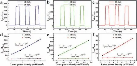
Fig.6.(a–c) The photocurrent-to-dark-current ratios (PDRs) of photodetectors based on 2H-SnS2 and 4H-SnS2 nanosheets under 405, 532 and 633 nm lasers with power density of 3.52 mW/mm2, 0.56 mW/mm2 and 8.46 mW/mm2, respectively.(d–f) Plots of the PDRs of photodetectors based on 2H-SnS2 and 4H-SnS2 nanosheets at 405, 532 and 633 nm lasers as a function of laser power density.

whereIphis the photocurrent,Pis the incident light intensity,andSis the effective illuminated area.Interestingly, the photoresponsivity of 4H-SnS2photodetector is up to 2.18 × 10⁵mA/W(P= 3.52 mW/mm2), which is about an order of magnitude higher than that of 2H-SnS2photodetector (4.32 × 10⁴mA/W).The promising performance of 4H-SnS2is compared with previous works and listed in Table 1 [1,5,7,8,21,41–43].The aforementioned results illustrate that 4H-SnS2shows much better optoelectronic performance than 2H-SnS2, implying the influence of crystalline phase on the performance.
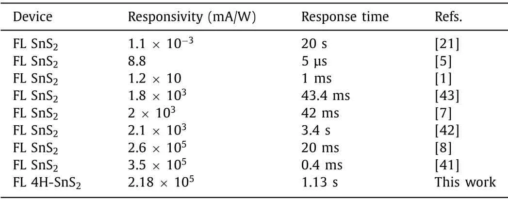
Table 1 Comparison of the photodetector performance based on few-layer (FL) SnS2 nanosheets.
In summary, 2H-SnS2and 4H-SnS2crystals have been successfully synthesized by CVT method.The as-synthesized 2HSnS2and 4H-SnS2have been distinguished by XRD, ULF Raman spectroscopy, and HR-TEM.The ULF shear and breathing Raman modes of 2H-SnS2and 4H-SnS2nanosheets have been clearly observed, which can be used as fingerprint to identify the thickness and phase of mechanically exfoliated 1 L to 10 L nanosheets.Although the optical contrasts of 1 L to 10 L 2H-SnS2and 4H-SnS2nanosheets in blue channels are indistinguishable,their optical contrasts in red and green channels can be used to identify the thickness.Both of them show n-type behaviors, while 4H-SnS2nanosheet shows much higher on/off current ratio and mobility than 2H-SnS2nanosheet.Impressively, photodetectors based on 4H-SnS2exhibited excellent performance under blue,green and red lasers, which is much higher than that of 2H-SnS2.This work could draw attention to the exploration of SnS2with various phases for their potential applications in optoelectronic devices.
Declaration of competing interest
The authors declare that they have no known competing financial interests or personal relationships that could have appeared to influence the work reported in this paper.
Acknowledgments
This work was supported by the National Natural Science Foundation of China (Nos.51832001, 21571101 and 51322202), the Natural Science Foundation of Jiangsu Province in China (No.BK20161543), and the Natural Science Foundation of the Jiangsu Higher Education Institutions of China (No.15KJB430016).
Supplementary materials
Supplementary material associated with this article can be found, in the online version, at doi:10.1016/j.cclet.2021.09.094.
 Chinese Chemical Letters2022年5期
- Chinese Chemical Letters的其它文章
- Recent advances in enhancing reactive oxygen species based chemodynamic therapy
- An integrative review on the applications of 3D printing in the field of in vitro diagnostics
- Recent developments of droplets-based microfluidics for bacterial analysis
- Dynamics and biological relevance of epigenetic N6-methyladenine DNA modification in eukaryotic cells
- Recent progress in advanced core-shell metal-based catalysts for electrochemical carbon dioxide reduction
- Recent advances in carbon-based materials for electrochemical CO2 reduction reaction