
Stacking driven Raman spectra change of carbon based 2D semiconductor C3N
2022-06-20 08:00YuchengYangWenyaWeiPengHeSiweiYangQinghongYuanGuqiaoDingZhiLiuXiaomingXie
Chinese Chemical Letters 2022年5期
Yucheng Yang, Wenya Wei, Peng He, Siwei Yang,*, Qinghong Yuan,Guqiao Ding,*, Zhi Liu, Xiaoming Xie
a School of Physical Science and Technology, ShanghaiTech University, Shanghai 201210, China
bState Key Laboratory of Functional Materials for Informatics, Shanghai Institute of microsystem and Info rmation Technology, Chinese Academy of Sciences,Shanghai 200050, China
c College of Materials Science and Opto-Electronic Technology, University of Chinese Academy of Sciences, Beijing 100049, China
d State Key Laboratory of Precision Spectroscopy, School of Physics and Electronic Science, Key Laboratory of Polar Materials and Devices (MOE), East China Normal University, Shanghai 200241, China
Keywords:C3N Raman spectrum Carbon based semiconductor 2D materials Stacking structure
ABSTRACT As a two-dimensional carbon based semiconductor, C3N acts as a promising material in many application areas.However, the basic physical properties such as Raman spectrum properties of C3N is still not clear.In this paper, we clarify the Raman spectrum properties of multilayer C3N.Moreover, the stacking driven Raman spectra change of multilayer C3N is also discussed.
C3N with D6h-symmetry is a kind of two-dimensional (2D) carbon based semiconductor [1,2].It has drawn wide attention since reported in 2017 [1].Yanget al.suggested that C3N acts as a promising material in many application areas such as 2D microelectronic devices, magnetic devices, microbiological detection [1].After that, amounts of researches around C3N have been studied theoretically [3,4].Until today, the experimentally synthetical 2D carbon-nitrogen materials can be list as:g-C3N4, C2N-h2D, C3N5and monolayer C3N [1,5-10].The structural information of Raman shifts and IR bands for g-C3N4, C2N-h2D, C3N5, monolayer C3N and graphene were shown in Table S1 (Supporting information)[1,6-10].In terms of the element composition and bonding, all of the carbon-nitrides are composed of conjugated aromatic structure (sp2) bonded by carbon and nitrogen atoms (C=C, C-N, C=N,etc.), leading to approximate spectral peak/band positions.Differing from other carbon-nitrides, nitrogen atoms are in the form of graphite N, inducing distinction derived from abundant C-N bonds.In terms of morphology, C3N is the only hole-free layered material by nature that have been successfully obtained artificially among those 2D layered carbon-nitrides.The uniqueness of hole-free and carbon-predominated C3N makes it more similar to graphene.It is worth noting that, differing from graphene, C3N obtains unique electrical behaviors due to its specific lattice structure [11–16].Wanget al.predicted the carrier mobility tuning of C3N with different stacking structure [11].The band gap tuning of C3N sheets is also predicted by Donget al.[12].These results refer that C3N has many fascinating intrinsic natures, ensuring its significant value in various applying areas (such as microelectronic devices, lithiumion batteries, full cells and memristor) [13–16].
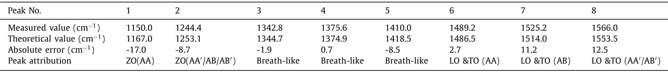
Table 1 Summary of peak signals of theoretical and experimental Raman spectra
Although C3N has been raised as a promising carbon based semiconductor, it is difficult to obtain high qualified sheets experimentally with effective characterizations.It is reported that a C3N-like network structure was claimed to be prepared by the pyrolysis of organic single crystals, hexaaminobenzene trihydrochloride, at 500 °C [17].However, the products seemed to be a bulk structure which is hard to be exfoliated into 2D sheets.Besides,the synthetic process was complex.Yang’s work in 2017 [1] reported a hydrothermal method for synthetic C3N sheets following a bottom-up process.The single-layer or multi-layer C3N sheets were obtained by the polymerization of 2,3-diaminophenazine at 250 °C for 48 h, which was relatively time-consuming.In this work, the ultraviolet irradiation was introduced for the first time.The reaction was operated in room temperature and kept for 60 min to acquire multi-layer C3N with high quality, which notably improved the efficiency and controllability of the synthetic process.In previous reports, microscopic methods such as scanning tunneling microscopy (STM) and transmission electron microscope(TEM) were carried out for confirming the C3N structure [1].However, these methods were limited by their local-detection nature,which cannot reflect the picture of the macroscopic quality.On the other hand, spectroscopic means such as X-ray photoelectron spectroscopy (XPS), infra-red spectrum (IR), nuclear magnetic resonance spectrum (NMR) and X-ray diffraction (XRD) can’t precisely describe the stacking structures of C3N.In order to confirm the quality of as-synthesized C3N as well as have a deep understanding of its physical nature, it is essential to seek a comprehensive characterization method for C3N.
Raman spectrum is most commonly used for the characterization of carbon based materials [18].Herein, systematic Raman spectrum of multilayer C3N was investigated detailly with both theoretical calculation and experimental results.Based on high quality products, we took a detailed Raman spectrum study on C3N’s physical structures.The theoretical calculation was also carried out to explore the phonon spectrum features for different stacking types of C3N.Moreover, some structure defects originating from the synthesis process can also be detected by Raman measurement accurately.
Theoretical calculation was carried out to understand the Raman influence of different stacking types of C3N (Fig.1).Four stacking layered C3N were shown in Fig.1a.For AA and AA′ stacking, the carbon and nitrogen atoms have the nearest neighbors directly above and below them in the neighboring layers.In terms of AA stacking, the adjacent atoms are the same element (namely, ‘C to C’and ‘N to N’along vertical direction).In terms of AA′, it can be viewed as the top layer is shifted byC-C bond length along zigzag direction.Thus no ‘N to N’but ‘C to C’and ‘C to N’exist in AA′.In terms of AB and AB′ stacking, it can be viewed as the top layer is shifted by two and one C-N bond length along armchair direction, respectively.For AB stacking, the directly neighboring atoms along vertical direction are the same element as ‘C to C’and ‘N to N’.For AB′ stacking, no ‘N to N’but ‘C to C’and‘C to N’exist.The calculated relative interlayer formation energy and binding energy by density functional theoretical (DFT) calculation were shown in Table S2 (detailed parameters see in Theoretical methodology of Supporting information), which suggested that AA′ is the most energetically favorable bilayer stacking structure[19].Notably, with such a small energy difference, it is likely that no single stacking will dominate at room temperature [19,20].The theoretical Raman spectral lines and Phonon dispersions of corresponded stacking C3N were shown in Figs.1b and c.The methodology of theoretical calculation based on the 2×2×1 rectangle supercell and the density functional perturbation theory (DFPT)method (see in Theoretical methodology of Supporting information) [21].Theoretical Raman spectral lines were investigated (Fig.1b) from the DFPT study, combining with crystal symmetry and Raman activity to calculate Raman frequency [22].The theoretical spectral lines of AA, AA′, AB and AB′ stacking types can be seen in Table 1.The schematic diagram of vibration vector of LO/TO, ZO and breath-like vibrational modes were shown in Fig.S1 (Supporting information).It is worth noting that the spectral lines of AA stacking type shifted to lower frequencies by 86.3 and 67.1 cm-1for ZO and LO/TO modes, respectively, compared with that of AA′stacking.The red shift is suggested to happen as a result of polarizability decrease.It is known that Raman scattering refers to the scattered light radiated by a dipole induced by polarization in the molecule [23].The strength of the induced polarization (P), scales with the polarizability (α), and the incident electric field (E) are described as:
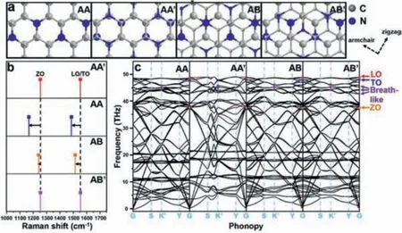
Fig.1.(a) Ball-and-stick models of AA, AA′, AB and AB′ stacking C3N and (b) corresponded Raman spectral lines.(c) Phonon dispersions of AA, AA′, AB and AB′ stacking C3N.

For AA stacking of C3N, due to a larger electronegativity(χN=3.04vs.χC=2.55), each N atom has gained 1.19eelectrons from neighboring C atoms [24].A strong coupling will occur due to the adjacent N atoms directly above and below in the neighboring layers [25].It is assumed that the strong coupling phenomenon may greatly weaken the dispersion of in-plane electron cloud, therefore, decrease the dipolar polarizabilityα.Similar with AA and AA′, a red shift can be observed as well for AB and AB′ (Fig.1b).The red shifts of 13.2 and 40.2 cm-1occurred for ZO and LO/TO modes, respectively.The relative smaller red shifts change compared to that of AA can be ascribed to fewer adjacent N atoms directly above and below in the neighboring layers in AB.The N atom with lone pair electrons as well as larger electronegativity trends to interact with protons by sharing electrons, forming hydrogen bonds [16].With abundant orderly arranged N atoms, layered C3N are can act as a promising filtration membrane in water purification industry [26,27].As shown in Fig.1c, the Raman-responded transverse optical (TO), longitudinal optical (LO),z-direction optical (ZO) and breath-like modes on special points for Brillouin zone integrations are marked, which directly contribute to the Raman signals of C3N [28].It is shown that a slight LO-TO splitting occurs due to molecular polarity of C3N.Besides, three breath-like modes on K’point were also revealed which contributes to breath-like Raman peaks when defective sites formed.The theoretical wavenumber was calculated as 1344.7, 1347.9 and 1418.5 cm-1(Table 1).The breath-like signals come from the breathing modes of six-atom rings and requires a defect for activation, which are originated from an intervalley double resonance process around the K’point in the first Brillouin zone [29–34].
Above theoretical calculation results were further verified by C3N samples from practical synthesis.C3N sheets were preparedviathe ultraviolet (UV) induced graft polymerization method of 2,3-diaminophenazine (DAP).Typically, 25 mg 2,3-diaminophenazine were added into a quartz bottle and diluted by 150 mL absolute ethanol, followed by ultrasonic treatment for 30 min.The solution was transferred into a UV irradiation chamber and irradiated for 60 min.Then the products were separated by centrifugation by 3 times (15000 rpm, 1 h, 15 °C).The element analysis, X-ray photoelectron spectroscopy (XPS), atomic force microscope (AFM) and scanning electron microscope (SEM) were carried out to further conform the structure of the obtained C3N sheets (Table S3, Figs.S2 and S3 in Supporting information).
The lattice structure of C3N was investigated by high resolution transmission electron microscopy (HR-TEM, Fig.S4 in Supporting information).The C3N sheet exhibited a well-ordered lattice morphology with a hole-free structure at a large size of 3500 nm2(Fig.S4a).It is indicated that the polymerization progress of 2,3-diaminophenazine occurred in ordered alongx, ydirections and spontaneously extended to the wholex-yplane, forming a regular periodic crystal arrangement structure with a large size.Fig.S4b shows selected area electron diffraction (SAED) pattern of the(111) plane (diffraction spot diameter was about 60 nm), in which the diffraction pattern of the sample satisfied the ideal hexagonal symmetric structure.The lattice constantsda* anddb* of C3N was 0.432 ± 0.015 nm and 0.249 ± 0.010 nm (a*andb*are corresponding reciprocal unit vectors), respectively.The lattice constants were slightly less than twice of those of graphene (da*=0.213 nm,db*=0.123 nm), which is consistent with the theoretical calculations as reported before [1].
The scanning transmission electron microscopy results (under high-angle annular dark-field mode, HAADF-STEM) of C3N are shown in Fig.2a, which indicated the coexistence of AA′ and AB′stacking types (Fig.2b) within a single C3N sheet.The relative proportion of AA′ and AB′ stacking was 55% and 45%, respectively.Figs.2b and c show the atom-scale images of inner arrangement of Fig.2a.Bold hexagonal honey-comb structure were observed for both AB′ and AA′ stacking with clear distinction due to their different interlayer alignment.The light intensity response curve was furtherly investigated to make a distinction between C and N atoms.As shown in Figs.2d and e, the light intensity changes regularly along the scan line following a 0.244 nm cycle, which accords with the distance between meta atoms within a six-membered ring.The peaks with higher light intensity refer to the participation of N atoms since the atomic number has an effect on light intensity in positive correlation:
Fig.2.(a) Typical HADDF-STEM image of stacking C3N sheet.The area marked purple and green corresponds to AB′ and AA′ stacking C3N, respectively.Enlarged images of (b) AB′ and (c) AA′ stacking C3N.Light response curve of (d) AB′ and (e) AA′stacking C3N.

whereIis the light intensity,Zis the atomic number [35].The ordered high peaks of the curves are well in line with the periodic atom structure of stacking C3N, indicating an efficient graft polymerization progress under UV-irradiation condition.Besides, the AB stacking of C3N was observed shown in Fig.S5 (Supporting information).The absence of AA′ observation can be due to the its relatively lower thermodynamic stability by density functional theoretical calculation (Table S2), which should be at a very small region proportion.Besides, the identification between AA and AA′stacking by electron microscopy technique is difficult because of their structural similarity under observation.
Fig.S6 (Supporting information) shows the powder X-ray diffraction (XRD) spectrum of precursor DAP and product C3N.Significant difference was revealed.For DAP, multiple main peak signals appear in the range of 10°-40°, indicating the XRD complexity of DAP which has aromatic fused rings.The comparison shows that after the polymerization of molecular DAP, the peaks originally located in the range of 10°-40° was indistinguishable.Interestingly, a new crystal diffraction peak appeared at 27.6°, indicating that C3N product has typical crystallographic properties.Furtherly, by Bragg lattice diffraction formula:

the corresponding lattice spacingdof the 2θpeaks is determined to be 0.323 nm.At the same time, by DFT calculation, we derived the theoretical interlayer spacing in different stacking types(Table S4 in Supporting information).The interlayer spacing of as-synthesized C3N is consistent with that of calculated results.As mentioned above, the synthetical 2D carbon-nitrogen materials are g-C3N4, C2N-h2D, C3N5and C3N.The comparison of interlayer spacing for g-C3N4, C2N-h2D, C3N5, C3N and graphene can be derived from Table S4 [19,36-39].Notably, lattice N atoms with a large number within C3N may have an important effect on interlayer spacing.It is known that the interlayer spacing of graphene is 0.335 nm.Comparatively, the interlayer spacing of AA′, AB and AB′ stacking types is smaller, which may be due to the strong interaction between atoms of adjacent layer considering the existence of N atoms.The appearance also applies to other 2D carbonnitrides (Table S4).All the interlayer spacings of other 2D carbonnitrides are ~0.32 nm with only minor differences.Conversely, for AA stacking, the N atoms in the adjacent layers are directly stacked alongzaxis, forming electron-rich centers which might repel each other intensely, so that the interlayer spacing increased slightly compared to that of graphene.The unique characteristics of high degree of N doping in C3N endow it with typical lattice properties,which is different from traditional two-dimensional carbon materials.Furthermore, the uniqueness and diversity of interlayer spacing of stacking types makes C3N a flexible structure applicable to many chemical systems such as intercalation reaction and functional group modification [40,41].
Fig.3a shows practical Raman spectrum of stacking C3N.The ethanol solution of C3N (0.1 mg/mL) was spin-coated (6000 rpm,40 s) on a Silicon substrate.A flake of C3N sheet (lateral size of~2 μm, thickness of 1.9-3.7 nm) was chosen to be detected by a LabRAM-HR spectrometer (Jobin Yvon Co., Ltd., French).Then the sample was treated by annealing at 200 °C (high purity nitrogen, 99.99%) for 2 h in the tube furnace, after which the same region of the C3N sheet was detected.All the Raman collections were performed at room temperature using a 532 nm laser source.The laser power and spot size were 50 mW and 1 μm, respectively.A parallel Raman collection was operated with completely same preparation and characterization approach, which indicated the universality of our dealing process (Fig.S7 in Supporting information).The Raman peaks before annealing are strongly overlapped in the range of 1300-1600 cm-1(gray curve).This typical coherence of Raman shifts indicates the rich structural information of as-synthesized C3N.The Raman peaks narrowed with enhanced Raman peak intensity on the order of 103after annealing.The full width at half maximum (FWHM) of Raman peaks at 1244.4,1342.8, 1375.6, 1410.0, 1489.2 and 1566.0 cm-1were decreased as 18.4, 16.8, 14.4, 19.2, 14.4, 16.8 and 17.6 cm-1, respectively.It is assumed that the high density ordered arrays of C3N after annealing induced a stronger surface plasmon resonance effect due to molecular assembly and enhanced surface plasmon effect [42],which significantly improved the legibility of Raman signals because of the enhancement of in-plane crystallization (green curve)[43–45].In addition, the area ratio of breath-like peaks decreased from 49.5% to 39.6%, indicating the reduction of defects in 2D lattice [46–48].The result shows eight characteristic peaks at 1150.0,1244.4, 1342.8, 1375.6, 1410.0, 1489.2 and 1566.0 cm-1in range of 1050-1600 cm-1(Table 1).Notably, the peak located at 1150.0 and 1489.2 cm-1can be due to ZO and LO/TO modes of AA stacking type, respectively.These two peaks only have a few contributions in the range of 1050-1600 cm-1, indicating relatively low content of AA′ stacking type C3N, which corresponds to the theoretical calculation as mentioned in Table S2 [19].It can be seen that the characteristic Raman peaks of C3N products are well in line with the theoretical predictions, indicating a successful synthesis of C3N as well as a clear distinguishment of four typical stacking types.
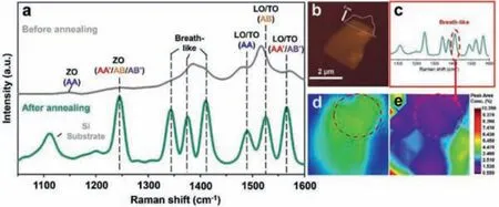
Fig.3.(a) Practical measurement of Raman spectra of stacking C3N.(b) AFM image of the C3N sample for Raman collection.Raman mapping of C3N:(c) Raman spectra of C3N (1050-1600 cm-1), using the breath-like vibration peak located at 1410.0 cm-1 as measuring peak.(d) Total intensity mapping in range of 1050-1600 cm-1.(e) Intensity concentration mapping of specific peak at 1410.0 cm-1.
Interestingly, the inevitable surface defects of C3N can be characterized by Raman spectroscopy.The Raman peaks at 1342.8,1375.6 and 1410.0 cm-1(Table 1) can be due to the breath-like vibration modes, indicating C3N products had a certain number of defective sites.Further confirmation of the surface state of assynthesized C3N was carried out by Raman mapping process (scanning range of 1050-1600 cm-1, sample thickness and lateral size of 1.9-3.7 nm and ~2 μm, respectively, Figs.3b-e), which proved that the oxidation mainly occurred on the surface of C3N.The Raman peak at 1410.0 cm-1(originated from defects) was used as the internal standard peak.Figs.3d and e show the Raman signal intensity of entire sheet and the relative ratio of defect peak area, respectively.For the part inside the red circle (Fig.3d), the Raman signal intensity of entire sheet is relatively strong, which indicates that the thickness of the C3N sheet in this area is thicker.For the same part inside the circle (Fig.3e), the relative ratio of defect peak area was at a lower level.It is shown that the higher the thickness of a single C3N sheet, the lower the defect peak area ratio.The results illustrate defects were mostly on the surface rather than inside of C3N.As reported before, the oxidation occurs on the defect sites of 2D carbon-nitrides [49].It can be suggested that although the C3N was part oxidized with O2in atmosphere or other oxygen-contained solvent molecules, the oxidation process mainly occurred on the surface of products, accompanied by N removal and formation of defective sites.It is consistent with the element analysis as mentioned above (Fig.S2 and Table S3).In addition, a typical HADDF-STEM image of a defective site was shown in Fig.S8(Supporting information), which furtherly proved that defects were simultaneously produced during polymerization process.
In summary, systematic Raman characterization of stacking C3N was firstly investigated detailly with both theoretical calculation and experimental results.The theoretical calculation was carried out to explore the phonon spectrum features for different stacking types of C3N.By use of UV-induced graft polymerization method,high-quality products were obtained.Then practical Raman characterization was investigated and is well agree with the theoretical calculation results.Moreover, we evidenced some structure defects occurred during synthesis process by Raman spectra with other element analysis characterizations.This work gives a comprehensive research on the Raman spectra with different stacking types and reveals abundant structural information of C3N, which broadens the cognition of C3N study.
Declaration of competing interest
The authors declare that they have no known competing financial interests or personal relationships that could have appeared to influence the work reported in this paper.
Acknowledgments
This work was supported by The National Natural Science Foundation of China (Nos.11804353 and 11774368) and Shanghai Science and Technology Committee (No.18511110600).There are no conflicts of interest.
Supplementary materials
Supplementary material associated with this article can be found, in the online version, at doi:10.1016/j.cclet.2021.09.098.
 Chinese Chemical Letters2022年5期
- Chinese Chemical Letters的其它文章
- Recent advances in enhancing reactive oxygen species based chemodynamic therapy
- An integrative review on the applications of 3D printing in the field of in vitro diagnostics
- Recent developments of droplets-based microfluidics for bacterial analysis
- Dynamics and biological relevance of epigenetic N6-methyladenine DNA modification in eukaryotic cells
- Recent progress in advanced core-shell metal-based catalysts for electrochemical carbon dioxide reduction
- Recent advances in carbon-based materials for electrochemical CO2 reduction reaction