
Predicted a honeycomb metallic BiC and a direct semiconducting Bi2C monolayer as excellent CO2 adsorbents
2022-06-20 08:00MnghuiXiChozhngHouyongYngXiFuLingFuXioliChngJiyunGuo
Chinese Chemical Letters 2022年5期
Mnghui Xi, Chozhng H,*, Houyong Yng, Xi Fu, Ling Fu, Xioli Chng,Jiyun Guo
a Institute of Environmental and Energy Catalysis, Shaanxi Key Laboratory of Optoelectronic Functional Materials and Devices, School of Materials Science and Chemical Engineering, Xi’an Technological University, Xi’an 710021, China
b College of Science, Hunan Universtiy of Science and Engineering, Yongzhou 425199, China
c College of Resources and Environmental Engineering, Tianshui Normal University, Tianshui 741001, China
d Department of Physics, Jishou University, Jishou 416000, China
e School of Science, Jiangsu University of Science and Technology, Zhenjiang 212003, China
Keywords:First-principles calculation Global optimization method Monolayer Bismuth carbide compounds CO2 adsorbents Semiconducting
ABSTRACT We predicted two stable two-dimensional materials of carbon and bismuth elements, namely BiC and Bi2C monolayers.The stabilities of two monolayers were examined by cohesive energy, Born criteria, firstprinciple MD simulations and phonon spectra, respectively.By including the spin-orbit coupling effects,the BiC monolayer is a metal and the Bi2C monolayer possesses a narrow direct (indirect) band gap of 0.403 (0.126) eV under the HSE06 (GGA-PBE) functional.For the adsorption of CO2 molecules, the BiC and Bi2C monolayers have three stable adsorption sites C2, T3 and T4 with the adsorption energies as -0.57,-0.51 and -0.81 eV, and the activation ability on the adsorption as T4 >T3 >C2.These consequences make the BiC and Bi2C monolayers to be promising adsorbents to capture CO2 gas, the Bi2C monolayer to be well photovoltaics and optoelectronics material, and the BiC monolayer to be ideal battery and electronics materials, respectively.
Since the discovery of graphene, two-dimensional (2D) layered materials have exhibited excellent electrical, optical and mechanical properties due to their unique electrical structure and quantum confinement effect, and they are widely applied in optoelectronic semiconductor devices, flexible electronic devices, energy storage,and photoelectrocatalysis [1–5].In particular, single-layer 2D materials with atomic thickness, namely monolayers, are attractive for applications in next-generation nanoelectronic devices which may causes low energy consumption [2,3,6-13].Therefore, searching novel, efficient and feasible monolayers manifests important theoretical and practical values.
Bismuth based 2D materials have gradually become a hot research due to a larger number of advantages, such as, very kinds of species, abilities to adsorb visible light for most of materials, narrow band gap energy, low cost and non-toxicity [12–20].Some elemental monolayers of bismuth, such asβ-phase bismuthene with buckled hexagonal honeycomb structure and direct band gap of 0.32 eV andα-phase bismuthene with puckered black-phosphorus style structure, have also theoretically found and experimentally synthesized [15–17].For the binary compounds of group-VA including the bismuth element, BiN [21], BiP [22], BiAs [23], BiSi[24] semiconducting monolayers are all found or experimentally synthesized.On the other hand, for the binary compounds between bismuth and group-IVA family elements, two hexagonal SiBi monolayers with direct/indirect band gap of 0.674/0.4 eV [25,26], a tetragonal SiBi monolayer with indirect band gap of 0.554 eV [27],a metallicα-phase CBi monolayer [28,29] and a Bi2C3monolayer with 12-atoms honeycomb lattices and direct bandgap of 1.23 eV[30] also have been predicted and studied respectively.
It is useful for developing new monolayers as CO2capture or storage materials in the practical applications.Recently, Kumaret al.studied the adsorption of NH3, NO and NO2gas molecules on the surface of a Bi2C3monolayer which can be used as a promising and sensitive sensor for above gasses [31].On that account, by performing structure searching between carbon and bismuth elements using
Crystal structure analysis by particle swarm optimization (CALYPSO) package [32,33], we acquired two new stable monolayers,namely BiC and Bi2C monolayers, and discussed the applications of these monolayers in optoelectronics devices and electrocatalysis on CO2gas capture.
We used the ViennaAb-initiosimulation package (VASP) package and NANODCAL software with the generalized-gradient approximation (GGA)-Perdew-Burke-Ernzerh (PBE) functional to calculate the electronic, mechanical, optical properties, and to perform structure optimization in the predicting course using the CALYPSO package [34].We set the energy cutoff as 600 eV and Monkhorst-Pack scheme as sample Brillouin zone with 0.02 Å-1spacing.The convergent energy per atom was set up to 1.0 × 10⁻⁶eV, and force of atom as no more than 0.001 eV/Å.On account of the large atomic number of bismuth element, spin-orbit coupling (SOC) should be considered when calculating the electronic properties of monolayers, and the HSE06 functional was also adopted to get more exact band gap [18,28,35].Additionally, using the VASP package we implemented the first-principle molecular dynamics (MD) simulations in the NVT with a supercell of 3 × 3 × 1 or 3 × 4 × 1 at different temperatures from 100 K to 1400 K and at the 300 K equilibrium state, respectively.Finally, we employed the PHONOPY package to acquire the phonon spectrum with a supercell size as 4 × 4 × 1 [36].
Prediction were executed using the CALYPSO 6.0 package based on the method of global particle swarm optimization [32,33].In theinput.datfile, we opened the option of predicting 2D materials as2D= T and set the parametersArea= 22,MultiLayer= 1,DeltaZ= 0.3 andVacuumGap= 14 Å to searh BimCnmonolayers.For a composition case, the numbers of generation and population size were 40 and 40 to acquire 1600 structures.The essential parameters in threeINCAR_i(i= 1, 2, 3) files were set asNSW= 60,150, 300,EDIFF= 1e-2, 1e-3, 1e-5andPSTRESS= 0.001, respectively.
In the course of calculating CO2capture, Dmol3program package [37] was used in the whole structure optimization with the basis set as double numeric with polarization (DNP) [38].The basis-set cutoff was set to 4.8 Å, and the K-point grid for Brillouin zones was 3 × 3 × 1 during geometry optimization.The Tkatchenko-Scheffler (TS) method of DFT-D correction [39] was used, and the vacuum layer was 20 Å [40].All electrons in the system use core treatment in the entire structural optimization process and the charge distribution was determined by Hirshfeld analysis [41].Additionally, a gas adsorption simulation was performed on a 2 × 3 × 1 supercell for the BiC structure, and a 2 × 2 × 1 supercell used for the Bi2C structure.In the course of calculating density of states (DOS), charge density difference and Crystal Orbital Hamiltonian Population (COHP) [42] properties, the K-point was set as 6 × 6 × 1.
Geometry structures of the BiC and Bi2C monolayers are shown in Fig.1, and correspondingly their lattice parameters, bond lengths and cohesive energies are also presented in Table S1 (Supporting information).The space group of two monolayers areP1,and unit cells of the BiC and Bi2C monolayers are taken as Bi2C2and Bi4C2.From Fig.1a, the BiC monolayer has honeycomb hexagonal and buckled structures, and its structure in which C and Bi atoms are sp2hybridization, is extremely similar to that ofβ-phase bismuthene [12,18].From Fig.1b, the Bi2C monolayer, which looks like the structure of a buckledα-Bi monolayer [43], is composed of 5-membered rings including C-Bi single and Bi-Bi double bonds.In the structure, each C and Bi atoms form four bonds and three bonds respectively, all exhibiting sp3hybridization.
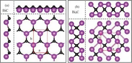
Fig.1.Top and side views of (a) BiC and (b) Bi2C monolayer.Black and purple balls represent carbon and bismuth atoms, and their unit cells are shown in the top views.
In Table S1, lengths of C-Bi bonds are 2.316 Å for the BiC monolayer, 2.317 Å and 2.319 Å for the Bi2C monolayer respectively,and there do not show relatively large differences to the lengths of Bi2C3monolayer (2.31 Å) and CBi monolayer (2.38 Å) [27,28].Lengths of Bi-Bi bonds are 3.153 Å for the Bi2C monolayer, which are the same as that of 3.13 Å in the bismuthene or much smaller than that of 4.92 Å in the SiBi monolayer [18,44].The bond lengths in two Bi-C monolayers are normal indicating they should be stable 2D materials.
Furthermore, we calculated their cohesive energyEcohfrom the following formula:
whereEBimCn,EBiandECare the energy of monolayer, one free Bi and one free C atom, respectively.As shown in Table S1,Ecohfor the BiC and Bi2C monolayers are 4.304 and 4.29 eV/atom respectively, which are slightly samller than that of 4.66 eV/atom for the Bi2C3monolayer [30], larger than that of 4.13 eV/atom for the CBi monolayer [28], 3.227 eV/atom for the SiBi monolayer [24],2.896 eV/atom for the GeBi monolayer [27] and 2.697 eV/atom for the SnBi monolayer [27] respectively, further implying the stability of two Bi–C monolayers.
In order to show formation of bonds and charge transfer of two Bi–C monolayers, we calculated electron localization functions(ELFs) shown in Fig.S1 (Supporting information), and performed bader analysis presented in Table S2 (Supporting information) [45].From Figs.S1a and b, two Bi–C monolayers exhibit electron collections between C and Bi, C and C, Bi and Bi atoms, indicating the formation of C–Bi, C–C, Bi–Bi bonds.In addition from the top and side views, there exist a mass of electrons around the Bi atoms,which leads to their metallic or semiconducting features.From Table S2, one can find that in the BiC monolayer about -0.802 charges and in the Bi2C monolayer -0.516 and -0.503 charges transfer from the Bi to the C atoms respectively, manifesting the formation of C-Bi bonds in two Bi-C monolayers.
Firstly, to study dynamic stability of two Bi–C monolayers, we calculated their phonon dispersion displayed in Figs.S2a and b(Supporting information).One can see that for the BiC and Bi2C monolayers no negative phonon frequencies exist which manifests two Bi–C monolayers are kinetically steady.Moreover, the slopes of acoustic branches for the BiC monolayer are identical along different orientations, such as G-M, G-K, showing it is isotropic related to the in-plane stiffness, and for the Bi2C monolayer its different slopes of acoustic branches indicate anisotropic property accordingly.
Secondly, we examined mechanical stability of two Bi–C monolayers by calculating their elastic constants (Cij).A mechanically stable 2D material should be conform to the Born criteria:C11>0,C11C22>(C12)2,C66>0 [46].By fitting the energy curves relevant to in-plane stresses,Cijwere inferred asC11= 54.75 N/m,C22= 54.52 N/m,C12=C21= 16.38 N/m,C66= 4.814 N/m for the BiC monolayer, andC11= 13.21 N/m,C22= 33.56 N/m,C12=C21= 5.06 N/m,C66= 0.95 N/m for the Bi2C monolayer,respectively.These elastic constants are in accord with the Born criteria indicating their mechanical stability.Based on above elastic constants, in-plane Young’s modulesYxandYycan be deduced as 49.83 and 49.62 N/m for the BiC monolayer, 12.44 and 31.62 N/m for the Bi2C monolayer, respectively.These values are smaller than those of MoS2monolayer (<128 N/m), silicene (61 N/m) while the same as those of BiN monolayer [19,47], indicating two monolayers are relatively soft.
Finally, we performed first-principles MD simulations with a relatively large supercell 4 × 3 × 1 for the BiC monolayer,3 × 3 × 1 for the Bi2C monolayer, respectively.After executing 10 ps simulations from 100 K to 1400 K, the structures of two monolayers maintain very well.We also executed 50 ps equilibrium simulations for two monolayers at the temperature 300 K which are shown in Fig.S3 (Supporting information).From Figs.S3a and b, the energy is oscillating near the equilibrium state and the structures of two monolayers are preserved well, displaying the thermal stability of two Bi-C monolayers which are anticipated to be experimentally practicable.
We calculated band structures and DOS of two Bi-C monolayers using the GGA-PBE and HSE06 functional, and the SOC effect was also considered to obtain more accurate band gap.Figs.S4a and b (Supporting information) show their band structures with/without SOC using the GGA-PBE functional and correspondingly high points are presented.When the SOC effect included, energy bands of two Bi-C monolayers all appear Rashba-type splits from the top of valence band.Additionally, this splitting will affect the positions of conduction band maximum (CBM) and valence band maximum (VBM) of two Bi-C monolayers and certainly deduce the changes of band gap [18,48].Rashba coupling is one type of intrinsic SOC effects for possible control of spin states without a magnetic field, and can lead to spin degeneracy owing to structural inversion asymmetry [18].
Furthermore, in order to obtain precise band gap close to experimental possibilities, we also calculated band structures and DOS of two Bi-C monolayers including the SOC effect, which are displayed in Fig.2.The BiC monolayer is metallic under the GGA-PBE(HSE06) functional.Its DOS strengths smaller than 0.5 eV mainly come from C atoms, and DOS strengths larger than 0.5 eV mainly come from Bi atoms.Moreover its DOS strengths for the p-orbital of all atoms are bigger than those of the s- and d-orbitals.The Bi2C monolayer is an indirect (direct) semiconductor with the band gap as 0.126 (0.403) eV under the GGA-PBE (HSE06) functional.Moreover, the DOS of Bi2C monolayer mainly comes from p-orbital of Bi atoms, and DOS strengths of Bi atoms are larger than that of C atoms.These results on the DOS verify that the carriers in two Bi-C monolayers mainly originate from Bi atoms or Bi p orbital once again.Liking the bismuthenes [18,49], the Bi2C monolayer is a narrow direct semiconductor, which makes it as an ideal 2D material in the applications of optoelectronics and photocatalysis.On the other hand, in view of metallic speciality and honeycomb hexagonal structures liking graphene of the BiC monolayer, it can be as a potentially ideal battery or electrocatalysis material.
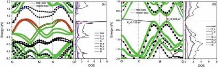
Fig.2.Band structures and DOS of (a) BiC and (b) Bi2C monolayer with the GGA-PBE/HSE06 functional and the SOC effect.Green and red/black and blue rounds represent the weight of Bi and C atoms for the GGA-PBE/HSE06 functional, respectively.
Base on band structures, we further calculated carrier mobilities of the Bi2C monolayer in consideration of its semiconducting, as shown in Table S3 (Supporting information) under the GGA-PBE functional.From the table, only the effective mass affects their carrier mobilities, then the mobilities were calculated asμx= 194.67,μy= 139.05 cm2V-1s-1for the electrons, andμx= 69.22,μy= 6.38 cm2V-1s-1for the holes respectively.The electron mobility alongxdirection is similar to the values of MoS2(200 cm2V-1s-1) and Bi2C3monolayer (186 cm2V-1s-1) [28,50],displaying the Bi2C monolayer is still a good semiconducting 2D material potentially applied in nanoelectronics.
It is great need to develop an efficient CO2removal system,and two-dimensional materials are considered as efficient CO2adsorbents [51,52].To describe the interaction between CO2and BiC/Bi2C monolayer, we defined the adsorption energyEadas:

whereEall,EsubandEgasrepresent total energy of adsorbed monolayer, pritine BiC/Bi2C monolayer and the CO2molecule, respectively.The charge density differenceΔρfor the complexes was calculated by following equation:

whereρall,ρsubandρgasare charge density of adsorption system,BiC/Bi2C monolayer and the CO2molecule, respectively.
The adsorption of a single CO2gas molecule on the BiC monolayer was computed.In order to explore the most stable adsorption structure, several traditional adsorption sites were selected on the six-membered ring of BiC monolayer, namely top position of Bi atom (T1 site), hollow position (H1 site) and bridge position (Br site) of Bi–C bond, top position (C1 site) and back position (C2 site)of C atom, as shown in Figs.3a and d.After calculations, the corresponding adsorption energies of five adsorption sites (T1, H1, Br, C1,C2) are -0.41, -0.21, -0.44, -0.25, -0.57 eV, respectively.Smaller the negativeEadis, accordingly stronger the interaction and the exothermic reaction, which proves that the adsorption is reasonable and easy to occur.
According to the above data, it is easy to see that the C2 site is the most stable position for the adsorbed CO2gas molecule on the BiC monolayer, and corresponding most favorable adsorption structure was shown in Figs.3b and e.From the figures it can be concluded that compared with free state CO2molecule, after being adsorbed the molecular configuration has been significantly bent,in which the ∠O–C–O bond angle is reduced from 180° to 124.3°and the C–O bond lengths are stretched from 1.177 Å to the maximum of 1.338 Å by 14%.The adsorption distanceDabetween the monolayer and the substrate is 1.150 Å, which shows that the CO2gas has been violently activated on the BiC monolayer, and the BiC monolayer may have potential applications for CO2catalytic reduction.
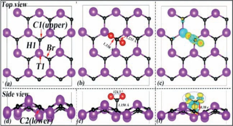
Fig.3.(a, d) Top and side views of tested adsorption sites on the BiC monolayer.(b, e) The structure of BiC monolayer with the CO2 adsorbed on the C2 site.(c, f)Corresponding difference charge density of BiC monolayer, and yellow/cyan area is the part where the charge density increases/decreases with the isosurface value as 0.008 e-/Bohr3.
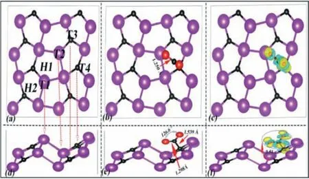
Fig.4.(a, d) Top and side views of tested adsorption sites on the Bi2C monolayer.(b, e) The structure of Bi2C monolayer adsorbed CO2 molecule at the T4 site.(c, f)Corresponding difference charge density of Bi2C monolayer.
When theEadis greater than -0.50 eV, gas molecules can be effectively captured by the adsorbent [53].Because theEadof CO2molecule at the C2 site is -0.57 eV which corresponding to significant changes of the configuration for the CO2molecule, and by the Hirshfeld charge analysis it is easy to figure that the CO2molecule obtains 0.38e-from the substrate during the adsorption process.Compared with the charge of C atom in the free state CO2molecule, the charge of C atom decreased from 0.30e-to 0.11e-,and the charge of O atoms increased from -0.15e-to -0.25e-,which is also consistent with the information reflected by charge density difference in Figs.3c and f.In Figs.3c and f, the electron density at the position of C atom in the CO2molecule decreases,while more electrons concentrate between the gas molecule and the monolayer, which indicates that C–O bond became weaken and a strong interaction between CO2molecules and BiC monolayer.
Using the same adsorption test method, for the Bi2C monolayer we chose the adsorption sites of CO2molecule as H1 and H2 (hollow sites), T1 (top site of raised Bi atoms), T2 (top site of sunken Bi atom), T3 (top site of C atoms in the lower layer), and T4 (top site of C atoms in the upper layer) respectively.Figs.4a and d show six selected adsorption sites, and corresponding adsorption energyEadis 0.62, 0.67, -0.10, 1.22, -0.51, -0.81 eV.From Figs.4b and e the configuration of CO2molecular at the T4 site has significantly changed due to strong adsorption interaction of the Bi2C monolayer, in which the ∠O–C–O bond angle is reduced from 180° to 126.6° and the C–O bond lengths are stretched from 1.177 Å to the maximum of 1.298 Å by 16%.The adsorption distanceDabetween the CO2molecular and the Bi2C monolayer is 1.539 Å, which is larger than that of BiC monolayer.Figs.4c and f show that the CO2molecule gets 0.54e-from the Bi2C monolayer with the charge of C atoms changed from 0.30e-to 0.08e-and the charge of O atoms increased to -0.30e-.Corresponding charge density distribution diagram also indicates that there have distinct electrons flowing from C atoms to O atoms in the CO2molecule.
Similarly in Fig.S5 (Supporting information), the C atom at the T3 site can also effectively captures a CO2gas molecule with theEadas -0.51 eV.From Figs.S5b and e, the bond length and bond angle of CO2molecule also changed obviously under the action of C atom at the T3 site, in which ∠O–C–O bond angle is reduced from 180° to 126.2°, and the C–O bond lengths are stretched from 1.177 Å to the maximum of 1.280 Å by 15%.The results on the Hirshfeld charge analysis show that the CO2molecule obtains 0.49echarge from the Bi2C monolayer after adsorption, and the map on the electron density difference presents that the electron population in the CO2molecule is transferred from the C atom to two O atoms.According to the analysis of above consequences on the degree of activation to C–O bonds (16%>15%>10%), the rank of activation ability for three sites on the adsorption of CO2molecule is T4 (Bi2C)>T3 (Bi2C)>C2 (BiC).
It is well known that the activation of C–O bonds in the CO2catalysis process is a prerequisite for the reduction process [54].In order to figure out the activation of C–O bonds in the CO2molecule, we use molecular orbital theory [55] to study why the CO2molecule can be activated on the BiC/Bi2C monolayer.Fig.S5d shows the molecular orbital of free CO2molecule, and the smaller the difference in the energy level of atomic orbital, the stronger the performance ability of composed molecular orbital.Combining the DOS and COHP in Fig.S6a (Supporting information), it can be known that the bonding orbitals 1σ2σ1π2πof C–O bonds in free CO2molecule are mixed contributed by C pz, O pz, O py, C py, C px,O pxatomic orbitals, and the non-bonded states are mainly composed of O px, O pyand C pzwhose energy levels are around Fermi level.The anti-bond state is mainly contributed by the combination of C px, C py, C pzand O py, respectively.From Fig.S6b (Supporting information) it can be seen that due to the activation at the T3 site of Bi2C monolayer, the bonded and non-bonded states of CO2molecule have undergone significant changes.Moreover, the corresponding bonded state has shifted to a deeper energy level from -4.2 eV to -6.3 eV, and the non-bonded state has shifted from -4.5 eV to 0 eV which corresponding to a wider range.The bonding state of C–O bonds at this time is mainly composed of the contributions of O px, O pzand C pyatomic orbitals.The contribution of O pyatomic orbital to the non-bonded state and the area of anti-bonding state increase, indicating that due to more antibonding orbitals the C–O bonds are weakened after the linearly mixing of atomic orbitals again.
Similarly, by comparing Fig.S6c (Supporting information) at the T4 site of Bi2C monolayer with Fig.S6b, one can conclude that the bonded states are mostly composed of O p and C p atomic orbitals which localized around -6.2 eV, and the range of non-bonded states from -4.1 eV to 0 eV mainly composed of O p orbitals which is not as wide as that of the T3 site.Compared to the area of antibonding state shown in Fig.S6a, the area of anti-bonding state in Fig.S6c is increased, indicating that the C–O bonds are also weakened atomic orbitals.As for the C2 site of BiC monolayer to activate the CO2molecule in Fig.S6d (Supporting information), we find that the non-bonded orbitals are mainly composed of C px, C pyand C pzatomic orbitals, and the range of bonded states (mainly concentrated at -5.5 to -6.1 eV) are mainly composed of C px, C pyand C pzcontribution composition.
The Intergral Crystal Orbital Hamiltonian Population (ICOHP) of C–O bonds at the T3, T4 and C2 sites are -12.52, -12.10 and -11.14 respectively, which are reduced by 31.9%, 34.2% and 39.4% compared with free CO2molecule case, and further proved the activation of C–O bonds.In summary, the reason why BiC/Bi2C monolayer is more capable of activating the C–O bonds in the CO2molecular is that the C atom (bonded with Bi atom) regulating the electronic structure of CO2molecular, which resulting the changes of CO2molecular orbital distribution.The BiC and Bi2C monolayers can be used as promising adsorbents to capture CO2gas aiming to mitigate the greenhouse effect.
In conclusion, we used the CALYPSO methodology obtaining two bismuth carbide monolayers.By including the SOC effect, the BiC monolayer is a metal and the Bi2C monolayer is a direct semiconductor with the band gap as 0.403 eV.For the adsorption of CO2molecules on two monolayers, the BiC monolayer has one stable site C2, and the Bi2C monolayer has two stable sites T3 and T4.Based on the molecular orbital theory and ICOHP analysis, the rank of activation ability for three sites on the adsorption of CO2molecules is T4>T3>C2.Therefore, one can concluded that the BiC and Bi2C monolayers are promising adsorbents to capture CO2gas being expected to mitigate the greenhouse effect.The Bi2C monolayer also has a wide scope of applications in the optoelectronics and photocatalysis for its narrow direct band gap and good carrier mobility.As to the Bi2C monolayer, it is metallic and may be applied in the energy storage battery.
Declaration of competing interest
The authors declare that they have no known competing financial interests or personal relationships that could have appeared to influence the work reported in this paper.
Acknowledgments
We thank hongzhiwei cloud platform to provide computer time.This study was funded by the Natural Science Foundation of China(Nos.21603109, 11304128), the Henan Joint Fund of the National Natural Science Foundation of China (No.U1404216), the Science and Technology Program of Henan Department of Science and Technology, China (No.182102310609), and the Construct Program of Applied Characteristic Discipline in Hunan University of Science and Engineering (Mathematics, Education and Electronic Science and Technology).
Supplementary materials
Supplementary material associated with this article can be found, in the online version, at doi:10.1016/j.cclet.2021.12.041.
 Chinese Chemical Letters2022年5期
- Chinese Chemical Letters的其它文章
- Recent advances in enhancing reactive oxygen species based chemodynamic therapy
- An integrative review on the applications of 3D printing in the field of in vitro diagnostics
- Recent developments of droplets-based microfluidics for bacterial analysis
- Dynamics and biological relevance of epigenetic N6-methyladenine DNA modification in eukaryotic cells
- Recent progress in advanced core-shell metal-based catalysts for electrochemical carbon dioxide reduction
- Recent advances in carbon-based materials for electrochemical CO2 reduction reaction