
Encapsulation strategies on 2D materials for field effect transistors and photodetectors
2022-06-20 07:59WenjunHungYueZhngMengtingSongBugoWngHuyiHouXiozongHuXingbiChenTinyouZhi
Chinese Chemical Letters 2022年5期
Wenjun Hung, Yue Zhng, Mengting Song, Bugo Wng, Huyi Hou,Xiozong Hu, Xingbi Chen,*, Tinyou Zhi
a Hubei Key Laboratory of Optical Information and Pattern Recognition, Wuhan Institute of Technology, Wuhan 430205, China
b State Key Laboratory of Materials Processing and Die &Mould Technology, School of Materials Science and Engineering, Huazhong University of Science and Technology, Wuhan 430074, China
c Green Catalysis Center, College of Chemistry, Zhengzhou University, Zhengzhou 450001, China
Keywords:Two-dimensional materials Encapsulation Degradation Stability Field effect transistors Photodetectors
ABSTRACT Two-dimensional (2D) layered materials provide a promising alternative solution for overcoming the scaling limits in conventional Si-based devices.However, practical applications of 2D materials are facing crucial bottlenecks, particularly that arising from the instability under ambient condition.The studies of degradation mechanisms and protecting strategies for overcoming the ambient instability of 2D materials have attracted extensive research attentions, both experimentally and theoretically.This review attempts to provide an overview on the recent progress of the encapsulation strategies for 2D materials.The encapsulation strategies of mechanical transfer, polymer capping, atomic layer deposition, in-situ oxidation,and surface functionalization are systematically discussed for improving the ambient stability of 2D materials.In addition, the current advances in air-stable and high-performance 2D materials-based field effect transistors (FETs) and photodetectors assisted by the encapsulation strategies are outlined.Furthermore,the future directions of encapsulation techniques of 2D materials for FETs and photodetectors applications are suggested.
1.Introduction
With the rapid development of integration and miniaturization of modern microelectronic industry, conventional Si-based complementary metal oxide semiconductor (COMS) devices are facing a bottleneck of scaling limit caused by short-channel effect.To address this problem, researchers are striving to explore innovation materials to replace silicon channel materials [1,2].Ultrathin twodimensional (2D) layered materials provide the great opportunities for overcoming the bottleneck of silicon because their thickness can be scaled down to monolayer limit [3,4].In the past decade, 2D materials have become promising candidates for highperformance field effect transistors (FETs) and optoelectronic devices due to their exceptional properties [5–8]:(1) ultrathin thickness and atomic flatness without dangling bonds, enabling them robust electrical performance free from carrier scattering, excellent gate controllability and strong light-matter interaction for highperformance devices applications; (2) adjustable bandgaps in a wide range with thickness change, contributing them fascinating optoelectronic features; (3) arbitrary ‘lego’stacks heterostructures without considering lattice mismatch, facilitating purposefully designed or multifunctional electronic and photonic devices; (4) excellent mechanical flexibility, making them more compatible with the current micromanufacturing techniques.
Since the discovery of graphene in 2004 [9], versatile graphenelike layered 2D materials with strong in-plane bonds and stacked by weak van der Waals interlayer forces have been explored in the field of electronics and optoelectronics.Graphene has proven to be a promising material for high-speed electronics and optoelectronics due to its ultrahigh carrier mobility, wide-band absorption and fast photoresponse [10].However, graphene-based FETs have poor on/off current ratio and cannot be effectively switched off owing to its zero bandgap, which restricts its real circuit applications [11].In contrast, several 2D layered materials possess sizable bandgaps with extraordinary electronic and optical properties, showing the promising interests in novel FET and optoelectronic devices [12].Black phosphorus (BP) has widely thicknessdependent electronic bandgaps from 0.3 eV for bulk to 2.0 eV for monolayer and high room temperature carrier mobility up to 1000 cm2V-1s-1, making it great potential in various application,such as ultrafast photodetectors and FETs [3,13].Another representative 2D metal chalcogenides including transition metal dichalcogenides (TMDs) (with chemical formula of MX2, where M consisted of transition metale.g., Mo, W, Re, Nb or Hf coordinated with X, chalcogene.g., S, Se or Te), group III metal chalcogenides (e.g.,InSe, In2Se3, GaSe, GaTe) [7,14], group IV metal chalcogenides (e.g.,SnS2, SnS, GeSe) [15] have been one of the most extensively studied classes of 2D materials due to their wide range of bandgaps,unusual physical properties and excellent electronic characteristic, leading to the potential applications in FETs, photodetectors or photovoltaic cells,etc.For example, FETs based on MoS2can achieve room temperature charge carrier mobilities in excess of~102cm2V-1s-1with large on/off current ratios up to ~108[16].Carrier mobilities of InSe can reach up 103cm2V-1s-1at room temperature due to weak electron-phonon scattering and optical activity in absorption and emission [7].
In spite of those promising advantages, due to their large surface-to-volume ratio, most 2D materials are more sensitive to the environment when exposure to the ambient air compared with conventional bulk semiconductors [17].Generally, the degradation factors are coming from the intrinsic nature of instability of 2D materials, such as chemical bonds and atomic-level defects [18],associated with external factors such as adsorption of oxygen and water and light illumination [19–21].Among these materials, BP is the most representative materials, oxidation occurs spontaneously when they exposed to the air, which exhibit a discernible surface morphological change even within a few minutes [22].It has been demonstrated that BP is very reactive to oxygen and water under ambient conditions, resulting in compositional and physical changes and consequently considerable degradation in the electronic and optical properties [21].Accordingly, the performance of devices based on these 2D materials would be severely degraded.With considering their bonding states at the surface of 2D materials, graphene and hexagonal boron nitride (h-BN) hold the most stability and remain intact within a few weeks under ambient environment, followed by TMDs, which can preserve almost intact in a few hours [17,23].It has been reported that TMDs are unstable under air over 6 months, and it is believed that the observed degradation begins at the TMD grain boundaries [18,24].Combining theoretical and experimental studies, a series of defectfree 2D materials with perfect crystal are relatively stable, while chalcogen vacancies on the surface can interact with ambient reactants chemically, resulting in a degradation of those 2D materials[17,18], such as MoS2[18], InSe [25], GaSe [26].Such spontaneous oxidation can go deep into the inner layers because of the loose structure of the resulting oxides and leads to a considerable current hysteresis and an uncontrollable p-doping in transistor operations [27,28].For example, InSe exhibit high sensitivity to moisture and oxidation occurs spontaneously as exposed to the air, resulting in the oxidation of In2+into the relatively stable In3+due to the lower free energy of the chemical compound composed of In3+[29].Accordingly, a surface oxidation layer can easily form on the surface of InSe as exposed to the ambient air.Such uncontrolled oxidation at ambient air may usually result in a considerable current hysteresis and cause serious degradation [30].
In order to promote the application of 2D materials in electronic and optoelectronic devices, it is urgent to develop innovation methods for protecting 2D materials from ambient degradation.Lots of efforts have been made to improve the stability of 2D materials.Herein, we review the recent progress of the considered 2D materials including TMDs, BP, groups III-VI and IV-VI metal chalcogenides, and mainly focus on the encapsulation methods for their electronic and optoelectronic applications.First, we briefly summarize the encapsulation strategies of 2D materials including mechanical transfer, polymer capping, atomic layer deposition,in-situoxidation and surface functionalization.Then, we present recent development of these methods employed to achieve stable and high-performance 2D-based device applications in electronics and optoelectronics.Finally, the summary and outlook are presented towards the future applications of encapsulation on 2D materials.
2.Encapsulation strategies
Ambient degradation limits the performance of 2D materials based devices, thus, stabilizing 2D materials to achieve stable and high-performance devices is crucial to their applications.In this section, we will discuss the current encapsulation strategies including mechanical transfer, polymer capping, atomic layer deposition,in-situoxidation and surface functionalization (Scheme 1).Generally, two protecting ways are involved in those encapsulation strategies.One is adopting a protecting layer to effectively isolate 2D materials from environmental active species such as oxygen and water.The other is covalent or non-covalent functionalized by organic and inorganic substance to make their surface environmental inert.Of course, in practical applications, they are often combined with each other to further improve the stability of 2D materials.
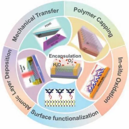
Scheme 1.Schematic illustration of the five encapsulation strategies for improving the stability of 2D materials.
2.1.Mechanical t ransfer
Mechanical transfer is a feasible method in 2D materials and their heterostuructures production and processing process, where the bottom 2D material is transferred another material on top of itviaa supporting medium.Polymethyl methacrylate (PMMA) and polydimethylsiloxane (PDMS) are the most adopted medium layers as they can be easily removed afterwards [31].Owing to their exceptional thermal and chemical stabilities, h-BN, graphene and MoS2are usually used as the protective layer involved in the drytransfer or wet-transfer method against oxidation for the atomically thin 2D materials [23,32–34].Without considering lattice compatibility, various 2D heterostructures and sandwiched encapsulation of 2D materials are formed to enhance their stability over a long time under ambient exposure, such as h-BN-MoS(Se, Te)2[32,35–37], h-BN-BP [33,38–40], h-BN-InSe [30,41,42], graphene-BP[43,44], MoS2-BP [34] and BN-WSe2[45].Doganovet al.[39] reported that the degradation of BP could be suppressed by graphene and h-BN by a dry-transfer method with PMMA support layer in the glovebox.From the AFM images (Figs.1a-c), the obtained sampled encapsulated with graphene (within 24 h) and h-BN (with 5 days) didnot show any noticeable surface change as compared with the unprotected surface of the ultrathin BP crystal.Besides, the stability of the device based on h-BN sandwiched BP nanosheet exhibited no quality degradation after exposure in air for one week.Similarly, Sonet al.[34] demonstrated that MoS2-encapsulated BP can maintain stability in air for 3 weeks even after annealing at high temperature, which can be verified by Raman peaks (Figs.1df).Moreover, the formed heterojunction can add a new functionality of electrical transport to BP due to the p-n junction between BP and MoS2, which can be used to enhance the photoresponse due to dissociation of photo-generated electron–hole pairs at heterointerface.Mercadoet al.[46] demonstrated that the degradation process in GaTe flakes can be slowed down dramaticallyviadouble encapsulation with both top and bottom graphene.As shown in Figs.1f and g, the photoresponse of GaTe flakes encapsulated in this way can be reduced by 17.6% ± 0.4% after 2 weeks,whereas unencapsulated flakes displayed no response after this time.
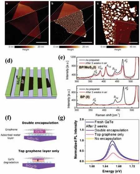
Fig.1.(a,b) Atomic force microscopy (AFM) images of a 5-nm-thick BP crystal partly covered with graphene, which were acquired 10 min and 24 h after exposure to ambient conditions, respectively.The white dashed lines outline the passivating graphene crystal.(c) AFM scan of a 10-nm-thick BP crystal partly covered with h-BM after 5 days in ambient conditions.Scale bar, 4 mm (for all images).Copied with permission [39].Copyright 2015, Nature Publishing Group.(d) Schematic illustration of the BP-MoS2 FET devices.(e) Raman spectra taken at exposed (bottom)and MoS2-passivated BP (top) upon preparation and in 3 weeks in air.Copied with permission [34].Copyright 2017, IOP publishing.(f) Schematic illustration of double encapsulation (top) and top graphene layer (bottom) for GaTe flakes.(g) PL spectra of freshly exfoliated GaTe, without, double and top encapsulation after 14 days of ambient exposure.Copied with permission [46].Copyright 2019, American Chemical Society.
To sum up, encapsulation with 2D materials by mechanical transfer method could be used to enhance the desirable qualities of other 2D materials for their device applications.In particular,benefit from its atomic smooth surface and dielectric characteristics, h-BN can also be as gate dielectric to achieve remarkable electrical properties for various 2D materials by effectively suppressing carrier scattering from the surface absorbents of O2and H2O[37–39,47], which will be discussed in device applications.Nevertheless, encapsulation with mechanical transferred 2D materials requires complex manipulations and is not practical for scaling up and integration.An efficient and scalable method is urgently needed for the encapsulation of 2D materials.
2.2.Polymer capping
Polymer capping provides an efficient and scalable strategy for protecting 2D materials from environmental degradation.To encapsulate polymer on 2D materials, the common methods includes spin-coating [48–51], dip-coating [52], drop-casting [53], vapor deposition [22,54],etc.Owing to its high-k dielectric properties and easily scalable process, PMMA is one of the most commonly used encapsulation capping layer on various 2D materials with longterm stability upon exposure to ambient air [49,55,56].For example, Jiaet al.[55] encapsulated BP-based device with PMMA immediately after the plasma etching process for controlling the thickness film (Fig.2a), which showed a high mobility up to 1150 cm2V-1s-1and high-stability over several weeks.Similar work has been reported in Liet al.’s work [57], they found both the hole and electron mobilities of the PMMA encapsulated BP-FET are almost unchanged up to 50 h (Fig.2b).After spincoating PMMA on MoS2device, the PMMA-sandwiched MoS2transistor also exhibited a stable electrical properties during the roomtemperature storage in air up to 45 days [49].In addition to isolating the surface of 2D materials from the atmospheric environments, polymer with high-k dielectric has also been seen to modify the channel properties.For example, cross-linked PMMA can modify the potential in a BP layer so that conduction in the absence of an external electric field is dominated by electrons, rather than holes [58].Besides PMMA, there are many other polymers such as polyvinyl pyrrolidone (PVP) [59], polyvinyl alcohol (PVA)[60], polyethyleneimine (PEI) [61], fluoropolymer CYTOP [50,62,63],SU8 [48,53], and parylene C [22] with similar function used to protect 2D materials from degradation to improve device performances.Kunget al.[53] demonstrated a highly stable multilayer MoS2FETs with long-term air stability for 9 days after SU8 encapsulation and exhibited only minor changes in the transfer characteristic (Figs.2c and d).
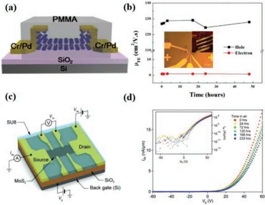
Fig.2.(a) Schematic diagram of PMMA-encapsulated BP FET.Copied with permission [55].Copyright 2015, American Chemical Society.(b) The dependence of electron and hole mobilities on the storage time for the PMMA-encapsulated BP FET.The insets are the optical image and the AFM image of the device.Copied with permission [57].Copyright 2019, IOP publishing.(c) Bottom-gated monolayer MoS2 FET with SU8 coating.(d) The evolution of the transfer characteristic for an SU8-doped MoS2 FET kept in air over 9 days.Copied with permission [53].Copyright 2019, John Wiley & Sons Ltd.
However, encapsulation using polymers is usually accompanied by curing process, unpredictable and troublesome problems will be induced from their low glass transition temperature, which poses a considerable challenge to their incorporation into functional devices.
2.3.Atomic layer deposition
Atomic layer deposition (ALD) is a highly scalable and manufacturable technique to prepare conformal and pinhole-free highk dielectric thin films for gate insulator and diffusion barrier applications in conventional Si-based COMS devices, which involves the reaction of metal precursors (e.g., trimethylaluminum) and an oxidation agent (water or ozone) that react with the surface separately in a self-limiting [64].ALD of high-k dielectrics such as aluminum oxide (Al2O3) [65–67], zirconium oxide (ZrO2) [68] or hafnium dioxide (HfO2) [69–71] is also extended to 2D materials[51,62,67,72].ALD encapsulation AlOxlayer has been extensively explored to protect BP from air degradation [65,66].As shown in Figs.3a and b, it can be observed that AlOxlayers can effectively suppress ambient degradation, allowing encapsulated BP FETs to maintain high on/off ratios of ~103and mobilities of~100 cm2V–1s–1for over 2 weeks in ambient conditions through the dielectric screening on Coulomb scattering and to provide effi-cient moisture and oxygen permeation barriers [65].Moreover, Illarionovet al.reported that BP FETs with conformal 25 nm Al2O3encapsulation exhibited a highly-stable performance up to ~17 months [73].However, ALD cannot be used for the encapsulation of ultrathin BP samples, because the oxygen precursor would simultaneously degrade thin BP during ALD process [22,74].Alternatively, Wellset al.[67] developed a low-temperature ALD encapsulation method for InSe nanosheets, which allowed InSe-based FETs and photodetectors to be operated in air with high stability even after ambient exposure on the time scale of months.In addition, it is well known that ALD growth is not suitable for 2D materials due to their inert basal plane [75,76].Island growth is often observed on the 2D surface because of sparse density of nucleation sites [77,78].In order to enhance nucleation on 2D surfaces, plasma-enhanced ALD (PEALD) has been developed [71,79].Recently, Priceet al.[71] used PEALD to deposit HfO2on MoS2,the related schematic illustration is shown in Fig.3c.By using experimental characterization and theoretical calculations, they revealed that a competing relationship between the dielectric thickness scaling, 2D materials thickness scaling, and device electrical properties that stem from the inertness of the surface of 2D materials.Encapsulation using high-k dielectric not only protects the 2D materials against air degradation but has also been seen to reduce Coulomb scattering from the charged traps or impurities [69,80].
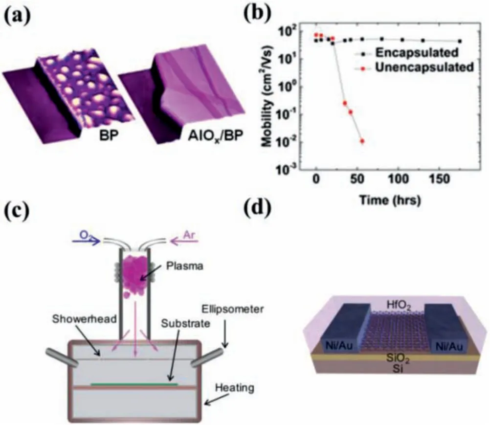
Fig.3.(a) Encapsulation of exfoliated BP by atomic layer deposited AlOx over layers.(b) Hole mobility for encapsulated and unencapsulated Ti/Au BP FETs versus ambient exposure time.Copied with permission [65].Copyright 2014, American Chemical Society.(c) Schematics illustrating the ALD/PEALD reaction chamber.(d)PEALD of HfO2 encapsulation layer on MoS2 device.Copied with permission [71].Copyright 2019, American Chemical Society.
Although ALD encapsulation strategy can provide both longterm stability and excellent device performance for 2D materials,the ALD-processed oxides show non-uniform growth and can damage ultrathin 2D materials, leading to severe n-type doping [81].
2.4.In-situ oxidation
It is known that the growth of high-quality oxide film on a semiconductor with a controllable manner is a key factorfor the advanced Si-based electronic and optoelectronic devices [82].Insituoxidation is a powerful encapsulation method and has been recently developed to protect 2D materials-based devices from ambient degradation, which can be achieved by ambient exposure[28,83–85], UV-ozone (UVO) exposure [86–89], O2plasma treatment [81,90–94], or thermal treatment in oxygen rich environments [28,83,85,95].Native oxide formed on the surface can stabilize the underlying 2D materials from further oxidation.Peiet al.[92] used O2plasma layer-by-layer etching BP followed by further passivation with an Al2O3coating to obtain air-stable few- or monolayers of BP (Fig.4a).During the O2plasma treatment process, the top layers of the phosphorene flake were oxidized to be PxOy,which then served as a protective layer for the remaining phosphorene sample underneath.Similarly, the stability of the BP can be improved by thermal treatment of BP in air and the device based on it remained for 1 month under ambient condition without an additional protecting layer, resulting from the preservation of active BP layers below native surface PxOy(Fig.4b) [95].Due to the presence of lone-pair states of Se at the top of the valence band, InSe surface is prone to adsorb gas molecules [28,91].Hoet al.[28] introduced a dry oxidation on as-exfoliated InSe flakes to form a dense oxide layer that can keep the inner InSe layers intact as exposed to the air.It was found that the InSe covered with dry oxide shares the same Raman characteristic peaks with the pristine one, indicating the formation of nonstoichiometric thin oxide InSe1-xOx(Fig.4c).As compared with the cases of air oxidation in air, no amorphous In2Se3was formed until aging in air for more than one week (Fig.4d).After aging in air for a week, no bumps or bubbles are found, indicating that the oxide is chemically stable and does not react with moist water (Fig.4e).Such an encapsulation route not only improves the stability of 2D materials, but also enables a range of 2D materials structural and chemical modifications.For TMDs crystal with certain concentration of defects, oxygen can spontaneously blend into TMDs surface to replace sulfur vacancies forming non-stoichiometric metal oxide (MO3-x) under O3or O2plasma exposure due to their isoelectronic nature [86–88,94,96], leading to p-type doping of TMDs.Several studies also showed that the formed dense metal oxide can enhance their conductivity and photoluminescence intensity, further improve device performance built on them [97,98].
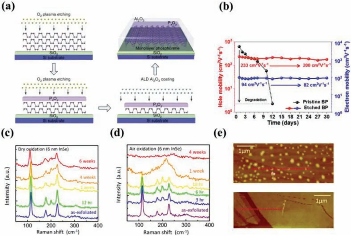
Fig.4.(a) Schematic diagram of the effects of the plasma treatment of a BP flake:thickness control, surface defect removal, and device fabrication process.Copied with permission [92].Copyright 2016, Nature Publishing Group.(b) Carrier mobilities of pristine BP FET and thermally etched BP FET as a function of exposure time under ambient condition.Copied with permission [95].Copyright 2018, American Chemical Society.(c, d) Time-dependent Raman specta of the 6 nm thick InSe flakes in dry oxidation and air oxidation.(e) AFM images of InSe surface after oxidation in air (top) and dry air (bottom).Copied with permission [28].Copyright 2017, American Chemical Society.
Althoughin-situoxidation encapsulation strategy overcomes the scalability limitations of mechanical transfer of h-BN, direct oxidation can easily generate a rough surface, for example, O2plasma left surface phosphorus oxide PxOyof several tens of nanometers thickness [55].Moreover, the plasma treatment typically requires technological expense and careful power optimization.Besides,insituoxidation perturbs the electronic structure of 2D materials,which is not suitable for some special electronic and optoelectronic applications.
2.5.Surface functionalization
The surface of 2D materials can be functionalized with various types of organic or inorganic nanomaterialsviacovalent and non-covalent bonding, which can be regard as another promising strategy for improving 2D materials stability and device performance for electronic and optoelectronic applications [99–104].Surface functionalization of 2D materials can not only create a barrier against the attack of oxygen/water in air, but also modulate the charge-transfer characteristic between 2D materials and functionalized components [105].Several kinds of encapsulation methodsviasurface functionalization of 2D materials are utilized to obtain an efficient and reliable encapsulation, including spin (or dip)-coating [106–110], drop-casting [111,112], vapor-deposition [113–115], self-assembly [116,117] and solution-based method [118–120],etc.
For the covalent functionalization methods, functional groups react with active chemical factors in 2D materials, such as the lone pair electrons in BP to form the P-X bonds [105], chalcogen atoms to be linked or chalcogen vacancies sites to be replaced for 2D metal chalcogenides [108,114,120].Covalent functionalization of 2D materials can be divided into two catalog, organic and inorganic molecules.For the organic covalent functionalization, several organic molecules had been utilized to enhance the stability of BP upon exposure to ambient conditionsviathe formation of covalent bonds, including P-C (C60 [121], aryl diazonium [122]), P-O-C (nucleophilic additions [123]), P-F (perfluorosulfonic acid [109]), P=N(4-azidobenzoic acid [124]), Ti-/Ln-P (titanium sulfonate ligand[120]),etc.Among these, using diazonium chemistry provides a robust approach for stabilizing 2D materials.Ryderet al.[122] have demonstrated an increased stability of BP against oxidative degradation for 3 weeksviacovalent functionalization with aryl diazonium compared with the unmodified BP nanosheets (Fig 5 a).The chemical modification of BP nanosheets by 4-nitrobenzenediazonium (4-NBD) and 4-methoxybenzene-diazonium (4-MBD)tetrafluoroborate salts resulted in a controllable p-type doping effect with an enhanced hole mobility and on/off ratio up to 106in FETs.Zhaoet al.[120] have demonstrated an excellent stability of BP during dispersion in water and exposure to air by surface coordination with titanium sulfonate ligand (TiL4, L referring to the sulfonic ester group), in which TiL4can coordinate with the BP lone-pair electrons.The chalcogen vacancies in TMDs crystal can not only act as active sites for O2or H2O adsorption resulting in degradation, but also for covalent bonding with organic groups to enhance their environmental stability.As an efficient encapsulation strategy, covalent functionalization with organic molecules have also been applied to improve the stabilities of TMDs for repairing their atomic vacancies, such as MoS(Se)2[106,108,125–127], WS(Se)2[114,128] and SnS2[110], which has been realized by using thiolated molecules like alkanethiol [125,127], perfluorodecanethiol (PFDT) [106] and thiophenol (PhSH) [114], poly (4-styrenesulfonate, PSS) [127], aryl diazonium [129] such as 4-NBD and 4-bromobenzene diazonium tetraborate (4-BBDT), nitrocellulose [108], ethylenediaminetetraacetic acid (EDTA) [110].Recently,Zhaoet al.[114] have reported that the monolayer WSe2surface containing Se vacancies can be functionalized by PhSH and the performance of WSe2transistors are improvedviadefect healing,which has been directly identified by scanning tunneling microscope (STM) imaging for the first time (Fig.5b).For the inorganic covalent functionalization, some inorganic molecules have been proved to efficiently stabilize 2D materials in ambient air, including metal and nonmetal elements, such as transition metals (Sc, Ti,V, Cr, Mn, Fe,etc.) [130] and Te [131], Se [132], NO2[133].Zhaoet al.[133] have demonstrated an air-stable chemical p doping on WSe2viacovalent bonding with surface absorbed NO2.A defectoriented model is proposed where NO2chemisorbs on WSe2surface and bulk defect sites (e.g., selenium vacancies), forming stable electron withdrawing WSe2-x-yOxNyspecies that lead to p-doping.Fig.5c depicts three distinct configurations with NOxchemisorption at the selenium vacancy sites:(i) WSe2:O, (ii) WSe2:NO2, (iii)WSe2:NO.
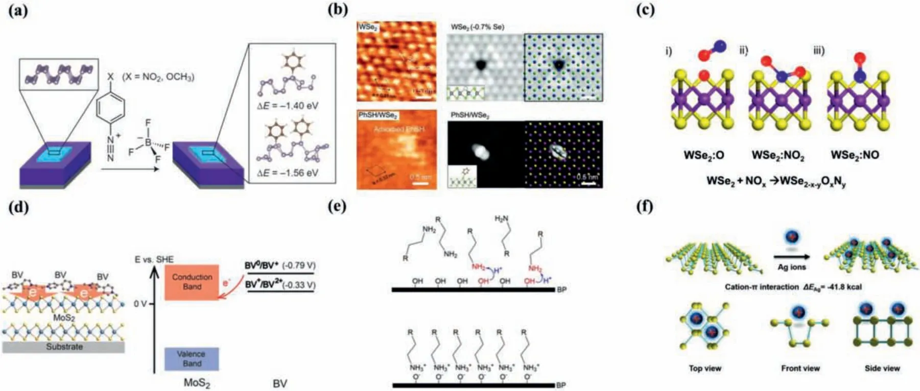
Fig.5.(a) Aryl diazonium functionalization of BP.Copied with permission [122].Copyright 2016, Nature Publishing Group.(b) PhSH functionalization of WSe2.Experimental and simulated scanning tunneling microscopic (STM) height image of the freshly exfoliated WSe2 surface with Se vacancy (top) and with the adsorption of thiophenol molecules (bottom).Copied with permission [114].Copyright 2020, John Wiley & Sons Ltd.(c) Schematic of NOx chemisorption at the selenium vacancy sites of WSe2 with three distinct configurations:(i) WSe2:O, (ii) WSe2:NO2, (iii) WSe2:NO.Copied with permission [133].Copyright 2014, American Chemical Society.(d) Schematic illustration of BV surface doping of MoS2 (Left).Energy band diagram of MoS2 and BV redox states (right).Copied with permission [111].Copyright 2014, American Chemical Society.(e) The mechanism of n-hexylamine coating on BP.Proton transfer takes place during the coating process (top) and then-hexylamine monolayer is formed on BP after the coating process is done (Bottom).R- in the diagram refers to C4H9- when representing hexylamine.Copied with permission [135].Copyright 2019, National Academy of Sciences.(f) Schematic illustrating adsorption of Ag+ on BP (top), three different views of the BP Ag+ structure (bottom).Copied with permission [119].Copyright 2017, John Wiley & Sons Ltd.
Noncovalent functionalization with organic and inorganic molecules is demonstrated to effectively enhance the stability of 2D materials against oxidization.Different reaction mechanisms of noncovalent functionalization of 2D materials involving electrostatic interactions, van der Waals interactions,and cation–πinteractions are described [134].Various organic molecules such asn-hexylamine [135], benzyl viologen (BV)[111,136,137], octadecyltrichlorosilane (OTS) [138–141], 7,7,8,8-tetracyano-p-quinodimethane (TCNQ) [112,142], 3,5,6-tetrafluoro-TCNQ (F4TCNQ) [143–147], triphenylphosphine (PPh3) [107,148],2,6,6-tetramethylpiperidinyl-N-oxyl (TEMPO) [149], perylenetetracarboxylicdianhydride (PTCDA) [115,150], perylenediimides (PDI)[151,152], bis(trifluoromethane) sulfonamide (TFSI) [118], dioctylbenzothienobenzothiophen (C8-BTBT) [153], imidazolium-based ionic liquids (ILs, [BMIM][PF6]) [154,155], phthalocyanine (Pc) compounds [113,156,157] have been reported to improve the stability of 2D materials.Kiriyaet al.[111] demonstrated that n-doped MoS2using BV as a surface charge transfer donor exhibited excellent stability in both ambient air and vacuum.As shown in Fig.5d, the neutral BV molecule (BV0) transfers electrons to the acceptor MoS2, and then formed BV molecule (BV2+).MoS2acts as an electron-acceptor material, and the BV0molecule can readily transfer electrons to MoS2.The good stability of this n-doped MoS2is attributed to the electron transfer complex formed by surface charge transfer between MoS2and BV.Recently, Suet al.[135] developed a strategy to effectively slow down the corrosion of BP by coating of alkylamine monolayer onto its surface (Fig.5e), leading to a prolonged lifetime for BP up to several weeks and even months in ambient air.They also demonstrated general applicability on a variety of other layered materials such as TMDs.In addition, thin layers selectively sifted out water molecules, forming a dry layer to achieve the passivation of the protected 2D materials.Beside organic molecules, noncovalent functionalization with inorganic metal-ion shows a desirable protection for BPviaweak cation-πinteractions [119].Guoet al.[119] utilized Ag+to interact with BP forming Ag+-functionalized BP to enhance both the stability and transistor performance of BP sheets, as shown in Fig.5f.After functionalization, BP can be preserved in humid air for 5 days and the Ag+-modified BP FET shows greatly enhanced hole mobility from 796 cm2V-1s-1to 1666 cm2V-1s-1and ON/OFF ratio from 5.9 × 10⁴to 2.6 × 10⁶.
Surface functionalization of 2D materials through covalent and non-covalent bonding with organic and inorganic components is a very promising technique for enhancing the stability of 2D materials, however, it also brings some restrictions or disadvantages to them.Covalent functionalization of 2D materials may largely change their intrinsic propertiesviastrong covalent bonding, such as the electrical and structural properties.In order to preserve their pristine properties to a great extent, noncovalent functionalization of 2D materials has been developed through weak interaction with 2D materials.Whereas, desorption and decomposition of functionalized moleculesvianoncovalent functionalization may occur easily on the surface of 2D materials, which is unstable for 2D materials encapsulation.
3.Encapsulation on 2D materials for device applications
Compared with 3D bulk materials, 2D materials are more vulnerable to environmental degradation due to their lager surface-tovolume ratio.Thus, achieving an air-stable and high-efficient devices based on 2D channel materials is significant important.In this section, we will focus on the encapsulation strategies of 2D materials in the applications of FETs and photodetectors devices.
3.1.Encapsulation on 2D materials for FET
As FETs transport channel material, the degradation of 2D materials under ambient conditions, not only increases the surface roughness but also leads to dopingviacharge transfer from the formed of chemical adsorbates oxygen or water, resulting in deteriorated performance of FETs based on 2D materials with low mobility, small current on/off ratio associated with large contact resistances and schottky barrier (SB) [158,159].Taking TMDs for example, the performance of MoS2devices can be strongly altered by environmental effects such as adsorbates, charges in neighboring dielectrics, and variability of contact quality [160,161].Leeet al.[32] reported h-BN sandwiched MoS2transistor exhibited no quality degradation (Fig.6a).The h-BN encapsulation provides excellent protection from environmental factors.Fig.6b shows that the h-BN encapsulated trilayer MoS2device experienced no electrical degradation after being stored in air for 4 months, even at elevated temperatures.The h-BN encapsulated devices showed almost no change in performance after cycling to 200 °C and back to room temperature, as shown in Fig.6c.In order to meet the requirements of FETs practical application in ambient air, more and more studies have reported that combination of encapsulation strategies improve the lifetime and performance of FETs.Honget al.[81] reported two-step encapsulation strategies to achieve n-doping effect and long-term stability in MoSe2FETs using oxygen plasma treatment followed by the deposition of an Al2O3layer (Fig.6d).Multilayer MoSe2FETs exhibited an enhancement in field-effect mobility from 12.23 cm2V-1s-1to 31.57 cm2V-1s-1and a 3 times higherIon/Ioff(Fig.6e), which may be attributed to the oxidation of topmost MoSe2to interfacial MoOxwith SeOxinduced by the oxygen plasma treatment, as well as to the existence of fixed positive charges in deposited Al2O3.In addition, the MoSe2FETs showed no sign of degradation under ambient conditions for 21 days (Fig.6f).Surface functionalization encapsulation strategy has been reported to induce surface doping in 2D materials, which can modulate the electronic properties of 2D materialsviainterfacial charge transfer, resulting in an improvement of the performance and stability of devices.Heoet al.[148] reported a highly stable and reversible n-doping technique for MoS2transistors based on charge transfer from PPh3(Fig.6g).After applying PPh3doping to the MoS2device, the energy band of the MoS2shifts downward due to the n-type doping transfers electrons to MoS2(Fig.6h).They explained that the effective barrier height (Φeff) and the tunneling barrier width for the electrons can decrease at the source/MoS2junction, thereby increasing the injection probability for electron carriers from the source to MoS2.After 14 days of air exposure, the PPh3-doped MoS2devices didnot show significant performance degradation in the transfer characteristic curves (Fig.6i), indicating that the PPh3doping exhibits excellent stability.
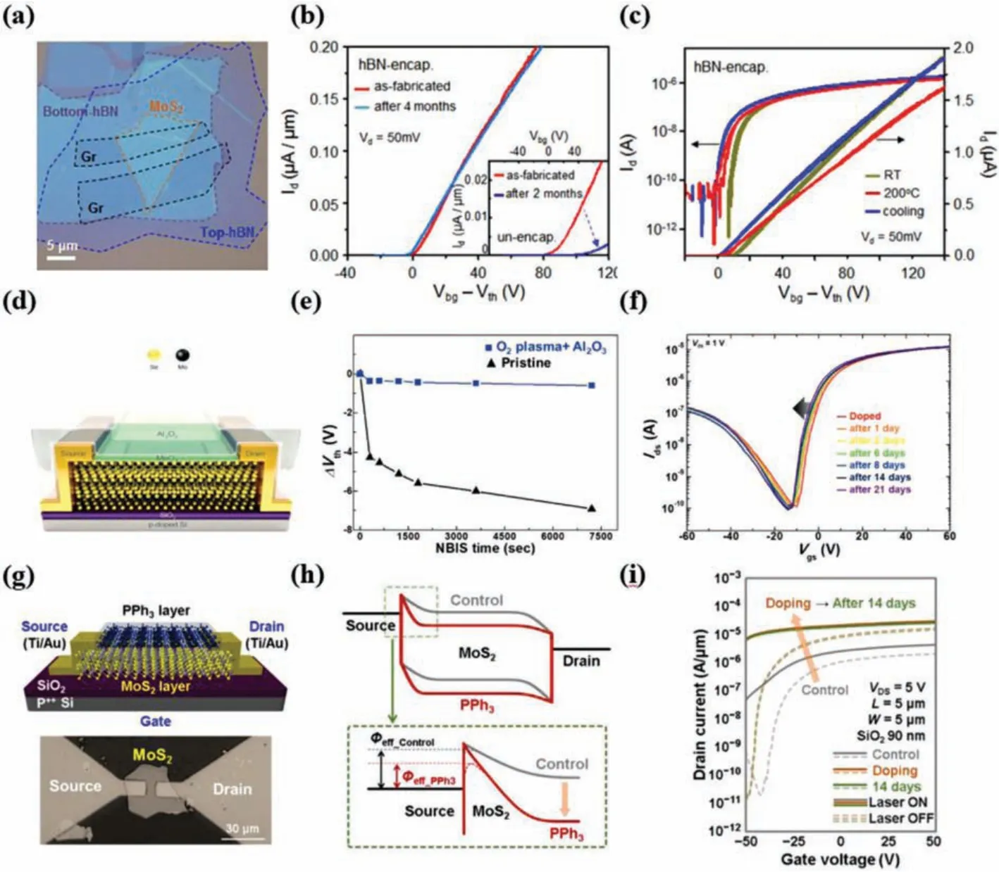
Fig.6.(a) Optical micrographs of a stack of hBN/Gr/MoS2/hBN before device fabrication.(b) Transfer curve of the hBN-encapsulated trilayer MoS2 device without degradation over 2 months, maintaining high performance.The inset shows the transfer curve of an unencapsulated trilayer MoS2 device.After 2 months, it shows a dramatic decrease of mobility from 7 cm2 V-1 s-1 to 1.2 cm2 V-1 s-1.(c) Transfer curves of the hBN-encapsulated trilayer MoS2 device operating at different temperatures.When the device was heated from room temperature to 200°C and then cooled, there is no performance degradation or change.Copied with permission [32].Copyright 2015, American Chemical Society.(d) A schematic of the doping process using O2 plasma treatment and Al2O3 passivation for the CVD-grown multilayer MoSe2 FET.(e) Comparisons of the shift in Vth derived from NBIS test results.(f) Environmental stability after three weeks in ambient air.Copied with permission [81].Copyright 2018, Wiley-VCH Verlag.(g) Schematic diagram and optical image of the PPh3-doped MoS2 transistor.(h) Energy band diagram of the source-TMD-drain junction before and after PPh3 doping.(i)Transfer characteristics of the control and PPh3-doped devices after 14 d of air exposure.Copied with permission [148].Copyright 2018, American Chemical Society.
3.2.Encapsulation on 2D materials for photodetectors
Degradation of 2D materials can dramatically affect the performance of photodetectors built on them, such as photoresponse(Rλ), response rate (τ), on/off ratio (Ion/Ioff), external quantum effi-ciency (EQE) [162].Liuet al.[43] demonstrated a graphene-BP heterostructure photodetector with ultrahigh responsivity and longterm stability at IR wavelengths.As shown in Fig.7a, the top layer of graphene functions not only as an encapsulation layer but also as a highly efficient transport layer.The graphene-BP heterostructure phototransistor exhibits a long-term photoresponse at nearinfrared wavelength (1550 nm) with an ultrahigh photoresponsivity (up to 3.3 × 10³A/W) (Fig.7b).In addition, the photoresponsivity of the graphene-BP device degraded approximately 6% after 60 days, suggesting excellent stability under ambient conditions (Fig.7c).As a presentative of the III-VI group materials, InSe is quite unstable and thin native oxide can easily form on the surface when exposed to an ambient environment, causing serious degradation of the device performance.Changet al.[93] presented an ultrahigh gain InSe-based photodetector by using a novel approach to modulate the carrier concentration of multilayered InSe semiconductor by controlling the formation of a surface oxide layerviaoxygen plasma treatment (Fig.7d).As shown schematically in Fig.7e, the built-in electric field caused by the formation of a carrier concentration gradient near the interface of oxide/InSe semiconductor heterostructures may thus result in the efficient photogenerated carrier separation under light illumination.The record high photoresponsivities of InSe-based photodetector with ~5 × 10⁶A/W at the excitation wavelength of 365 nm and 5 × 10⁵A/W at the wavelength of 530 nm can be obtained (Fig.7f).In addition to the charge transfer interaction with environmental species, organic molecules adsorbed on the surface of 2D materials can also induce charge transfer doping.We realized the ultrafast photoresponse dynamics in monolayer MoS2by combining non-covalent functionalization with surface-assembled zinc phthalocyanine (ZnPc) molecules and ALD Al2O3layer (Fig.7g)[163].After deposition of Al2O3layer, both the dark and light current of the ZnPc-treated MoS2devices are found to be significantly increased by a factor of 103to 105(Fig.7h), which are much larger than that of the initial CVD-grown MoS2.Such a dramatic enhancement is attributed to the effective screening of the charge impurity scattering in devices by both the increased electron concentration and the high-k dielectric passivation.This charge transfer promoted the photocarrier separation, reducing slow minority carrier trapping, and providing an accelerated responserate (80 ms) as shown in Fig.7i.
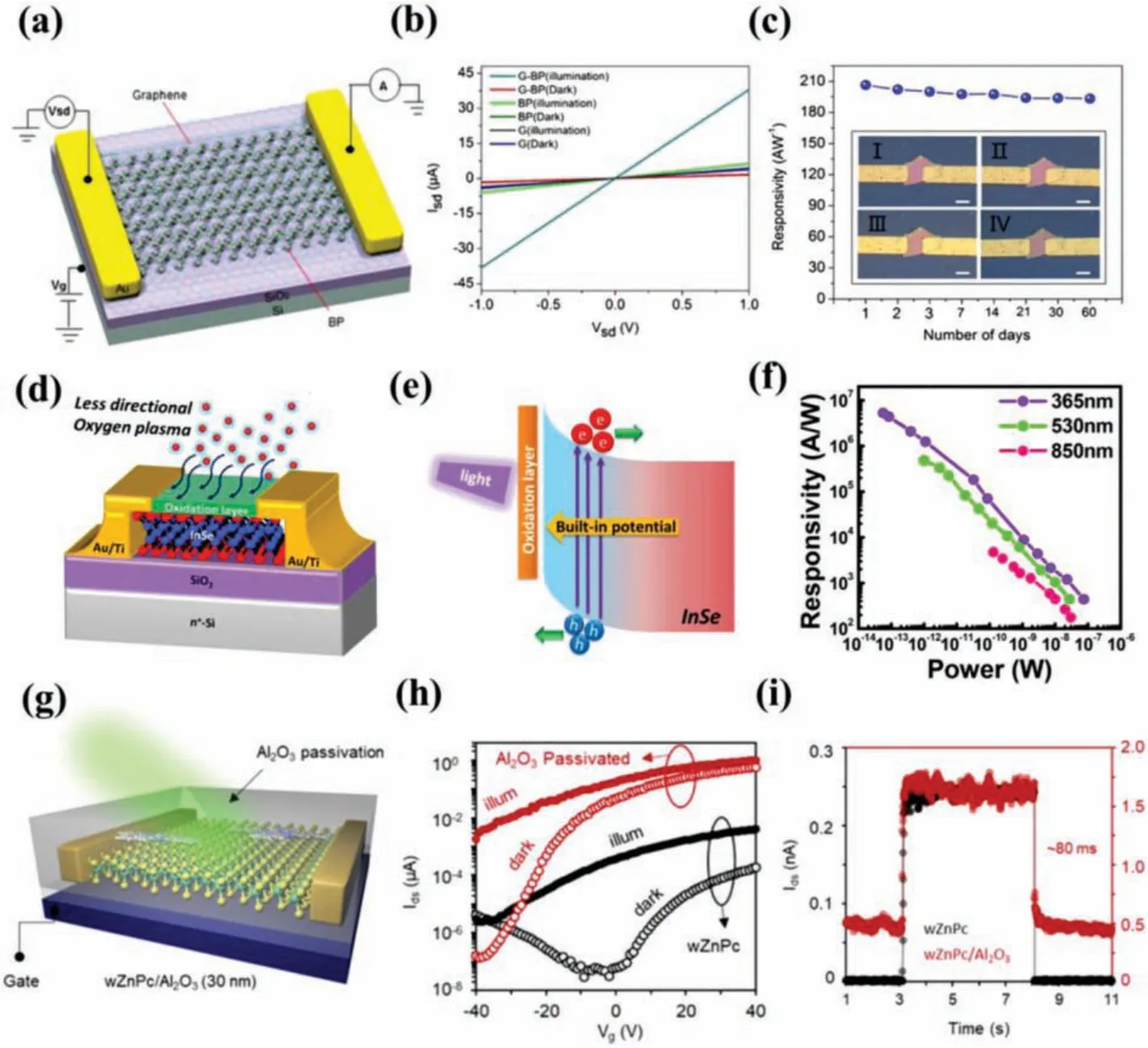
Fig.7.(a) Schematic diagram of the graphene-BP heterostructure photodetector.(b) I-V curves of the graphene-BP heterostructure, pure graphene, and pure BP photodetectors in the dark and under light illumination of 1550 nm wavelength.Vg = 0 V.(c) Responsivity of the graphene-BP photocurrent as a function of exposure time with a laser power of 211 nW; the thickness of the graphene-BP heterostructure is 35 nm.Inset:Optical images of the graphene-BP heterostructure photodetector as a function of time(I:1 day, II:7 days, III:30 days, and IV:60 days; all scale bars are 8 μm).The device characterization was performed in air at room temperature.Copied with permission[43].Copyright 2017, American Chemical Society.(d) Schematic representation of indirect incident plasma treatment on InSe photodetector.(e) Schematic representation of charge separation enhancement mechanism.(f) Photoresponsivities of InSe photodetector treated with indirect incident plasma treatment for 10 s at different illumination wavelengths.Copied with permission [93].Copyright 2017, American Chemical Society.(g) Schematic of a ZnPc-decorated MoS2 photodetector with top Al2O3 encapsulation.The transfer curves and transient photoresponse characteristic of the device before and after the Al2O3 encapsulation are displayed in (h) and (i).Copied with permission[163].Copyright 2018, American Chemical Society.
4.Summary and outlook
Over the past decade, atomically thin 2D materials have been used as building blocks for electronic and optoelectronic applications owing to their fascinating optical and electronic properties.However, a fundamental obstacle impeding the application of 2D materials is their instability under ambient conditions.Thus,searching effective encapsulation strategies based on 2D materials to achieve stable and high-performance devices encounter great challenges.In this review, we focused on the recent progress ofthe encapsulation strategies for improving 2D materials stability against environmental degradation including mechanical transfer, polymer coating, film deposition,in-situoxidation and surface functionalization.Depending on different encapsulation strategies, they have shown different effectiveness.Mechanical transfer of other stable 2D materials have been proved to be a useful strategy to protect 2D materials, but it requires harsh preparation conditions and complicated technologies.Polymer coatings is an easy and low-cost method, which can isolate 2D materials from environmental active substances, however, a major issue that hightemperature tolerance should be considered, which would impede their device applications.Encapsulation with ALD oxides is good for long-term stability and has been applied in large-scale preparations.However, defects and impurities introduced by this encapsulation method could hinder the carrier transport in 2D materials.In-situoxidation is an effective way that oxygen atoms can spontaneously blend into the 2D materials surface to form oxide layers.Nevertheless, this method is very easy to lead to p-doping of 2D materials, thus limiting its specific use.Surface functionalization through covalent or noncovalent approach using organic and inorganic molecules, which has been proved to be a useful strategy to protect 2D materials, however, functionalized surfaces are also obtained at the same time, which can break original electronic properties of 2D materials, thus limit its application in certain occasions.Currently, extensive effects have been made on the encapsulation of 2D materials in electronic and optoelectronic applications, using these strategies individually or in combination provides a great platform for long-term stable and high-performance devices.
Although great progress has been made on the encapsulation of 2D materials, it is still in the sprouting stage to improve the performances for further practical applications.There are several challenges and opportunities to be resolved.(I) Degradation chemistry for each material is different due to their diverse chemical structure.Moreover, degradation mechanism for most 2D materials is still unclear.For example, the key role of illumination to initiate BP oxidation is still in debate.Hence, more experimental and theoretical studies are needed to get an in-depth insight of the degradation mechanism of 2D materials in ambient condition, if we want to achieve long-term stable 2D materials over months or years.(II)In addition to passivate 2D materials, in fact, in most cases, encapsulation materials can interaction with 2D materials to form heterojunctions or functionalize them, which could influence the interface electronic structure and charge transport.Thus, many fundamental issues must be considered, such as surface charge transfer doping and carriers transport between them [164].Besides, unpredictable and troublesome problems are induced from the low glass transition temperature for surface functionalization with organic molecules, such as hardening.(III) Defects play a key role in determining the stability of 2D materials when exposed to an ambient environment.Moreover, wafer-scale 2D semiconductors are beneficial to the modern microelectronic devices integration [6].Therefore, it is urgent to find new and stable 2D family members and develop wafer-scale with less defects growth approaches.
Declaration of competing interest
The authors declare no conflict of interest.
Acknowledgments
This work was supported by the National Natural Science Foundation of China (Nos.21825103, 51902227 and 11574241), and the Open Project of State Key Laboratory of Materials Processing and Die & Mould Technology, Huazhong University of Science and Technology, China (No.P2020-021).
 Chinese Chemical Letters2022年5期
- Chinese Chemical Letters的其它文章
- Recent advances in enhancing reactive oxygen species based chemodynamic therapy
- An integrative review on the applications of 3D printing in the field of in vitro diagnostics
- Recent developments of droplets-based microfluidics for bacterial analysis
- Dynamics and biological relevance of epigenetic N6-methyladenine DNA modification in eukaryotic cells
- Recent progress in advanced core-shell metal-based catalysts for electrochemical carbon dioxide reduction
- Recent advances in carbon-based materials for electrochemical CO2 reduction reaction