Design of a Microwave Filter Based on a Novel Negative Coupling Structure with Conical Through-Hole
Shunliang Meng,Fei Liang,2,*,Wenzhong Lu,2,Zihang Lin,Yuhao Yin,Rong Zhang
1 School of Optical and Electronic Information,Huazhong University of Science and Technology,Wuhan,430074,China
2 Wenzhou Advanced Manufacturing Institute,Huazhong University of Science and Technology,Wenzhou,325000,China
Abstract: This article introduces the design theory of ceramic waveguide filter and proposes a new type of negative coupling structure with a conical throughhole, which has fine-adjustment of negative coupling without significantly increasing the insertion loss of the filter.Based on this,the article proposes an eightcavity ceramic waveguide filter design for 5G base stations.It also presents a detailed discussion on the influence of the cross-coupling slot lengths L2 and L4 on the transmission zeros positions during the filter optimization process and the relevant change rules.For the proposed optimized filter, the observed performance indicators include the center frequency of 3.5 GHz,working bandwidth of 200 MHz,an insertion loss of ≤2.0 dB,return loss of ≥19 dB,and out-of-band nearend suppression and out-of-band far-end suppression of ≥39 dB and ≥63 dB,respectively.The test performance results obtained for the sample,with structural parameters as per the simulation model,were in good agreement with the simulation results.
Keywords: ceramic waveguide filter; negative coupling structure; out-of-band suppression characteristics;cross-coupling slot
I.INTRODUCTION
The rapid development of fifth-generation communication technology has created a significant demand for base station filters, for the communication systems,with small size, lightweight, high performance, and low cost.The most popular choice of base station fliters in the 2G,3G,and 4G communication systems are metal coaxial cavity fliters with volume and mass too large to meet the miniaturization and lightweight requirements of 5G base stations.Further, microwave ceramic waveguide fliters are the mainstream choice of fliters for 5G base stations due to their unique advantages of small size,low loss,and good thermal stability[1–6].Therefore,the study of high-performance ceramic waveguide fliters has become crucial for scientifci endeavors and practical application prospects.
For the ceramic waveguide filter, the negative coupling structure design achieves capacitive coupling and introduces transmission zeros.A widely used negative coupling structure is the blind hole negative coupling structure proposed by Huawei Bengui Yuan.This structure has a simple design but achieving the fine-adjustment of a small coupling amount is not easy[7].Other typical negative coupling structures include the step through-hole negative coupling structure with metal coating notch proposed by ZTE Wei Bu [8]and the microstrip negative coupling structure recently proposed by Zhengjun Du [9], with both achieving capacitive coupling but both having obvious electromagnetic leakage problems, which can increase the insertion loss of the filter.The abovementioned negative coupling structures have found wide applications in the structural design of capacitive coupling in ceramic waveguide filters but with associated problems including debugging difficulties and high electromagnetic radiation coupling which is non-conducive for the development of high-performance ceramic waveguide filters.
This paper proposes a new type of negative coupling structure that can achieve capacitive coupling.The negative coupling structure contains a cylindrical hole and a conical hole.Change in the cylindrical hole depth and the metal coating area of the conical hole leads to fine-adjustment of the negative coupling amount,and the notch position adjustment in the metal coating layer of the conical hole reduces the radiation loss.The filter topology has a designed double CQ structure,which can produce two pairs of transmission zeros.Change in the lengths L2 and L4 of the crosscoupling slot and the relative position offset P1 of the negative coupling structure provides relatively independent position-adjustment of the two pairs of transmission zeros for suppressing the near and far end of the filter passband simultaneously and thereby, meeting the application requirements of high out-of-band suppression scenarios.Thus, this study proposes an eight-cavity ceramic waveguide filter designed based on the above-discussed new negative coupling structure and topology.After repeated optimizations and adjustments, the eight-cavity ceramic waveguide filter meets the performance requirements,leading to the corresponding sample preparation.The test results indicate that the test results are in good agreement with the simulation results.
II.FILTER DESIGN
The filter,a frequency selective device,forms a working passband by mutual coupling between multiple resonant cavities and realizes signal transmission through input and output ports.This paper presents the ceramic waveguide filter design based on the parameter methods of cavity resonance frequency,interstage coupling bandwidth,and external quality factor.The inter-stage coupling bandwidth and the external quality factor quantitatively calculate the coupling between the resonant cavities and the coupling and the resonant cavity and the port, respectively.The calculation formulas for the inter-stage coupling bandwidth and external quality factor of the resonant cavity are as follows:
Among them,f2andf1represent the upper and lower resonant frequency of the coupled resonant cavity,respectively;Qerepresents the Q value calculated by the terminal resistance reflected the first resonant cavity,τmaxis the maximum group delay,andω0is the maximum group delay corresponding angular frequency[10,11].
2.1 Design of Negative Coupling Structure and Feed Structure
Figure 1a,1b,and 1c depict the proposed new negative coupling structure with a conical through-hole.The negative coupling structure contains a cylindrical and a conical hole in the respective upper and lower part.The inner wall of the cylindrical through-hole and a part of the inner wall of the conical through-hole have metal-coating.The realization of coupling adjustment is through changing the cylindrical hole depth and the metal coating area in the conical hole, which has a higher degree of freedom and can meet the small coupling requirements.Besides,opening the metal notch of the conical through-hole the weak electromagnetic field distribution area leads to device radiation loss reduction in the structural design.This article comprehensively considers three kinds of design schemes corresponding to the metal notch at different positions of the conical hole,including the metal notch at the bottom, the top, and the middle area of the conical hole.Figure 1a,1b,and 1c illustrate the sectional drawings of all the three design schemes.
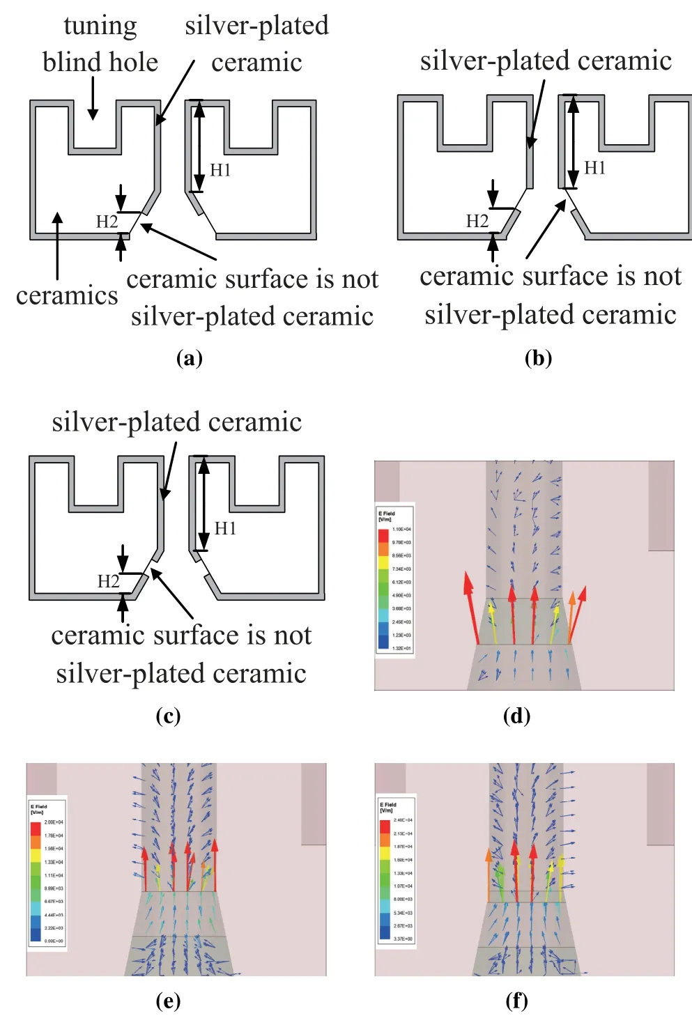
Figure 1. a, b and c are the respective sectional views of the metal notch at the bottom,top,and middle of the conical through-hole negative coupling structure.d,e,and f are the respective electric field distribution diagrams for the metal notch at the bottom,top,and middle of the conical throughhole negative coupling structure.
The simulation software HFSS is used to analyze the electric field distribution of the conical-through hole.Figure 1d, 1e, and 1f depict the electric field distribution,respectively,for the notch area at the bottom, top, and middle of the conical hole.According to the electric-field distribution diagram, the electricfield energy concentration in the conical through-hole is on the metal coating and the metal notch area boundary.For the notch area located at the bottom of the conical hole,adjusting the depth of the cylindrical hole on the upper part of the through-hole has little influence on the electric field distribution,and the coupling bandwidth changes gently with H1.For the notch area at the top or middle of the conical hole, adjusting cylindrical hole depth on the upper part of the through-hole influences the electric field distribution significantly and increases the coupling bandwidth to H1,which is non-conducive to the design and debugging of the filter coupling structure.
Figure 2 shows the relationship between the negative coupling bandwidth of the three design schemes and the structural parameter H1.For the notch area at the bottom of the conical hole, the negative coupling structure debugging is between 0 to -250MHz through the change in the metal coating area, which fulfills the designing requirements of the negative coupling of the ceramic waveguide filter.However, this makes the other two schemes are hard to achieve.Figure 3 shows the relationship between the negative coupling bandwidth of all the three design schemes and the structural parameter H2.Thus, the best design scheme for the negative coupling structure is opening the metal notch at the bottom of the conical hole.With this scheme, change in metal coating area of the conical hole and the cylindrical hole depth causes rough and fine-adjustment of the negative coupling amount,respectively.
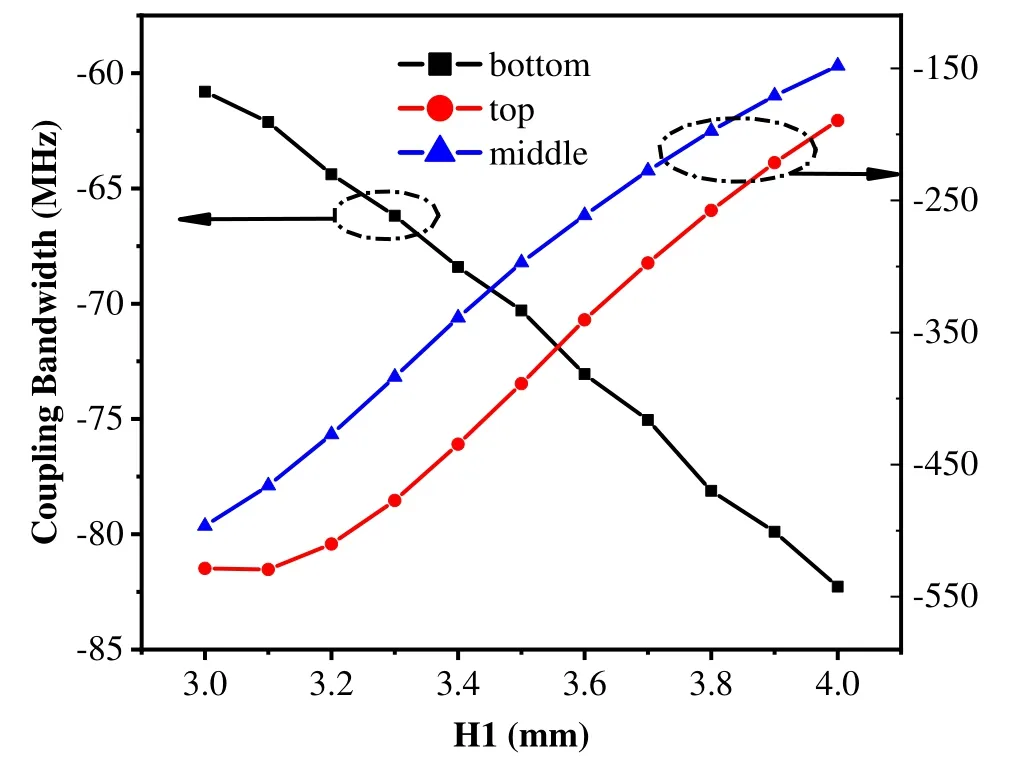
Figure 2. The curve for the coupling amount of the conical through-hole negative coupling structure changing with H1.
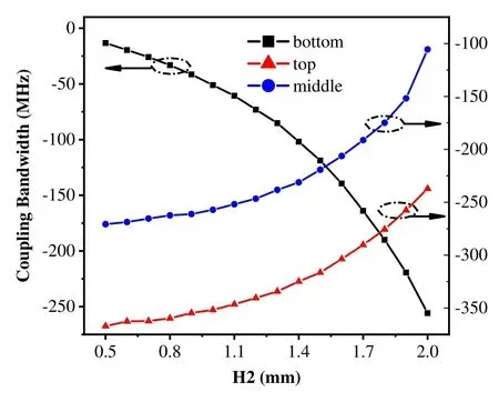
Figure 3. The coupling amount curve for the conical through-hole negative coupling structure changing with H2.
With the structure parameter size accuracy of 0.1 mm, the debugging accuracy of negative coupling of conical through-hole is nearly 2 MHz.The subsequent proposed design of the ceramic waveguide filter adopts the afore-discussed design.Compared with the microstrip negative coupling structure, the gap of metal coating in the microstrip negative coupling structure is located in the region with strong electromagnetic field distribution, while the metal coating gap of conical through-hole structure is located in the weak area of electromagnetic field distribution,thus effectively reducing the electromagnetic radiation of the filter and reducing insertion loss; At the same time, the change of the structure parameters of the microstrip structure will have a great impact on the electromagnetic field distribution,which will increase the difficulty of the optimization of the structure parameters;while the change of the structure parameters of the conical through-hole structure has a relatively small impact on the electromagnetic field distribution,and the debugging accuracy of the coupling bandwidth can reach 2MHz, which effectively reduces the difficulty of the design and debugging.The third section analyses the influence of the radiation loss,due to the metal notch area of the conical through-hole, on the insertion loss of the filter.Besides, the signals feed mode of the ceramic waveguide filter is probe feed.The feed-depth change of the probe effectively adjusts the coupling strength between the port and the resonator.Figure 4 depicts the structure model and the parameter curve.
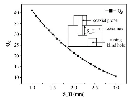
Figure 4.The relationship curve between the external quality factor and feed depth for the probe feed model.
2.2 Design of Eight-Cavity Ceramic Waveguide Filter
This article proposes an eight-cavity ceramic waveguide filter design, based on the above-discussed design theory,which can achieve adjustable out-of-band suppression characteristics and fulfill stringent out-ofband suppression requirements.It can also meet the technical index requirements of ceramic filters, used in the 5G base stations of giant communications technology companies.The following are specification requirements, including filter center frequency of 3.5 GHz,working bandwidth of 200 MHz,a return loss of≥17 dB,an insertion loss of≤2.0 dB,stopband suppression of≥38 dB for 3.3–3.36 GHz and 3.64–3.7 GHz, the stopband rejection of≥62 dB for 3.2–3.3 GHz and 3.7–3.8 GHz frequency band,and the group delay in the passband is≤20 ns.
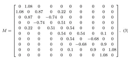
This paper proposes an eight-cavity ceramic waveguide filter design, fulfilling the target requirements,with double CQ structure, which has capacitive coupling between cavities 2 and 3, capacitive coupling between cavities 6 and 7, and inductive coupling between the others.It forms two CQ cells with capacitive cross-coupling and introduces two pairs of the transmission zeros for further improving the out-of-band suppression of the filter [12, 13].As per the technical requirements and filter topological structure, the parameters of the theoretical model of eight-cavity ceramic waveguide filters, such as cavity resonant frequency, inter-stage coupling bandwidth, and external quality factor,are determined by the filter design software.Table 1 depicts these afore-mentioned parameters, where frequency represents the cavity resonance frequency,CBWnmrepresents the inter-stage coupling bandwidth of the cavity,the numerical subscript represents the cavity, andQS1andQ8Lrepresent the external quality factor.
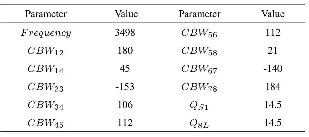
Table 1. Relevant theoretical model parameters(in MHz).
Formula(3) and Figure 5 show the coupling matrix and topological structure of the eight-cavity ceramic waveguide filter, respectively.Figure 6 is the structural diagram of the eight-cavity ceramic waveguide filter designed as per the topological structure and theoretical parameters.This study first establishes the single cavity ceramic waveguide resonator model in HFSS software, as per the relevant theoretical model parameters,and then calculates the resonant frequency of the single cavity by the eigenmode method.It determines the tuning blind hole depth,which is the basis for establishing the coupling structure model of the eight-cavity ceramic waveguide filter.Further, the Ymatrix method performs the coupling bandwidth calculations for resonators and determines each coupling structure parameter.Lastly, by establishing the feed structure model of the filter, the group delay method calculates the external quality factor and determines the feed structure parameters.
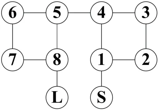
Figure 5. The topology of the eight-cavity ceramic waveguide filter.
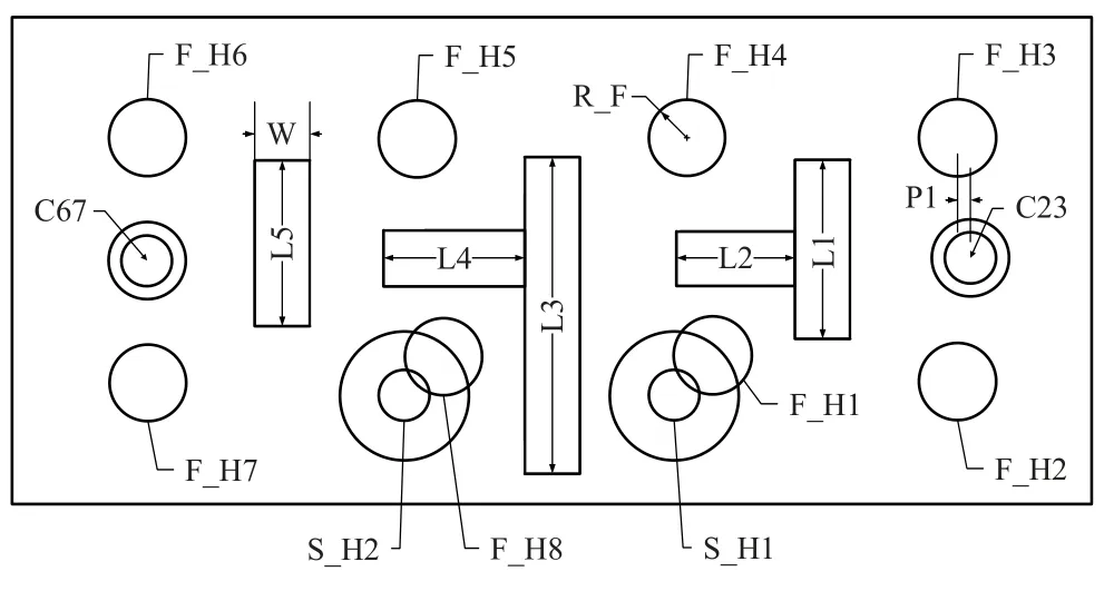
Figure 6.Structure of eight-cavity ceramic waveguide filter.
The filter curve obtained, as per the initial value of the filter structure parameters calculated,is dissimilar to the ideal filter curve.It necessitates further optimize the filter structure parameters.Thus,for achieving the best filtering characteristics, optimization of the filter structure parameters is by the parameter extraction method.This paper first determines the error distribution between the simulation model and the theoretical model during the parameter extraction process.According to the error distribution,continuous optimization of the filter structure parameters, such as tuning blind hole and coupling structure,reduces the parameter error between the simulation model and the theoretical model and achieves consistency between the simulation model and the theoretical model at last.
III.SIMULATION AND TEST OF FILTER
3.1 Simulation and Optimization of Filter
Figure 7 depicts the analysis and comparison of radiation loss influence of conical through-hole negative coupling structure on filter insertion loss.For this analysis, the|S21|curves of eight-cavity ceramic waveguide filters designed by Huawei blind hole negative coupling structure (patent example 1) [7] and ZTE stepped through-hole negative coupling structure(patent example 1) [8] are simulated and compared with the conical through-hole negative coupling structure.It revealed that the insertion loss of the ceramic waveguide filter, with conical through-hole, is slightly higher and lower than the ceramic waveguide filter with blind-hole and stepped through-hole, respectively, without considering the ceramic dielectric loss and surface metal conductor loss.
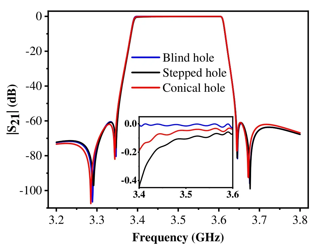
Figure 7. |S21| curves of an eight-cavity ceramic waveguide filter designed with three negative coupling structures.
As per the analysis, the difference between the average insertion loss of the passband of the conical through-hole and the blind hole structure filter is only 0.05 dB.The filtering characteristics of the filters designed by the two negative coupling structures are almost identical,and the difference between the average insertion loss of the passband of the stepped throughhole and the blind hole structure filter is 0.13 dB.Besides, the radiation losses are much lower for the negative-coupling structure with the conical throughhole than the stepped through-hole structure.The proposed conical through-hole negative coupling structure has higher debugging accuracy than the blindhole negative coupling structure and a lower radiation loss than the stepped through-hole negative coupling structure.Thus, it has strong practicability and can fulfill the design requirements of a high-performance ceramic waveguide filter.
The realization of out-of-band suppression adjustment in the ceramic waveguide filter is by changing the transmission zero positions.The eight-cavity ceramic waveguide filter designed in the study introduces two pairs of transmission zeros.The position adjustment of transmission zeros at the near-end and far-end of the passband realizes respective out-of-band suppression at the near-end and far-end.The simulation results depict that, at the near-end of the passband, the cross-coupling slot length L2 between cavities 1 and 4 controls the positions of a pair of transmission zeros.With L2 increases, the transmission zeros at the near end of the passband move far from the working passband, and when L2 decreases, the transmission zeros at the near-end move closer to the working passband.The cross-coupling slot length L4 for cavities 5 and 8 controls the positions of a pair of transmission zeros at the far-end of the passband.The change rules in the positioning of the transmission zeros at the far-end of the passband with L4 is similar to the change rules of the positioning of zeros at the near-end of the passband with L2.Thus,the two pairs of transmission zeros positions are relatively independent and adjustable,with good freedom of debugging,easy production,and processing debugging.Figure 8 and 9 depict the relationship curves of the filter|S21|with L2 and L4,respectively.
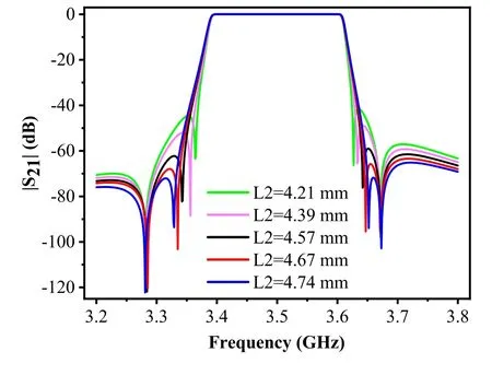
Figure 8. Graph of the relationship between |S21| and L2 of the filter.
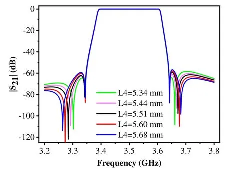
Figure 9. Graph of the relationship between the filter|S21|and L4.
Both changes in the length of L2 and improvement of the transmission curve symmetry near the filter passband can achieve the near-end suppression in the eight-cavity ceramic waveguide filter.Further, simulation analysis found that the near-end transmission curve symmetry of the working passband is closely related to the relative position offset P1 of the negative coupling structure between the cavities 2 and 3.The relative position offset P1 is according to the center position of the blind tuning hole of cavities 2 and 3.If P1 is a negative number,it implies a left shift in the negative coupling structure,and a positive P1 number indicates a right-shift in the negative coupling structure.With P1<0, the position of the pair of transmission zeros at the near-end shifts to the left in the low-frequency direction.With P1>0 and within a specific range, the transmission zeros position shifts to the right.The simulation results show that when P1=0.5 mm,the transmission curve is symmetrical at the near-end,and the near-end out-of-band rejection of the filter improves significantly.Figure 10 shows the relationship curve of filter|S21|with P1.
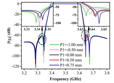
Figure 10. Relationship curve diagram of the filter |S21|with P1.
3.2 Simulation and Performance Test of Filter
Simulation provides the best filtering characteristics of the eight-cavity ceramic waveguide filter by repeated optimization of the structural filter parameters.Figure 11 depicts the simulation model.The relative dielectric constant of the ceramic material is 23.1, the overall size of the model is 42×19×6mm3, and the other details of structure parameters are in Table 2.Figure 13 and Figure 14 depict the simulation curves,with the center frequency of the filter at 3.5 GHz,the working passband at 200 MHz,the return loss of≥23 dB,the stopband rejection of≥39.7 dB and≥62 dB for 3.3–3.36 GHz and 3.64–3.7 GHz frequency band and of 3.2–3.3 GHz and 3.7–3.8 GHz frequency band,respectively,and the group delay of simulation model at 3.4-3.6 GHz is≤20 ns.It can be seen from Figure 13 that the coupling matrix is in good agreement with the simulation results,but there is a slight deviation in the positions of the transmission zeros between the two.This is mainly because the coupling coefficient of the coupling matrix is an ideal value and does not change with frequency.However,the coupling coefficient corresponding to the actual coupling structure will change with the change of frequency.In addition,the frequency response of the two in the passband also has a slight deviation,which is mainly because the simulation model does not consider the dielectric loss and the conductor loss, but the Q value of the filter corresponding to the coupling matrix is a finite value.
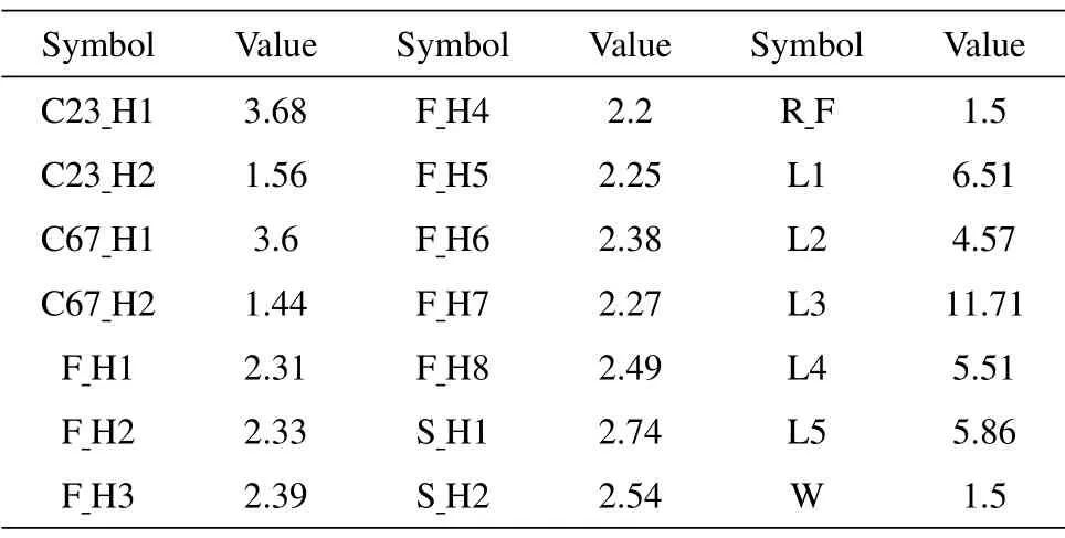
Table 2. Structural parameters of the eight-cavity ceramic waveguide filter(in mm).
Figure 12 shows the prepared ceramic waveguide filter sample following the structural parameters of the simulation model.Figure 13 and Figure 14 show the performance curve of the filter sample tested by the vector network analyzer E5063A.According to the curve, the center frequency of the filter sample is 3.5 GHz,the working passband is 200 MHz,return loss is≥19 dB,insertion loss is≤2.0 dB,stopband suppression for 3.3–3.36 GHz and 3.64–3.7 GHz frequency bands is≥39 dB, stopband suppression for 3.2–3.3 GHz and 3.7–3.8 GHz frequency bands is≥63 dB,and the group delay obtained by the sample test at 3.4-3.6 GHz is≤19.8 ns.Thus,all performance indicators have reached the expected target requirements.
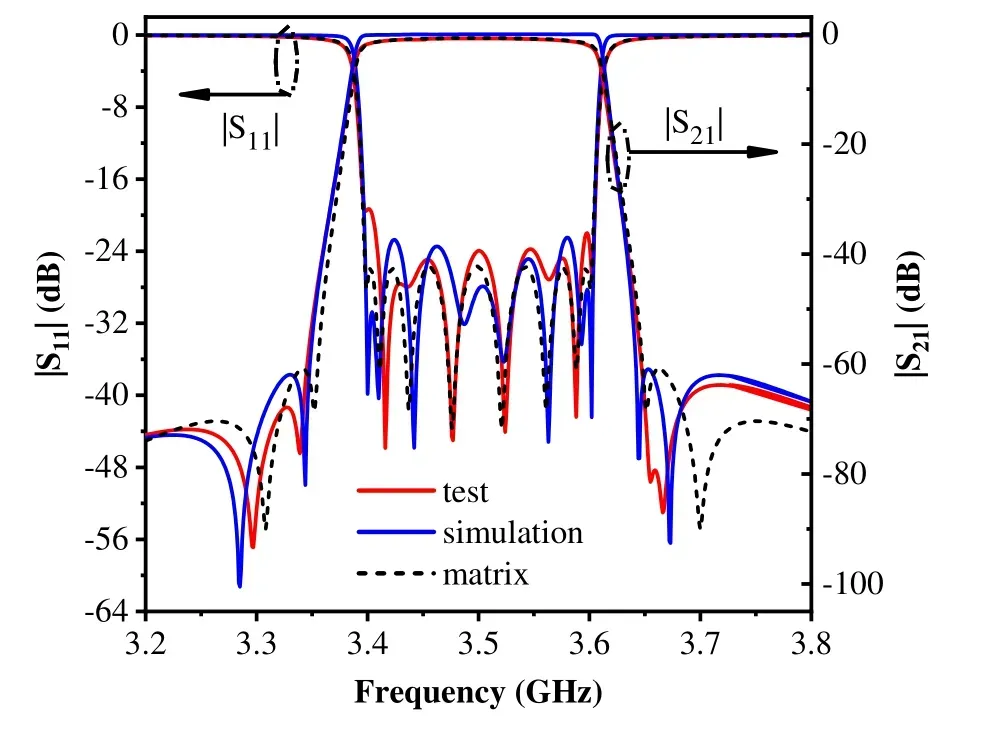
Figure 13. Matrix, simulation and test curves of eightcavity ceramic waveguide filter.
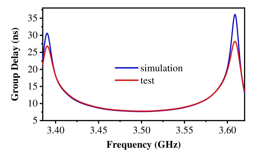
Figure 14. The group delay of eight-cavity ceramic waveguide filter.
The simulation results and test results for the filter are consistent,which verifies the design feasibility.However, there are differences in the passband return loss and the out-of-band suppression of the stopband.It is mainly due to the theoretical calculation errors in the simulation model, the dimensional control inaccuracy during the ceramic preparation process, and the silver layer etching in the performance debugging stage.The HFSS simulation model has ideal the dielectric constant and loss of ceramic materials,but the microwave dielectric properties for the actual ceramic materials are non-ideal.Further,the structural parameters of ceramic waveguide filters have high dimensional accuracy requirements, but there is a specific gap between the actual production and processing accuracy and the target requirement.During the performance testing and debugging stage,a part of the silverlayer etched on the ceramic surface optimizes the filter curve and causes a specific error.The eight-cavity ceramic filter sample has a large passband insertion loss as compared to the simulation model.It can be due to the increase in the number of cavities, the increase in the dielectric loss, and conductor loss of the filter.However, the silver layer etching on the ceramic surface during the performance testing and debugging of the ceramic filter could cause additional radiation loss.Further,the simulation model does not consider the dielectric loss of the filter, the conductor loss, and the radiation loss caused by the silver layer etching on the ceramic surface.Thus, the insertion loss of the filter sample is relatively higher than the simulation model.
Table 3 compares the performance difference between the eight-cavity ceramic waveguide filter and the current base station filters.From the comparison,it can be seen that the eight-cavity ceramic waveguide filter has the unique advantages of small volume and high out-of-band suppression,which can meet the requirements of lightweight and high performance of 5G base station filter,and has a good application prospect.
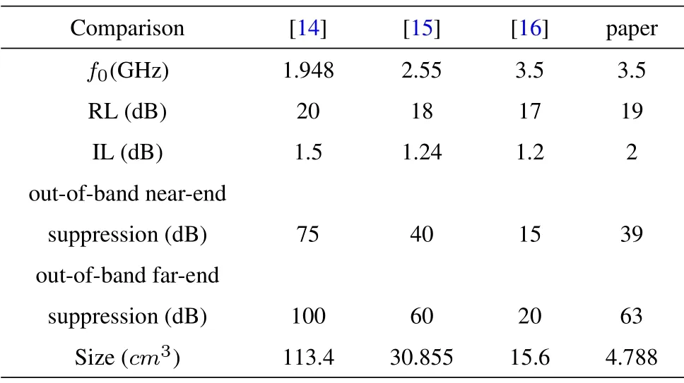
Table 3. Performance comparison between eight-cavity ceramic waveguide filter and current base station filters.
IV.CONCLUSION
This article proposes a new type of negative coupling structure with a conical through-hole.Change in the cylindrical hole depth and the metal coating area of the conical hole realizes fine-adjustment of negative coupling.The adjustment accuracy for the coupling bandwidth of the negative coupling structure is nearly 2 MHz, with the average radiation loss in the passband of only 0.05 dB, which can meet the design requirements for the high-performance ceramic waveguide filters.In topological terms of filter designing,by changing the cross-coupling slot length L2 and L4,two pairs of transmission zeros can be independently adjusted to effectively control the respective out-ofband suppression of the near-end and the far-end of the passband.The results depict that the cross-coupling slot length L2 control the positions of a pair of transmission zeros near the passband.When L2 increases,the transmission zeros at the near-end of the passband are far from the working passband, and when L2 decreases, the transmission zeros at the near-end are closer to the working passband.The length L4 of the cross-coupling slot controls a pair of transmission zeros at the far-end of the passband.The variation of the transmission zeros at the far end of the passband with L4 is similar to that at the near end of the passband with L2.In addition, it is found that by adjusting the offset P1 of the relative position of the negative coupling structure,the symmetry of the nearend transmission curve of the working passband can be improved, which further improves the out-of-band suppression characteristics of the filter.When P1<0, a pair of transmission zeros move left in the direction of low frequency, and when P1>0 and within a particular range,the transmission zeros move to the right.The designed eight-cavity ceramic waveguide filter has the benefits of simple structure,lightweight,and excellent performance.It fulfills the performance requirements of the 5G base station microwave filter and has good application prospects.
ACKNOWLEDGEMENT
This work was supported by the National Natural Science Fund Joint Fund Project (No.U21B2068), and the Major Science and Technology Innovation Project of WenZhou(No.ZG2021014).
- China Communications的其它文章
- A User-Friendly SSVEP-Based BCI Using Imperceptible Phase-Coded Flickers at 60Hz
- Steady-State Visual Evoked Potential(SSVEP)in a New Paradigm Containing Dynamic Fixation Points
- Toward a Neurophysiological Measure of Image Quality Perception Based on Algebraic Topology Analysis
- Transfer Learning Algorithm Design for Feature Transfer Problem in Motor Imagery Brain-computer Interface
- Removal of Ocular Artifacts from Electroencephalo-Graph by Improving Variational Mode Decomposition
- BCI+VR Rehabilitation Design of Closed-Loop Motor Imagery Based on the Degree of Drug Addiction

