A DFT study of the effect of stacking on the quantum capacitance of bilayer graphene materials
CUI Guang-yu, YI Zong-lin, SU Fang-yuan,*, CHEN Cheng-meng,3, HAN Pei-de,*
(1. College of Material Science and Engineering, Taiyuan University of Technology, Taiyuan 030001, China;2. Key Laboratory of Carbon Materials, Institute of Coal Chemistry, Chinese Academy of Sciences, Taiyuan 030001, China;3. Center of Materials Science and Optoelectronics Engineering, University of Chinese Academy of Sciences, Beijing 100049, China)
Abstract: Graphene is acknowledged as one of the ideal active electrode materials for electric double-layer capacitors because of its extremely high specific surface area and outstanding electronic conductivity. By introducing defects or heteroatoms into the graphene sheet, the electronic structure around the defects can be altered, which could lead to an increased quantum capacitance (CQ)and therefore te capacitive performance. One of the unavoidable problems for manufacturing and using graphene materials is that the stacking of the layers affects their electronic structure, and eventually their capacitance. DFT calculations were used to investigate the effect of layer stacking in bilayer graphene materials on CQ and the surface charge density. A two layer, AB-stacked graphene model,in which the top layer is defective and the bottom one is perfect was assumed for the calculations. The defective graphenes investigated are those containing Stone-Thrower-Wales defects, single vacancies (SV), three with double vacancies (5-8-5, 555-777 and 5555-6-7777), pyrrole-N graphene and the pyridine-N graphene. Results indicate that both the values and waveform of CQ of the materials are changed by stacking. The CQ values of most of these graphenes are significantly increased after stacking. The CQ waveforms of the SV and N-doped graphene are relatively insensitive to stacking. The basal layer contributes a considerable amount of charge, which is most obvious for the pyrrolic-N double-layer graphene and 5-8-5 double-vacancy graphene. The surface charge density provided by the defective top layer is increased by interlayer interaction, especially for the N-doped graphene. The uniform distribution of charge on the bottom layer partially alleviates fluctuations in the CQ waveform. These findings provide theoretical guidance for the micro-structural design of graphene materials to optimize their performance as electrode active materials.
Key words: Graphene;Defects;Quantum capacitance;Density of states;Density functional theory
1 Introduction
Lithium-ion capacitors (LICs) combine the advantages of supercapacitors and lithium-ion batteries,and have broad application prospects in various industries such as the electronic equipment, power grid peak shaving, heavy-load equipment starters, uninterruptible power supply (UPS) and so on. LICs usually use electric double-layer capacitive positive electrodes and lithium ion intercalation negative electrodes[1,2]. Such a structure provides both high energy density and power density at the same time, making LICs a hot spot in the current research field.
Fig. 1a shows the working mechanism of a LIC.When a LIC is charged, lithium ions are reduced on the surface of the negative electrode such as graphite and hard carbons, where the lithium-intercalation reaction occurs simultaneously. In the positive electrode, as the charging voltage increases, the anions of the electrolyte are adsorbed on the surface of the electrode material and lead to an approximately 1 V increase of the positive electrode voltage. Restricted by the energy storage mechanism, the energy density of LICs mainly depends on the energy storage capacity of the physical adsorption type positive electrode[3]. In order to increase the energy density, the conventional cathode material possessing a physical adsorption mechanism should have a very high specific surface area and excellent electronic conductivity. Benefited from the two-dimensional planar structure which is composed of closely arranged sp2hybridized carbon atoms[4], graphene has a very high specific surface area and excellent electronic conductivity[5], which is considered as an ideal active material for the positive electrode[6,7].
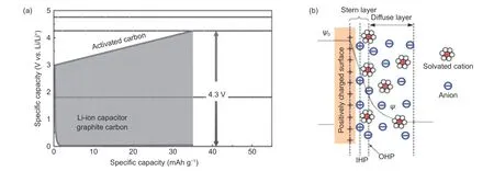
Fig. 1 The schematic diagrams of (a) charging process of LICs[1] (Copyright 2012, Springer New York), and (b) charging mechanism of electric double-layer electrodes [15](Copyright 2009, Royal Society of Chemistry).
According to the electrochemical double layer theory, the charge storage capacity of capacitive energy storage materials is mainly composed of the electronic capacitance (CM) depending on the physical and chemical properties of the material, and the double layer capacitance (CEDL) occuring at the electrode electrolyte interface[8]. Fig. 1b is the currently widely accepted Stern model. In this model, the electrolyte at the electrode interface can be divided into an inner Helmholtz layer and an outer ion diffusion layer, so that electric double layer capacitance can be further subdivided into Helmholtz layer capacitance (CH) and diffusion layer capacitance (Cdiff). The capacitance of the entire electrode interface (Ctotal) has the following relationship with the capacitance of each part[9,10]:

Among them,CM,CHandCdiffare the capacitances of the electrode material, the Helmholtz layer and the diffusion layer of the electrolyte respectively.The electric double layer capacitance (CEDL) is affected by the interface interaction between the electrolyte and the electrode material[11], while the electronic capacitance (CM) mainly depends on the electronic structure of the electrode material[12]. The graphene materials’ electronic capacitance is usually limited by its low electronic density of states (DOS) near the Fermi level, which represents the quantities of states where electrons can occupy, so the electronic capacitance of graphene materials is also called quantum capacitance (CQ), such concept was firstly defined by Luryi[13]. At the interface of the graphene electrode,theCQof the graphene material is much lower than the electric double layer capacitance at the electrode interface[14].CQrestricts the overall performance of LICs using graphene as the positive electrode active material.
In order to improve theCQof graphene materials,the scientific community has proposed a variety of graphene modification ideas, such as doping and functionalizing graphene with elements such as N, B, P,and O to change the electronic structure of graphene and improve DOS near the Fermi level[16,17]. Meanwhile, as the lack of carbon atoms changes the p-electron arrangement of carbon atoms in the graphene lattice, the electronic structure of graphene will also change accordingly[18], such phenomenon leads to the vacancy defect-induced increasing of DOS near the Fermi level[19]. As experimental methods are difficult to accurately control defects, theoretical simulation methods[12,16,20–24]are used increasingly to study the influence of graphene structural characteristics on itsCQ. Sruthi et al.[17]studied the influence of N adsorption and doping at different positions of graphene on theCQ, and discussed the influence of N and oxygen co-doping on theCQof graphene. They found that the presence of oxygen atoms can greatly increase theCQof N-doped graphene. Su et al.[21]studied theCQof different defect structures such as Stone-Wales defect(SW), single vacancy, 3 types of double vacancies (5-8-5, 555-777 and 5555-6-7777, detailed description is given in Fig. 2 below), as well as the pyrrole-N and pyridine-N graphene in the voltage range of LIC’s positive electrode. It is found that the existence of the above-mentioned common defects can significantly improve theCQof single-layer graphene, and the source of capacitance is discussed in detail.
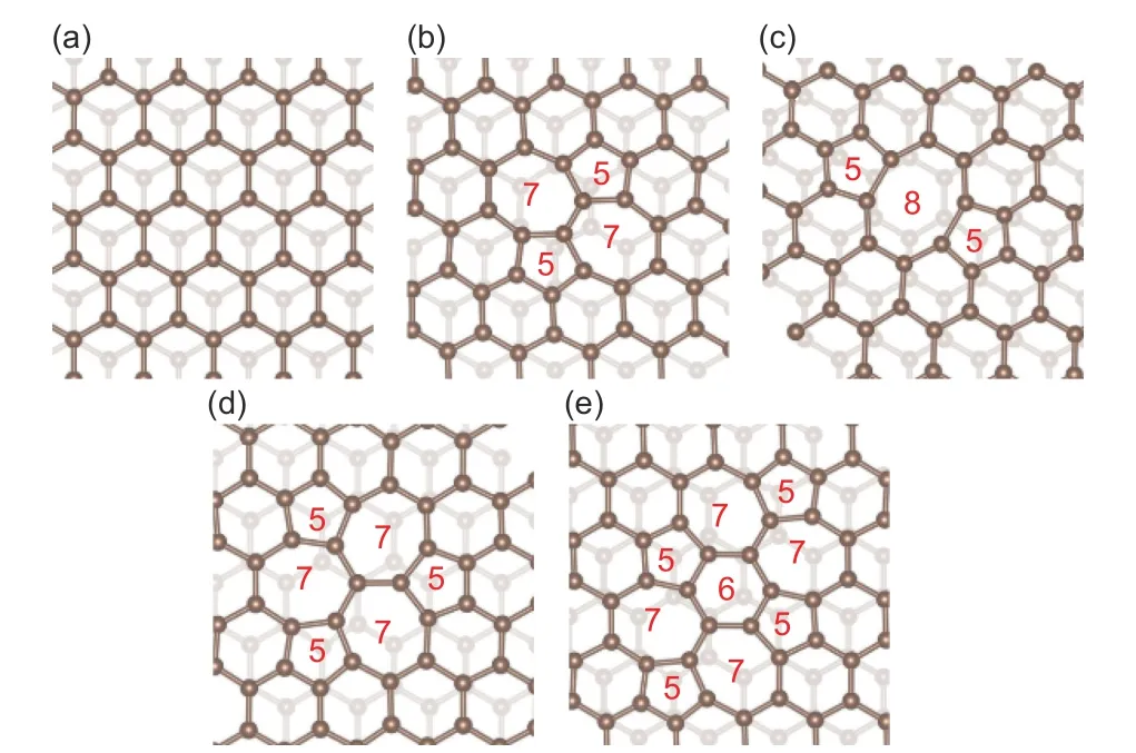
Fig. 2 Configurations of defected bilayer graphene containing point-defects. (a) pristine bilayer graphene, (b) SW type (55-77) defected bilayer graphene, (c) D2_Ⅰ type (the defected carbon rings are arranged as 585 structure) defected bilayer graphene, (d) D2_Ⅱ type (555-777) defected bilayer graphene and (e) D2_Ⅲ type (5555-6-7777)defected bilayer graphene.
In the preparation process of graphene materials,double-layer or even multi-layer stacked graphene is often obtained[25,26]. Moreover, during the use of the energy storage device, with repeated charging and discharging, graphene sheets tend to stack up[25]. The interaction between the stacked graphene sheets changes their electronic structures[27], which in turn affectsCQ.Therefore, when studying theCQperformance of graphene, in order to be closer to the actual situation,theCQof graphene materials in relation to double-layer or multi-layer stacking must be considered in order to be close to the actual situation when theCQof graphene is studied.
Based on the density functional theory (DFT),this paper conducts a computational study on theCQof two-layer stacked graphene, including the pristine graphene with a complete lattice structure and the defective or heteroatoms doped graphene.
Considering the following two factors, only twolayer stacked graphene is calculated in this article.
(1) The principal applied force between the stacked graphene sheets is the Van der Waals force[28]generated by the interaction between the delocalized π-electrons of different sheets. The theoretical interlayer spacing is about 0.355 nm. In the scene of supercapacitors with extremely high charge density, the interacting Debye shielding distance is much smaller than this value[29,30], so the interaction between graphene sheets separated by more than one layer can be ignored almost. It is assumed that when the number of stacked graphene layers continues to increase,the performance change pattern should be similar to that of double layer stacking situation.
(2) When an external electric field is applied,there will be a potential difference between the inner graphene and the surface graphene, which contacts the electrolyte. Under the framework of DFT theory, due to calculation mechanism this potential difference cannot be effectively simulated[31]. Therefore, when the number of stacked layers is large, the reliability of the theoretical calculation results is reduced. Only when the number of stacked graphene layers is no more than two, the theoretical calculation will be close to the actual situation as no potential difference exits between graphene layers.
2 Calculation method
The VASP5.4.1[32]software based on DFT[33]was selected to complete the calculation, the PBE-GGA functional[34]based on generalized gradient approximation (GGA) was used to calculate the exchange correlation energy, the interaction between the valence electron layer and the nucleus and inner electrons was described by the plane wave pseudopotential (PAW)method[35]. The kinetic energy cutoff plane wave basis was set to be 550 eV. The graphene supercell had a 6×6 structure with a lattice constant of 1.479 6 nm,and a vacuum layer with a thickness of 2 nm was set above the graphene sheet. Ion position was optimized by the conjugate gradient algorithm. The lattice constant was fixed. When all the forces were less than 0.1 eV/nm, the system was considered to be fully optimized. The layer spacing of the optimized multi-layer stacked graphene is about 0.315 nm, which varies slightly with the type of defects. The precisions of Kpoint grids were set to be 3×3×1, 7×7×1, and 9×9×1 respectively to sample the Brillouin zone during system optimization, single-point energy calculation, and density of state (DOS) calculation.
Considering that the bias voltage range of a LIC’s positive electrode material during the charging process is about 0–1.0 V[2,36], as the whole work voltage window of LICs is about 2.2–3.8 V (vs Li+/Li)[37], we set the calculation voltage range between 0 and 1.0 V in this paper. At the same time, in order to improve the calculation efficiency, it is assumed that the electronic arrangement of the graphene material would not be affected by the external applied voltage.
The calculation method of graphene surface charge andCQis set as follow:
The surface charge (Q) of graphene is calculated by using the following formula,

In which DOS(E) is the density of state of graphene, f(E) is the Fermi-Dirac distribution function of electrons, andEis the relative energy based on the Fermi level. According to the definition of capacitance, theCQof graphene is calculated as dQ/dφ,

In whichφis the applied voltage on the graphene electrode.
The equation 2-4 illustrate thatCQis the derivative of surface charge with respect to applied voltage,or surface charge is the integral ofCQwith respect to applied voltage.
Excessive Surface Charge Density (σ), or ESCD for short, is the increase in surface charge relative to the initial condition when the applied voltage changes,

3 Results and discussion
3.1 Point defect
We first calculate theCQof the pristine doublelayer graphene and the double-layer graphene with 4 different types of point defects. The basal layer of the model is the pristine single-layer graphene and the surface layer is the defective single-layer graphene.The specific structure are shown in Fig. 2. They are pristine double-layer graphene (Fig. 2a) and 4 different kinds of point-defect double-layer graphene such as SW type (55-77 ring structure, Fig. 2b), D2_Ⅰtype with 585 ring structure (Fig. 2c), D2_Ⅱ type with 555-777 ring structure (Fig. 2d) and D2_Ⅲ type with 5555-6-7777 ring (Fig. 2e).
3.1.1 A comparisonCQof different kinds of stacking graphene
Fig. 3 shows theCQwaveforms (Fig. 3a) and surface charge (Fig. 3b) of all the above-mentioned types of double-layer graphene. It can be seen from Fig. 3a that theCQof the pristine double-layer graphene increases linearly with the increase of voltage, reaching a maximum value of 37.7 μF cm−2at 1.0 V. TheCQwaveform of SW-type defected double-layer graphene is very close to that of pristine double-layer graphene.However, theCQwaveforms of other double-vacancy defected double-layer graphene have significant fluctuations, all showing U-shaped changes. TheCQvalues of D2_Ⅰ, D2_Ⅱ and D2_Ⅲ double-layer graphene decrease with the increase of voltage when the voltage is low. When the voltage reaches 0.17, 0.35 and 0.43 V, theCQwaveforms of the three double-vacancy double-layer graphene achieve the lowest values of 14.5, 19.1 and 19.9 μF cm−2respectively for D2_Ⅰ, D2_Ⅱ and D2_Ⅲ. When the voltage continues to increase, all theCQvalues show an increasing trend. The maximum values appear when the voltage is 1.0 V, which are 49.5, 54.3 and 56.1 μF cm−2, respectively for D2_Ⅰ, D2_Ⅱ and D2_Ⅲ, significantly higher than that (37.7 μF cm−2) of the pristine double-layer graphene under the same voltage.
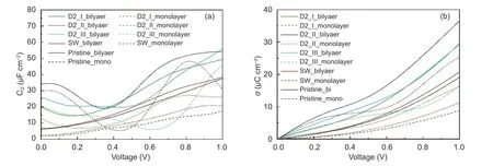
Fig. 3 (a) Specific quantum capacitance (CQ) and (b) excessive surface charge density (ESCD)waveforms for the defected graphene before and after stacking.
Fig. 3b shows the electrical charge on the surface of each topology of the double-layer graphene in the voltage range of 0–1.0 V. It can be seen that the defective double-layer graphene can provide far more free charges in the voltage range of 0–1.0 V than the pristine double-layer graphene. At 1.0 V, the charge provided by the pristine double-layer graphene is only 19.2 μC cm−2. The SW defected double-layer graphene has a slightly higher value. Three types of double-vacancy defected double-layer graphene provide much higher charge. Among them, the D2_Ⅱdefected double-layer graphene has the highest ESCD value of 36.6 μC cm−2at 1.0 V, which is higher than the D2_Ⅰ double-layer graphene (29.4 μC cm−2) and D2_Ⅲ double layer graphene (29.6 μC cm−2).
3.1.2 A comparison ofCQbefore and after stacking
In this article, it is more focused on theCQdifference between the double-layer graphene and singlelayer graphene. It can be seen from Fig. 3a that theCQvalues of double-layer graphene of any topology are higher than that of single-layer graphene, indicating that the graphene has a significantCQincrease after stacking. Affected by this, the surface charge density also increases after stacking. The largest increase in surface charge happens on the D2_I type defected graphene. Compared with the single-layer D2_I type graphene, the double-layer one’s charge at 1.0 V has increased by 13.1 μC cm−2. Even for the smallest increase in SW type defects, an increasing of 9.6 μC cm−2is observed after stacking.
At the same time, the stacking of graphene sheets also eases the fluctuation of theCQvalue waveform.Compared with the single-layer graphene before stacking, the double-layer graphene has a smootherCQwaveform. In particular, the maximumCQvalues of the D2_Ⅱ and D2_Ⅲ-type defected double-layer graphene are 184% and 182% higher than the minimum values, respectively, much less than the gaps of 795% and 659% before stacking. The absolute extreme differences of theCQvalues of the two topologies in the stacking condition are 35.2 and 36.2 μF cm−2, which are also smaller than the extreme difference of 42.9 and 39.8 μF cm−2before stacking.
Stacking also reduces the performance gap among different graphene topologies. At 1.0 V, the D2_Ⅱ double-layer graphene has a 24.5% higher surface charge value than that of D2_Ⅰ double-layer graphene, and the absolute difference is 7.2 μC cm−2.Also at this voltage value, D2_Ⅱ and D2_Ⅰsinglelayer graphene have a surface charge difference of 16.77 μC cm−2, and the former has a twice lager surface charge value than that of the latter.
3.1.3 The effect of stacking on electronic structure
Fig. 4 shows the DOS diagrams of various double-layer and single-layer graphene. It can be seen that regardless of the defect type, the DOS waveform of double-layer graphene is larger than that of singlelayer graphene, and the waveform becomes flat. Since DOS reflects the material’s ability to provide electrons (valence band) or the ability to accommodate electrons (conduction band), the increase in DOS value means the improve of energy storage capacity,and the flattening of the DOS waveform leads to the ease ofCQwaveform. Therefore, after the single-layer graphene is stacked into double-layer graphene, theCQand surface charge increase, and the waveform’s fluctuation amplitude with the voltage change also tends to be flat.
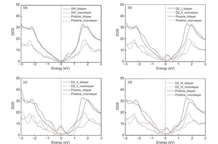
Fig. 4 Comparison of density of states (DOS) between the defected double-layer graphene and the defected single-layer graphene with same defect types.(a) DOS of SW type defected graphene, (b) DOS of D2_Ⅰ type defected graphene, (c) DOS of D2_Ⅱ type defected graphene and(d) DOS of D2_Ⅲ type defected graphene.
At the same time, graphene with similar topological structures get much more similar DOS waveform after stacking. It can be seen from Fig. 4a that the double-layer SW-type defected graphene’s waveform and double-layer pristine graphene’s waveform get more similar than that of the single-layer case.From Fig. 4b, c, and d, it can be seen that in the interval of −1.5–0 eV, the DOS difference between the three double-layer double-vacancy defected graphene is also significantly reduced than that before stacking.Therefore, reflected in the performance ofCQ, the energy storage capacity of SW defected graphene and pristine graphene is still similar after stacking, while the performance difference between the three types of two-vacancy graphene significantly reduces after stacking.
In order to further clarify the electron source that causes the above changes, the charge density in the energy range of −1.5–0 eV on the DOS waveform(hereinafter referred to as the band decomposition charge density, or shortly as BDCD diagram) was analyzed. Fig. 5 shows the BDCD diagrams of different types of graphene materials. It can be seen from Fig. 5 that both the surface and basal layers of the double-layer graphene material provide charges. Two layers of the pristine double-layer graphene provide the same amount of charge (Fig. 5a), but when the surface layer has defects, the amount of charge provided by the defected layer is often much higher than that of the basal layer (Fig. 5b, c, d).
As both of the layers participate in providing charge, the stacked double-layer graphene increases the surface charge. Furthermore, compared with the single-layer defected graphene, the additional pristine substrate layer of the double-layer graphene buffers the difference inCQcaused by the difference in the defected layer structure.
For different defect structures, their effects on the substrate layer are different, resulting in various amounts of charge provided by the substrate layer in the double-layer graphene with different defect structures, which leads to the different stacking causedCQgrowth for different defect graphene materials.

Fig. 5 Diagram of band decomposition charge density (BDCD) of (a) ideal double-layer graphene, (b) SW type defected double-layer graphene,(c) D2_Ⅰtype double layer graphene, (d) D2_Ⅱ type double-layer graphene, (e) D2_Ⅲ type double-layer graphene. In front views the defected layers are at the top, while in side views the defected layers are on the right. (iso=0.006 e Bohr−3).
The existence of the basal layer also strengthens the charge-supply ability of the defected layer. Taking the D2_I graphene as an example, which in this section has the largest increase in energy storage capacity after stacking, from Fig. 5 and Fig. 3b we can find that its energy storage capacity has increased by 80.4%, which obviously exceeds the summation value of isolated monolayer pristine layer and defected layer[21], indicating that the defected layer can provide more charge after stacking.
3.2 Dangling-bond defects
Single-vacancy defects (SV-type defects),pyrrole-N and pyridine-N defects are three basic types of graphene defects containing dangling bonds. Their structural models are shown in Fig. 6.
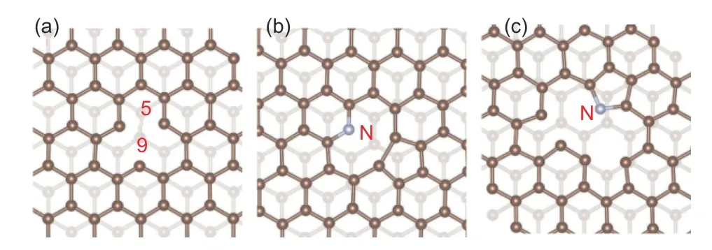
Fig. 6 Configurations of three types of defected double-layer graphene with dangling bonds. (a) SV type(single-vacancy) defected double-layer graphene, (b) pyridinic-N double-layer graphene and(c) pyrrolic-N double-layer graphene.
SV-type defects can be obtained by removing one carbon atom from pristine graphene, which usually causes Jahn-Teller distortion[38]. In this case, two of the three adjacent unsaturated carbon atoms tend to form bonds and the 3rdcarbon atom is sp3hybridized,resulting in a single electron occupying one of the hybridized orbitals.
Pyrrole-N doping and pyridine-N doping can be regarded as defects containing N-doping atoms derived from SV defects. Pyrrole-N doping refers to the substitution of a carbon atom in a five-membered carbon ring with a sp3hybridized N atom[39]. Two of its five valence electrons bind with adjacent carbon atoms, while another two valence electrons occupies a hybridized orbital and merges into the delocalized πelectron system, the remaining one unbonded valence electron occupies a hybridized orbital. Pyridine-type N doping refers to the substitution of sp2hybridized N atom for the dangling carbon atom in the sixmembered ring. Two of the five valence electrons of a N atom form bonds with adjacent carbon atoms, while a third valence electron occupies the pzorbital which is not involved in the hybridization and merges into the delocalized π-electron system, the remaining lone pair valence electrons occupy a hybridized orbital.Since these three kinds of defects all contain an unsaturated dangling bond occupied by a single electron,they are collectively referred to as graphene materials with dangling bond defects.
3.2.1 Comparison ofCQvalues of stacking graphene
As shown in Fig. 7, theCQand surface charge values of the three dangling-bond defected doublelayer graphene are all higher than the pristine doublelayer graphene within the calculated voltage range (0–1.0 V). In the mid-to-high voltage range (0.3–1.0 V),theCQvalues of the two N-doped double-layer graphene types are all significantly higher than the SV-type double-layer graphene and the aforementioned double-layer graphene types.

Fig. 7 Diagram of (a) specific CQ and (b) ESCD of the defected double-layer graphene with dangling bonds.
TheCQwaveform of the SV-type double-layer graphene fluctuates greatly. The peak and bottom values ofCQare obtained at 0.16 and 0.48 V, respectively, which are 34.0 and 22.1 μF cm−2. The maximum value of 46.8 μF cm−2happens at 1.0 V. In the voltage range of 0–0.3 V, theCQvalue of SV-type double-layer graphene is slightly higher than that of N-doped double-layer graphene. There is not much difference between theCQwaveforms of the two Ndoped double-layer graphene types as theCQvalues of both ;are generally increasing with voltage within the calculated voltage range. When the external voltage reaches 1.0 V, the pyridine-N double-layer graphene reaches the maximum value of 75.5 μF cm−2, which is slightly higher than that (72.4 μF cm−2) of the pyrrole-N double-layer graphene.
All these three types of dangling-bond doublelayer graphene have higher charge storage capacity than the pristine double-layer graphene and other aforementioned graphene types as such dangling-bond owners have higherCQvalues in the entire calculation voltage range. When the voltage reaches 1.0 V,the surface charge value of SV-type double-layer graphene reaches 30.84 μC cm−2, while two N-doped double-layer graphene types have higher values, the pyridine-N graphene surface charge is 39.2 μC cm−2,and the pyrrole-N double-layer graphene surface charge is 40.3 μC cm−2. It can be seen that among the double-layer graphene topologies calculated in this work, N-doped ones have the highest charge storage capacity.
3.2.2 Comparison ofCQbefore and after stacking
All the three dangling-bond graphene types get theirCQimprovement after stacking, especially the Ndoped graphene after the voltage exceeds 0.3 V. Such improvement causes a rapid-grow gap between the surface charge value of single-layer N-doped graphene and N-doped double-layer graphene after the voltage exceeds 0.4 V.
In terms of fluctuation trend, unlike the graphene defect structures described in Section 3.1, the fluctuations ofCQwaveforms of the SV-type graphene and pyridine-N defect graphene are not alleviated by stacking.
After stacking, the surface charge value of SVtype graphene gets improved in the entire calculated voltage range, but N-doped graphene types do not exhibit such trends until the voltage exceeds 0.4 V. The energy storage capacity gap between the two N-doped graphene types is reduced after stacking, as the relative difference reduces from 19.6% to 3.0% at 1.0 V.
3.2.3 Effect of stacking on the electronic structure
It can be seen from Fig. 8 that the DOS waveforms of all the three dangling-bond graphene have higher density values after stacking, which brings about improvements of theCQ. In the range of −1.0–0 eV, the DOS waveform of SV-type graphene fluctuates even more sharply after stacking, especially a conspicuous single electron peak, which signifies a fluctuantCQwaveform. The DOS waveform of the pyridine-N graphene has similar variation tendency with that of the SV-type graphene, but the DOS waveform of the pyrrole-N graphene has been significantly alleviated after stacking. Therefore, only theCQof the pyrrole-N graphene has a smaller changing magnitude after stacking.

Fig. 8 Comparison of DOS between double-layer graphene and single-layer graphene with same type of defects.(a) SV-type defect graphene, (b) pyrrolic-N graphene and (c) pyridinic-N graphene.
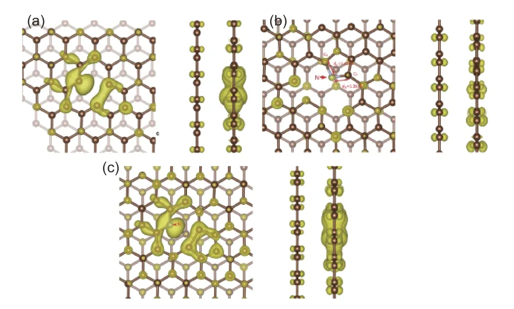
Fig. 9 Diagram of BDCD of (a) SV-type defected double-layer graphene,(b) pyrrolic-N doped double-layer graphene and (c) pyridinic-N doped double-layer graphene. At the left column there are front views of the BDCD plots, while the side views are at the right column. (iso = 0.006 e Bohr−3).
In order to explore the source of energy storage capability, Fig. 9 shows the BDCD diagrams of the three dangling-bond double-layer graphene types in the energy range of −1.0-0 eV. It can be seen from Fig. 9 that typical p-orbital illustrations appear on the SV-type double-layer graphene and the pyridine-N double-layer graphene. In the SV-type defect, the unpaired electron from the dangling carbon atom occupies the p-orbital, while in the pyridine-N defect, it is the lone pair electrons from the doped N atom that settle in the p-orbital. In contrast, the charge density diagram of pyrrole-N double-layer graphene has no sign of unbonded electrons. Furthermore, the bond length between the doped N atom and two adjacent carbon atoms is different as more electric charges are distributed on the carbon atoms that form longer bonds with the N atom. It is speculated that a single electron may have entered the anti-bonding orbital of the chemical bond between the N atom and such carbon atom.
Since the defected layer, especially the defect itself provides most of the charge during the charge storage process, theCQwaveforms of SV-type graphene and pyridine-N graphene cannot be alleviated by the additional basal layer which comes from stacking. However, since the basal layer contributes more charge during the energy storage process, theCQwaveform of the pyrrole-N graphene has a smoothly fluctuating shape.
In addition, based on the surface charge value at 1.0 V, the charge storage capacities of SV-type graphene, pyridine-N graphene and pyrrole-N graphene increase by 50.4%, 73.1% and 49.1% respectively after stacking. The improvement in storage capacity obviously exceeds the ability of single-layer pristine graphene, or basal layer discussed about, indicating that the existence of basal layer enhances the charge storage capability of the three types of dangling-bond graphene.
4 Conclusions
TheCQcharacteristics of a variety of double-layer graphene with different atomic structures are theoretically studied by DFT. According to the theoretical calculation, the following conclusions are drawn:
(1) By stacking, regardless of the surface defects and element composition of graphene, both the value and waveform ofCQof graphene are changed. For graphene with no unpaired electrons, the waveform is alleviated after stacking. TheCQwaveforms of the SV and N-doped graphene are relatively insensitive to stacking.
(2) Due to the improvement ofCQ, the surface charge of graphene materials is increased after stacking, especially for the N-doped graphene. In addition,stacking reduces the energy storage performance difference between graphene materials with similar structures.
(3) The main reason for the improvements in the energy storage performance of graphene materials by stacking is due to the charge of the substrate layer, the charge provided by the defected layer is simultaneously increased by interlayer interaction. As a result,theCQvalues of most graphene topologies have been significantly improved after stacking. In addition, the uniform distribution of charges on the base layer graphene moderately alleviates the fluctuation of theCQwaveform.
Acknowledgements
This work was supported by The DNL Cooperation Fund, CAS (DNL201915), Research and Development Project of Key Core and Common Technology of Shanxi Province (20201102018) and National Science Foundation for Excellent Young Scholars of china (21922815).
- 新型炭材料的其它文章
- Preparation of a porous carbon from Enteromorpha prolifera with excellent electrochemical properties
- High-surface-area porous carbons produced by the mild KOH activation of a chitosan hydrochar and their CO2 capture
- 基于碳化钽涂层改性碳基材料的研究进展
- Preparation of a N-P co-doped waste cotton fabric-based activated carbon for supercapacitor electrodes
- Coating a Na3V2(PO4)3 cathode material with carbon to improve its sodium storage
- Two-dimensional layer materials for highly efficient molecular sensing based on surface-enhanced Raman scattering

