
Phototransistor Based on Single TaON Nanobelt and Its Photoresponse from Ultraviolet to Near-infrared
2019-10-10 02:10TAOYouRongCHENJinQiangWUXingCai
无机材料学报 2019年9期
TAO You-Rong, CHEN Jin-Qiang, WU Xing-Cai
Phototransistor Based on Single TaON Nanobelt and Its Photoresponse from Ultraviolet to Near-infrared
TAO You-Rong, CHEN Jin-Qiang, WU Xing-Cai
(Key Laboratory of Mesoscopic Chemistry of MOE, State Key Laboratory of Coordination Chemistry, School of Chemistry and Chemical Engineering, Nanjing University, Nanjing 210023, China)
TaON nanobelts (NBs) were controllably synthesized by Ta2O5NBs template-conversion method. The typical NBs have cross-sections of 40 nm×200 nm–400 nm×5600 nm, and lengths up to about 0.5 cm. A field effect transistor (FET) based on single TaON NB was fabricated on SiO2/Si substrate. The electronic mobility and on-off ratio of the nanobelts are 9.53×10⁻⁴cm2/(V·s) and 3.4, respectively. The FET shows good photoresponses from 254 nm to 850 nm. Under irradiation of 405 nm light (42 mW/cm2), the responsivity is 249 mA/W at a bias of 5.0 V, and the photoswitch current ratio is 11. Therefore, the phototransistor shows a good photodetectivity, and TaON NBs may become good candidates for fabricating optoelectronic devices. Additionally, Ta2O5@TaON composite NBs were also synthesized, and a FET based on the single NB was fabricated. Under irradiation of the same light, its photoresponse is weaker than TaON NB, but it is still a good optoelectronic material.
TaON nanobelt; template synthesis; field effect transistor; photodetector
One-dimensional (1D) nanostructures of semiconductors have extensively been applied as functional building blocks for electronic and optoelectronic devices such as field-effect-transistors (FETs)[1], chemical sensors[2], electronic field emitters[3-4], photodetectors[5-7], solar cells[8], and supercapacitors[9], because the reduced dimension brings about new physical-chemical properties, and 1D nanostructures are suitable for nanofabrication. Research shows that the high photoconductive gains of the low dimensional semiconductor photodetectors depend on both their high surface-area-to-volume ratios (SVRs) and the reduced dimension of the effective conductive channel, because the high SVRs can increase the number of surface trap states and prolong photocarrier lifetime, whereas the reduced dimensionality can confine the active area of the charge carrier, and shorten the transit time[10]. Photodetector from the ultraviolet (UV) to the infrared (IR) is critical for industrial and scientific applications such as images sensing, communications, environmental monitoring, remote control, day-and- night-time surveillance, and chemical/biological sensing[11]. Although a few photodetectors based on nanostructures of metal oxides[12-13], metal chalcogenides[14], transition metal dichalcogenides (TMDs)[15-16], and transition metal trichalcogenides (TMTs)[17-18], are reported, it is still a challenge to develop low-cost, nontoxicity, high-detectivity and broadband response photodetector.
TaON is a semiconductor with a band gap of 2.4 eV[19]. Its powders were once proposed as a nontoxic yellow pigment[20]. Recently, they have been used as visible- light-driven photocatalyts to split water[21]and oxidize methanol[22]. TaON powders could be prepared by calcination of Ta2O5powders in the flowing NH3, for example, Ta2O5could be totally converted to TaON in the flowing NH3of 10 mL/min at 800 ℃ for 10 h, while totally converted to Ta3N5in a flowing NH3of 1000 mL/min at 800 ℃ for 10 h[23]. We once synthesized Ta3N5nanobelts (NBs) by direct aminolysis of TaS3NBs at high temperature, and discovered its good photosensitive properties from 250 nm to 630 nm[24]. In order to develop new photosensitive materials, here a Ta2O5NB template conversion method was employed to synthesize TaON NBs, and reaction time was reduced to 3 h. Phototransistor based on single TaON NB shows good photoresponse from ultraviolet (UV) to near infrared (NIR), and have higher photoswitch current ratio (PCR) than Ta3N5NB photodetector[24].
1 Experiment
1.1 Preparation of TaON nanobelts
Firstly, TaS3NBs were prepared by chemical vapor transport method[25-26]. In typical process, 825 mg of tantalum (Ta) foil (99.9%, 0.2 mm×5 mm×45 mm), 146 mg of sulfur (S) powders (99.99%), and 15 mg of iodine (I2) powders (99.8%) were sealed in a quartz ampoule in vacuum (0.6 cm×12 cm,10–2Pa). The Ta foils were adjusted at the center of the ampoule and then the ampoule was placed at the center of a conventional horizontal furnace (4 cm×32 cm) with a temperature gradient of10 ℃/cm from center to end. Then the furnace was heated to 550 ℃ at a rate of 10 ℃/min, kept at 550 ℃ for 8 h, and cooled naturally to room temperature. TaS3NBs on the Ta foils were extracted from the ampoule.
Secondly, TaS3NBs were directly oxidized into Ta2O5NBs at 650 ℃ for 2 h in air.
Finally, the Ta2O5NBs were transferred into quartz coat, and placed in the center of the quartz tube of the horizontal furnace, then converted into green-yellow TaON NBs at 850 ℃ for 3 h in the flowing atmosphere of Ar (20 mL/min)/NH3(80 mL/min) with a rising temperature rate of 10 ℃/min.
1.2 Characterization
The products were characterized by X-ray diffractometer (XRD) under monochromatized Cu Kα-radiation (Shimadzu XRD-6000), LEO-1530VP scanning electron microscope (SEM), JEOL-JEM-2010 high-resolution electron microscope (HRTEM) using imaging and selected area electron diffraction (SAED) with an energy dispersive X-ray spectrometer (EDX). The UV-Vis absorbance spectra of the products were recorded by UV- 3600 spectrophotometer (Shimadzu UV-3600).
1.3 Device fabrication and measurements
To fabricate field-effect-transistor (FET) of single NB, the TaON NBs were suspended in ethanol by brief sonication and then deposited on Si substrate with 300 nm thick thermal oxide layer serving as gate oxide. The standard photolithography technique followed by Ti/Au (10 nm/100 nm) metal evaporation and lift off were used to define the source and drain electrodes electrically contacting the NBs. The current-voltage (-) and current- time (-) characteristics of the photodetector were measured by SM-4 probe system and Keithley 236 source meter. The spectroscopic response ranging from 350 nm to 900 nm was measured using a 300 W Xe lamp (HSXUV300), and a multi-grating monochromator (71SW151) with ordered sorting filters. Small Lasers and ultraviolet lights were also used. Optical powers were measured with FZ-A, UV-340B, and UV-B radiometers. All measurements were carried out in air at room temperature.
2 Results and discussion

A FET based on a single TaON NB is depicted in Fig. 3(a). AFM image of the FET is represented in Fig. 3(b), and the height profile of the corresponding NB is shown in inset. The nanobelt between two electrodes is 1.42 μm in width, 4.34 μm in length, and 92 nm in thickness. Fig. 3(c) displays-characteristics at gate voltage (g) from –20 V to 20 V. It shows that the conductance of the NB increases monotonically as gate voltage increases, indicating that TaON NB is an n-type semiconductor. The transfer characteristic of the FET at bias of 1 V is shown in Fig. 3(d). Theds-gplot shows a threshold voltage (th) of about 16 V, and a linear-region transconductancem(dds/dg) of 3.59×10⁻¹²A/V. An on-off ratio of 3.4 is measured. The electronic mobility () can be calculated from the following equations:=m/(0ds), whereandare width and length of channel, respectively, and0is the gate capacitance. Assuming a parallel plate capacitor model,0=0r/, whereis the dielectric constant (r=3.9 for SiO2,0= 8.854×10⁻¹²F/m), andis the thickness (300 nm) of the gate oxide layer[28]. From above equation, the mobility is calculated to be 9.53×10⁻⁴cm2/(V·s).

Fig. 1 (a) XRD pattern, (b) low-magnification SEM image (inset: light photograph), and (c) high-magnification SEM image of TaON nanobelts; (d) TEM image of a single TaON nanobelt withinset in the middle showing corresponding HRTEM image, and inset on the upper right corner showing FFT pattern of HRTEM image
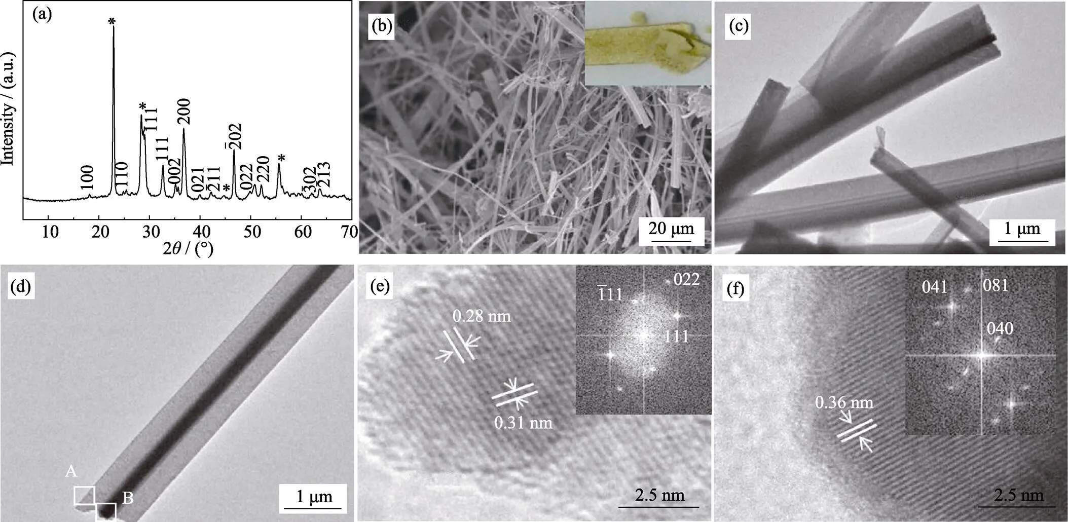
Fig. 2 (a) XRD pattern (a peak with star representing Ta2O5, and the rest peaks representing TaON), (b) low-magnification SEM image (inset: light photograph), and (c) TEM image of Ta2O5@TaON composite nanobelts; (d) TEM image of a single Ta2O5@TaON nanobelt; (e, f) HRTEM images of square A and B in (d), respectively with insets showing FFT patterns of corresponding HRTEM images

Fig. 3 (a) Scheme of FET based on a single TaON nanobelt; (b) Overlooked AFM image of the FET with inset showing size profile of the nanobelt; (c) Ids-Vds plots at different Vg; (d) Ids-Vg plot at Vds= 1 V
Fig. 4(a) shows a TaON NB FET which the channel is 0.71 μm in width and 8.5 μm in length, respectively. Fig. 4(b) is the-curves of the TaON NB FET exposed to different wavelength light and under dark conditions, which exhibits good photoresponse from 254 nm to 850 nm. Based on the data, responsivities to 254, 365, 405, 532, 650, 780 and 850 nm at a bias of 5 V are 199, 237, 347, 53, 45, 28, and 47 mA/W, respectively. The responsivity (R) and external quantum efficiency () are related to the number of electron-hole pairs excited by one absorbed photon, so highRandcorrespond to the high sensitivity.R= Δ/(PS), and=hcR/(), where Δis the difference between the illumination current and the dark current,is the light power intensity,is the irradiated area, andis the light wavelength[24]. Fig. 4(c) shows the responsivities of the FET from 350 nm to 900 nm, so the cut-off wavelength is about 900 nm. As wavelength increases, the change trend is similar to UV-Vis absorption spectrum of the NBs (inset in Fig. 4(c)). Fig. 4(d) shows the-curve of the FET under illumination of 405 nm light with a power of 42 mW/cm2at a bias of 5 V with a photoswitch period of 1 s. Based on data of Fig. 4(d),405 nm= 249 mA/W,=7.2×105%, and PCR is 11. Here the responsivity is lower than that of Fig. 4(b), which can be attributed to the fact that current recovery needs more time under photoswitch. Fig. 4(e) displays the local-magnitude curve from 3.2 s to 5.6 s in Fig. 4(d), showing that the rise and recovery time of the photoswitch current are less than 0.2 s, limited by instrument. Fig. 4(f) is the-curve of the FET under illumination of 405 nm light with the same power and bias voltage with a photoswitch period of 50 s, showing good stability of the photodetector.
Fig. 5(a) reveals micrograph of the FET based on a single Ta2O5@TaON NB. The nanobelt between two electrodes is 1.4 μm wide and 7.1 μm long, respectively. Fig. 5(b) exhibts the responsivities of the FET to different wavelength light, showing the cut-off wavelength of about 900 nm. The change trend is similar to UV-Vis absorption spectrum of the NBs (inset). Here the responsivity at 350 nm approaches that at 400 nm, which may be attributed to the fact that photogenerating electrons of Ta2O5join in photocurrents because Ta2O5has only strong absorption at UV region. Fig. 5(c) shows the-curves of the FET exposed to different-wavelength light. It also shows good photosensitive properties from 254 nm to 850nm. Fig. 5(d) shows the-curve of the FET under illumination of 405 nm light (42 mW/cm2) at a bias of 5 V with a photoswitch period of 50 s. Here405 nm,, andare 3.9 mA/W, 1.1×10⁴%, and 2, respectively, and rise and decay time of the photoswitch currents is less than 0.2 s, limited by instrument. For comparison, a few results are included in Table 1. Based on Table 1, single TaON NB photodetector has higher responsivity than single-layer MoS2and single GaS-nanobelt. Compared with Ta3N5-NB photodetector, the TaON NB photodetector has lower responsivity, but higher, so it is still good photodetector. Under the same illumination conditions, the single TaON NB photodetector higherand responsivity than the single Ta2O5@ TaON NB photodetector, so the former is superior to the latter. It may be attributed that Ta2O5@TaON NB contains less TaON than TaON NB, and bandgap of Ta2O5(3.9 eV) is greater than that of TaON (2.2 eV), so that photogenerating electrons of the composite NB reduce under illumination of the same light, so the photoresponse dwindles.

Fig. 4 (a) Photograph of a single TaON nanobelt FET, (b) I-V characteristics of the FET illuminated and unilluminated with different wavelength light, (c) responsivities of the FET to different wavelengths with inset showing UV-Vis absorption spectrum of TaON NBs, (d, f) transient photoresponses of the FET illuminated by 405 nm (42 mW/cm2) light pulse chopped with a photoswitch period of 1 and 50 s at bias of 5 V and (e) local magnification of (d) from 3.2 s to 5.6 s
3 Conclusion
In the work, a Ta2O5NB template-synthesis route to TaON NB has been provided, which confirms that template- conversion is an efficient way to prepare nanowires (or NBs). Ta2O5@TaON composite NBs can be also prepared by controlling conditions. The phototransistors based on both individual nanobelts show good responses from 254 nm to 850 nm. Compared with Ta2O5@TaON NB, TaON NB shows higher responsivity and, but both may still become good candidates for optoelectronic devices, and can even be used in photocatalysis field.

Fig. 5 (a) Photography of FET based on a single Ta2O5@TaON nanobelt, (b) photoresponsivities of the FET to different wavelengths with inset showing UV-Vis absorption spectrum of Ta2O5@TaON NBs, (c) I-V characteristics of the FET unilluminated illuminated with different wavelength light, and (d) transient responses of the FET illuminated with a 405 nm (42 mW/cm2) light pulse chopped with a photoswitch period of 50 s at a bias voltage of 5 V

Table 1 Comparision of TaON NB photodetector with others reported
[1] GLUSCHKE J G, SEIDL J, BURKE A M,. Achieving short high-quality gate-all-around structures for horizontal nanowire fieldeffect transistors., 2019, 30(6): 064001–1–7.
[2] LIANG J R, ZHAO Y R, ZHU K L,. Synthesis and room temperature NO2gas sensitivity of vanadium dioxide nanowire structures by chemical vapor deposition., 2019, 669: 537–543.
[3] ZHANG Y L, WU X C, TAO Y R,. Fabrication and field-emission performance of zirconium disulfide nanobelt arrays., 2008(23): 2683–2685.
[4] WU X C, HONG J M, TAO Y R,. Controlled growth and field-emission properties of NbSe2micro/nanostructured films., 2010, 10(10): 6465–6472.
[5] TAO Y R, WU X C, XIONG W W. Flexible visible-light photodetectors with broad photoresponse based on ZrS3nanobelt films., 2014, 10(23): 4905–4911.
[6] TAO Y R, WU J J, WU X C. Enhanced ultraviolet-visible light responses of phototransistors based on single and a few ZrS3nanobelts., 2015, 7(34): 14292–14298.
[7] TIAN W, ZHANG C, ZHAI T Y,. Flexible ultraviolet photodetectors with broad photoresponse based on branched ZnS-ZnO heterostructure nanofilms.,2014, 26(19): 3088–3093.
[8] VETTORI M, PIAZZA V, CATTONI A,. Growth optimization and characterization of regular arrays of GaAs/AlGaAs core/shell nanowires for tandem solar cells on silicon., 2019, 30(8): 08400–1–15.
[9] GU S S, LOU Z, MA X D,. CuCo2O4nanowires grown on a Ni wire for high-performance flexible fiber supercapacitors., 2015, 2(7): 1042–1047.
[10] PENG L, HU L F, FANG X S. Low-dimensional nanostructure ultraviolet photodetectors., 2013, 25(37): 5321–5328.
[11] GONG X, TONG M H, XIA Y J,. High-detectivity polymer photodetectors with spectral response from 300 nm to 1450 nm., 2009, 325(5948): 1665–1667.
[12] BORUAH B D, MUKHERJEE A, MISRA A. Sandwiched assembly of ZnO nanowires between graphene layers for a self-powered and fast responsive ultraviolet photodetector., 2016, 27(9): 095206–1–11.
[13] ZHAO Y M, FENG S L, JIANG H T,. Catalyst-free growth of a Zn2GeO4nanowire network for high-performance transfer-free solar-blind deep UV detection.,2019, 107: 1–4.
[14] GERTMAN R, HARUSH A, VISOLY-FISHER I. Nanostructured photocathodes for infrared photodetectors and photovoltaics., 2015, 119(4): 1683–1689.
[15] WU J J, TAO Y R, WU Y,. Ultrathin SnS2nanosheets of ultrasonic synthesis and their photoresponses from ultraviolet to near-infrared., 2016, 231: 211– 217.
[16] HAFEEZ M, GAN L, LI H Q,. Large-area bilayer ReS2film/multilayer ReS2flakes synthesized by chemical vapor deposition for high performance photodetectors., 2016, 26(25): 4551–4560.
[17] XIONG W W, CHEN J Q, WU X C,. Visible light detectors based on individual ZrSe3and HfSe3nanobelts., 2015, 3(9): 1929–1934.
[18] TAO Y R, CHENJ Q, WU J J,Flexible ultraviolet-visible photodetector based on HfS3nanobelt film., 2016, 658: 6–11.
[19] CHUN W J, ISHIKAWA A, FUJISAWA H,. Conduction and valence band positions of Ta2O5, TaON, and Ta3N5by UPS and electrochemical methods., 2003, 107(8): 1798–1803.
[20] BERTAUX S, REYNDERS P, HEINTZ J M,. New (oxy) nitride pearlescent pigments., 2005, 121 (1/2): 137–144.
[21] CHEN S S, QI Y, HISATOMI T,. Efficient visible-light-driven Z-scheme overall water splitting using a MgTa2O6-xN/TaON heterostructure photocatalyst for H2evolution., 2015, 54 (29): 8498–8501.
[22] ITO S, THAMPI K P, COMTE P,. Highly active meso- microporous TaON photocatalyst driven by visible light., 2005(2): 268–270.
[23] NAKAMURA R, TANAKA T, NAKATO Y. Oxygen photoevolution on a tantalum oxynitride photocatalyst under visible-light irradiation: how does water photooxidation proceed on a metal- oxynitride surface?, 2005, 109(18): 8920–8927.
[24] WU X C, TAO Y R, LI L,. Centimeter-long Ta3N5nanobelts: synthesis, electrical transport, and photoconductive properties., 2013, 24 (17): 175701.
[25] WU X C, TAO Y R, GAO Q X,. Superconducting TaS2-xIhierarchical nanostructures., 2009(28): 4290–4292.
[26] WU X C, TAO Y R, GAO Q X. Fabrication of TaS2nanobelt arrays and their enhanced field-emission., 2009(40): 6008–6010.
[27] XIE X, KWOK S Y, LU Z Z,. Visible-NIR photodetectors based on CdTe nanoribbons., 2012, 4(9): 2914–2919.
[28] YIN Z Y, LI H, LI H,. Single-layer MoS2phototransistors., 2012, 6(1): 74–80.
[29] HU P A, WANG L F, YOON M,. Highly responsive ultrathin GaS nanosheet photodetectors on rigid and flexible substrates., 2013, 13(4): 1649–1654.
基于单根TaON纳米带的光晶体管与紫外到近红外响应
陶友荣, 陈晋强, 吴兴才
(南京大学 化学化工学院, 教育部介观材料重点实验室, 配位化学国家重点实验室, 南京 210023)
用Ta2O5纳米带模板转化法控制合成TaON纳米带, 典型的纳米带长约0.5 cm, 横截面积40 nm×200 nm~ 400 nm×5600 nm。在SiO2/Si基片上加工出TaON单根纳米带的场效应晶体管; 该晶体管的电子迁移率和开关比分别为9.53×10⁻⁴cm2/(V·s)和3.4, 在254~850 nm范围内显示良好的光响应。在405 nm (42 mW/cm2)的光照下, 外加5.0 V的偏压时, 光响应为249 mA/W, 光开关比为11。因此, 该器件具有良好的光探测性, TaON纳米带可作为光电子器件的候选材料。另外, 实验还控制合成出Ta2O5@TaON纳米带, 并加工成单根纳米带的场效应晶体管, 虽然相同光照条件下的光响应弱于TaON 纳米带, 但仍算是一种好的光电材料。
TaON纳米带; 模板合成; 场效应晶体管; 光探测器
TQ174
A
2018-12-14;
2019-03-12
National Natural Science Foundation of China (21673108); Open Foundations of State Key Laboratory of Coordination Chemistry (SKLCC1622)
TAO You-Rong (1964–), female, associate professor. E-mail: yrtao@nju.edu.cn
WU Xing-Cai, Professor. E-mail: wuxingca@nju.edu.cn
1000-324X(2019)09-1004-07
10.15541/jim20180584
猜你喜欢
实用手外科杂志(2022年2期)2022-08-31
中外文摘(2022年12期)2022-08-02
科学导报(2022年17期)2022-04-02
大自然探索(2021年7期)2021-09-26
表面技术(2021年3期)2021-04-07
建材发展导向(2019年10期)2019-08-24
电子制作(2019年11期)2019-07-04
筑路机械与施工机械化(2016年3期)2016-03-22
居业(2015年16期)2016-02-24
科学中国人(2015年8期)2015-06-09
