
铱衬底上异质外延单晶金刚石: 过程与机理
2019-10-10 02:03王杨朱嘉琦扈忠波代兵
无机材料学报 2019年9期
王杨, 朱嘉琦, 扈忠波, 代兵
铱衬底上异质外延单晶金刚石: 过程与机理
王杨, 朱嘉琦, 扈忠波, 代兵
(哈尔滨工业大学 复合材料与结构研究所, 哈尔滨 150080)
金刚石因其独特的物理化学性质, 在探测器、光电子器件等领域得到了广泛的应用, 单晶金刚石更是因为具有大幅度提高这些器件功能的潜力而引起了众多学者的关注。目前在铱(Ir)衬底上异质外延生长的单晶金刚石具有最大尺寸和较为优异的生长质量。本文介绍了可用于外延金刚石的不同结构的衬底以及金刚石在铱(Ir)衬底上的形核和生长过程, 重点阐述了金刚石偏压辅助形核(BEN)和外延横向生长(ELO)的机理, 以及衬底图形化形核生长技术, 指出了目前研究存在的不足, 并对金刚石异质外延理论和实验研究方向进行了展望。
单晶金刚石; 异质外延; 偏压辅助形核; 外延横向生长; 综述
金刚石是自然界中硬度最大[1]、固体材料中导热率最高[2]的材料, 且具有从远红外到近紫外宽波段光学透明[3]和负电子亲和势[4]等独特性质, 被广泛应用于探测器[5-6]、散热器件[7]、光学器件[8]和光电子器件[9]等领域。单晶金刚石由于具有无晶界、缺陷少、性能优等优点, 得到研究者越来越多的关注。
单晶金刚石的制备方法主要有高温高压(High Pressure High Temperature, HPHT)法和化学气相沉积(Chemical Vapor Deposition, CVD)法[10]。HPHT法需要极高的温度(1230~1600 ℃)和压力(5.1~ 5.6 GPa)[11-12]条件, 制备的单晶金刚石杂质含量较多, 且尺寸难以超过1 cm3。
CVD法包括同质外延和异质外延两种。侧向生长是在籽晶<100>晶面的不同侧面反复外延的一种同质外延方法, Mokuno等[13]利用侧向生长法获得了尺寸为12.6 mm×13.3 mm×3.7 mm的单晶金刚石, 但籽晶尺寸和反复生长次数都会限制金刚石的尺寸。另一种同质外延方法是马赛克拼接法, 利用经Yamada等[14-15]改进后的马赛克拼接法可得到尺寸为40 mm×60 mm的单晶金刚石晶片, 但接缝处的生长缺陷会延伸至晶片内部, 影响晶片质量。
目前在铱衬底上异质外延单晶金刚石是解决上述问题的一种可行方法。因此, 一些研究机构和团队开始进行大尺寸单晶金刚石异质外延制备的研究, 奥格斯堡大学的Schreck等[16]在Ir(100)衬底上利用异质外延法制备了直径达92 mm的单晶金刚石。国内也有高校对异质外延法制备大尺寸单晶金刚石开展了初步实验研究[17-20]。异质外延单晶金刚石的技术关键是衬底的选择与金刚石的形核和生长, 本文将综述这两个方面近年来的研究进展, 并指出异质外延金刚石理论和实验中亟待解决的问题。
1 基于铱(Ir)的不同衬底结构
一般来说, 选择合适的金刚石异质外延衬底需考虑衬底的物理性质、化学性质、晶格失配度、尺寸等因素[21]。为寻找最佳的金刚石异质外延衬底, 研究者们研究了Si[22-24]、c-BN[25-26]、Pt[27]、Ni[28-29]、SiC[30-31]等不同材料, 图1为在一些常用衬底上异质外延生长的金刚石的表面形貌。从图中可见在Ir衬底上生长的金刚石具有与单晶类似的平滑形貌, 而生长在其他衬底上的几乎均为单一取向或近单一取向的多晶金刚石。
Ir是目前唯一可实现高质量、大尺寸金刚石薄膜异质外延的衬底材料。第一性原理计算结果表明,碳原子在Ir中的溶出能(Dissolution energy)对其浓度变化十分敏感, 当碳原子浓度增加时, Ir衬底中的碳原子迅速失稳析出, 该溶解–析出过程导致衬底表面形貌快速变化, 有利于金刚石晶粒在Ir衬底表面的平移和旋转从而快速达到一致取向[35]。
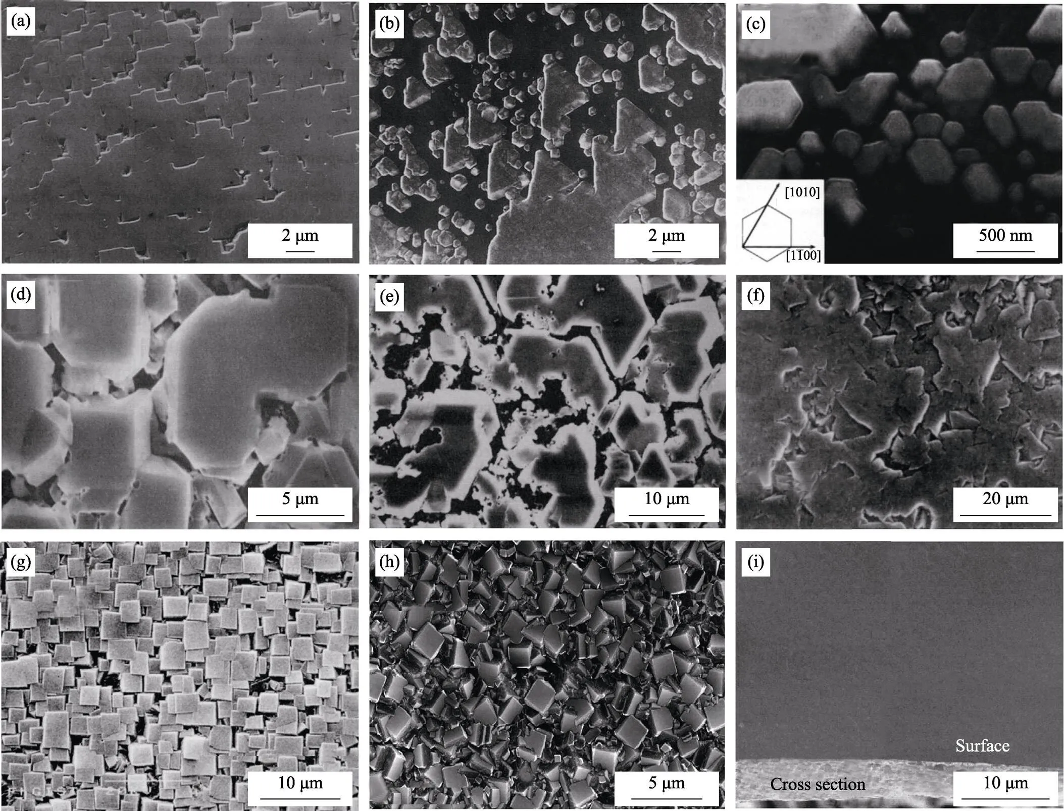
图1 不同衬底上异质外延生长的金刚石的表面形貌[32-34]
(a) c-BN(001); (b) c-BN(111); (c) Al2O3(0001); (d) Ni(001); (e) Ni(111); (f) Pt(111); (g) Si(001); (h) 4H-SiC(001); (i) Ir(001)
除极少数专利使用纯Ir金属片作为衬底[36]外, 其他报道中均使用Ir薄膜作为金刚石异质外延衬底。Ir薄膜可以利用磁控溅射[37-38]、脉冲激光沉积[39]、电子束蒸镀[40]、分子束外延[41]等方法制备, 一般外延于MgO[42]、SrTiO3[43]和蓝宝石[44]等氧化物单晶上。由于金刚石和这些金属氧化物之间热膨胀系数的差异, 在达到金刚石薄膜外延温度(950 ℃以上)时, 单晶氧化物衬底上沉积的金刚石薄膜中的热应力σ达到–4~–8 GPa, 金刚石薄膜在生长至微米级厚度之后极易脱落[45]。
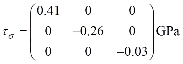
而由于金刚石与硅的热膨胀系数较接近, 在Si上沉积的金刚石薄膜内部的热应力相对较低(–0.68 GPa), 在较高沉积温度下甚至更低[46], 例如在Si(100)/YSZ(100)/Ir(100)衬底上生长的金刚石薄膜, 其内应力33接近于0, 应力矩阵如式(1)所示:
但硅与铱元素之间的化学反应使得Ir薄膜不能直接沉积于Si衬底, 因此需要在Si衬底和Ir层之间沉积缓冲层。根据最底层衬底及缓冲层材料的不同, 可以形成不同的多层膜结构, 仅列出在Ir(100)晶面外延金刚石的生长质量, 如表1所示。
其中, 生长质量利用由X射线摇摆曲线半高宽得到的面内倾斜角(tilt, Δ)和面外扭转角(twist, Δrot)进行表征。由表1可知, 在Ir(100)衬底上外延生长的金刚石薄膜均能达到极高的质量。但以Si(100)作为衬底最底层时, 外延生长的单晶金刚石薄膜厚度可以达到较高的水平。与较小尺寸的氧化物单晶片相比, 尺寸大且热膨胀系数与金刚石相近的Si单晶片为制备大尺寸自支撑金刚石晶片提供了技术可能。外延金刚石薄膜与各层衬底的取向关系为diamond(100) [100]||Ir(100)[100]||MO(100)[100] ||Si(100)[100][54]。
2 金刚石的形核过程
2.1 偏压增强形核法与初级核的形成
衬底在微波等离子体化学气相沉积(MPCVD)系统中共需经历H2清洗、甲烷稳定化处理、形核和金刚石薄膜生长四个过程, 各步骤的参数如表2所示。对于形核过程, 一般来说, 形核密度越大, 金刚石的生长质量越高, 最常用的增强形核方法为偏压增强形核(Bias Enhanced Nucleation, BEN)法。在微波化学气相沉积系统中, 既可以将负偏压直接施加到衬底上, 也可以使衬底接地, 在等离子体球上施加正电压[55-56]。
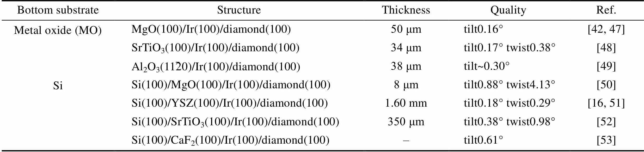
表1 基于Ir(100)衬底的不同膜系结构上金刚石的外延质量
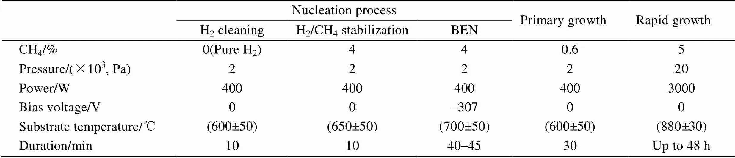
表2 金刚石在Ir上形核及生长过程的实验参数[59]
等离子体球在施加偏压时会发生形变, 产生特殊的偏压辉光区, 如图2所示, 该过程增大了等离子球与衬底的接触面积, 同时加速了离子运动, 有利于金刚石的大面积形核, 同时可以提高形核密度和均匀性[58]。
BEN过程开始后, 铱衬底表面先形成非晶碳层(图3(b1)), 偏压为离子提供的能量使得含碳离子进入Ir衬底的亚表面形成过饱和固溶体, 碳再从亚表面析出形成初级金刚石晶核(图3(b2))[65]。由于Ir和金刚石具有相近的二次电子发射系数, 金刚石在Ir上形核实际上是刻蚀金刚石大颗粒的过程[66]。由于该过程抑制了金刚石颗粒的生长, 可以持续进行较长时间, 有利于金刚石大面积均匀形核[67], 形核密度可以达到3×1011cm–2[16]。但金刚石在Ir上形核的最佳偏压和甲烷体积分数的取值范围较窄[68],在该范围之外取值则会造成形核密度急剧下降[56]。
图2 施加偏压时等离子体球的形状变化[57]
(a) Photograph; (b) Schematic
2.2 次级核的形成与衬底的表面形貌
初级核形成后, 会重整、规范其周围碳原子排列结构形成排列规则的金刚石晶核, 从而不断扩大形核区, 形成次级核(图3(b3))。可以在扫描电子显微镜照片中观测到该明亮区域[69], 这是形核过程的特征形貌, 也是之后金刚石晶核生长的区域[70]。原位观测BEN过程及生长过程后的衬底, 可见外延的晶粒几乎全部位于之前形成的明亮岛状区域内,这些区域外部几乎没有晶粒, 如图4所示。可以利用这种现象, 在衬底上预先设置“形核区”, 从而达到选区外延效果, 这也属于一种衬底图形化的方法[71]。
停止施加偏压并开始金刚石的生长过程5~10 s后, 在生长过程最初阶段腔体内甲烷浓度升高的情况下, 之前因离子撞击稳定沉积在衬底表面的无定型碳薄膜被快速刻蚀[45], 如图3(b4)所示。
3 金刚石的生长过程
3.1 缓慢生长阶段
金刚石生长过程可以分为缓慢生长和快速生长两个阶段, 生长过程参数见表2所示。缓慢生长过程即新金刚石晶核与形核阶段金刚石晶核的连接与晶体尺寸增加过程。
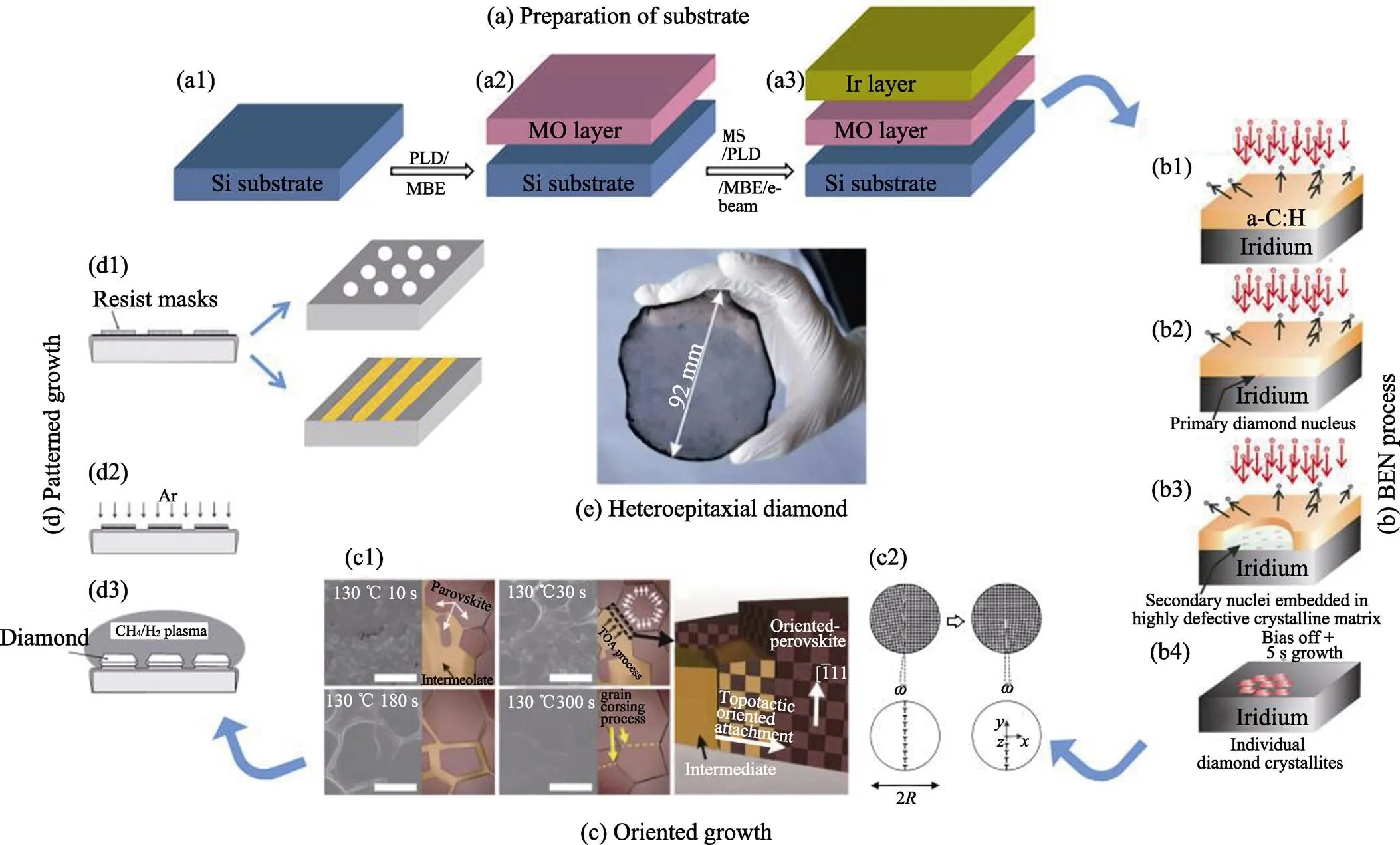
图3 单晶金刚石在铱(Ir)衬底上异质外延的过程示意图[16, 60-64]
(a) Preparation of substrate; (b) Bias Enhanced Nucleation (BEN) process; (c) Oriented growth; (d) Patterned growth; (e) Heteroepitaxial diamond
MS: Megnetron Sputtering; PLD: Pulsed Laser Deposition; MBE: Molecular Beam Epitaxy
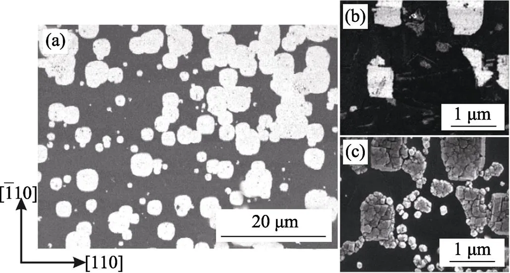
图4 利用二次电子探测器观测到的SEM照片[72]
(a) BEN过程后铱衬底表面形貌; (b) BEN过程后铱衬底局部表面形貌; (c)生长过程后同一位置形貌
Fig. 4 SEM images[72]of the iridium surface after BEN treatment (a), local spots after BEN (b) and after a subsequent growth step (c)
比较常见的晶体材料的生长机制有奥斯特瓦尔德熟化(Ostwald Ripening, OR)[73]、定向附着生长(Oriented Attachment, OA)[74]和柯肯达尔效应(Kirkendall Effect, KE)[75]等。定向附着生长是团簇沿着特定的晶向聚集并最终形成单晶或孪晶的过程, 具有非随机性[76]。由于金刚石在Ir衬底上较高的形核密度, 金刚石生长的最初阶段更倾向于OA生长机制, 可以认为定向附着生长即为金刚石缓慢生长阶段的微观机理。
Li等[77]首次利用透射电子显微镜观测到液体中晶粒的定向附着生长过程, 如图5所示。Dong等[69]在外延薄膜中观测到薄膜和过渡层晶粒的拓扑衍生定向附着生长现象, 如图3(c1)所示。Dideikin等[78]以爆轰法制备的纳米金刚石为原料, 在高温高压条件下, 纳米金刚石颗粒相接触并发生倾斜、旋转, 每两个颗粒的相同晶面通过悬挂键相连接, 最终形成1.5 μm的单晶金刚石颗粒, 从而验证了固体颗粒之间的定向附着生长机制。但是对于金刚石在形核生长过程中的原位过程还缺少相应的研究仪器和研究方法, 以至于金刚石的生长过程难以通过直观的方法进行观测。
定向附着生长过程中, 晶界湮没形成金刚石单晶是小角度晶界形成的楔形向错所导致的。图3(c2)为立方晶中的小角晶界及部分形成楔形向错的结构示意图, 楔形向错对应于一个不完整的倾斜晶界[70]。可以推出晶粒尺寸和晶界转变为楔形向错的临界角crit之间的关系为[32]:
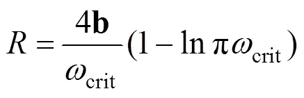
其中,为柱状晶粒半径, b为柏氏矢量。
还有一些研究者采用晶体相场法模拟异质外延形核生长过程[79]和晶界湮没过程[80], 将晶界看作若干刃型位错, 并在生长或施加应力、温度场过程中不断正负抵消, 最终晶界被完全移出晶体表面而消失, 从而形成单晶。
3.2 衬底图形化生长方法
在晶体外延生长领域, 定向附着生长又可以称为外延横向生长(Epitaxial Lateral Overgrowth, ELO)[81]。根据ELO原理所延伸出的图形化生长方法(Patterned Nucleation and Growth, PNG), 可以有效地减少Ir和金刚石界面处贯穿位错的产生[82]。该过程的主要步骤为: 在已经完成形核步骤的金刚石薄膜表面覆盖点状或条纹状Au[83]、Ni[84]等材料的模板层(图3(d1)), 利用等离子体刻蚀该表面(图3(d2)), 或在金刚石形核后利用光刻将表面刻蚀成以Ir为生长模板、金刚石核为边框的栅格网络[85], 再继续之后的生长过程[71](图3(d3))。
另外, 可用HPHT法生长的金刚石作为衬底, Ir作为模板层[72, 86], 或者可在金刚石薄膜生长到一定厚度时, 将其刻蚀成纳米针, 并在这些纳米针表面完成金刚石薄膜的后生长[87-88], 甚至在该过程中直接使用HPHT单晶金刚石作为衬底, 进行保护后刻蚀成纳米针[84], 这些方法均可视作以Ir衬底上金刚石异质外延为基础的特殊的同质外延方法。
利用衬底图形化方法, 可有效地提高金刚石薄膜的生长质量, 其面内倾斜角的值可降低至0.064°, 面外扭转角可低至0.043°[85], 与马赛克法同质外延生长的金刚石在非边缘接缝处测得的数值在同一数量级(面内倾斜角Δ= 0.012°)[89]。
3.3 快速生长阶段
金刚石薄膜在快速生长过程开始后, 随着厚度的增加, 其表面形貌、结构和镶嵌度都会有一定的改善, 贯穿位错逐渐消失[90], 为异质外延生长大尺寸单晶金刚石提供了可能性。图6(a~c)为金刚石薄膜形貌的连续变化过程, 薄膜从由小颗粒组成最终生长成有缺陷的单晶。当厚度为8 μm时, 直径为 1 mm的单晶区域被由位错组成的封闭的晶界网络包围, 厚度增加到34 μm时, 晶界网络已经分解成由位错团簇组成的较短位错带[48]。
图6(d)利用(400)和(311)晶面X射线摇摆曲线半高宽表征面内倾斜角(Δ)和面外扭转角(Δrot), 从而说明在Ir衬底上外延金刚石薄膜的镶嵌度随金刚石薄膜厚度的变化。最初金刚石薄膜具有较大的面内倾斜角和面外扭转角, 在随后的薄膜生长过程中, 倾斜角和扭转角均随薄膜厚度增加显著降低, 该变化说明金刚石外延质量得到了明显提高[91]。也可利用Raman光谱检测缺陷结构的变化, 对于1 μm的薄膜, Raman峰半高宽>10 cm–1, 而对于厚度约为950 μm的薄膜, 半高宽值下降至1.86 cm–1, 接近于完美的金刚石单晶, 同时缺陷密度从>1010cm–2下降至<108cm–2[92]。这些研究均表明随着金刚石薄膜厚度的增加, 其生长质量有所提高, 这是异质外延的一项显著优点。这就使得异质外延生长的单晶金刚石可以在保证其良好质量的同时, 达到较高的厚度水平, 为之后在各种器件中的复杂应用提供了合适的材料基础[91]。
由于最终生长的金刚石晶片中仅存在线缺陷, 而不再含有多晶材料中典型的连续晶界网络, 所以在Ir衬底上异质外延的金刚石为单晶金刚石。这主要是由于形核和生长阶段中以下的几个影响因素所导致的: 首先, 形核过程所加偏压对于金刚石大颗粒的刻蚀作用导致金刚石在Ir衬底上大面积、高密度均匀形核[66-67], 且由于Ir-C之间独特的溶解–析出相互作用过程[35], 同时C原子在偏压辅助形核过程中倾向溶解于Ir衬底亚表面形成过饱和固溶体[65], 均会导致C原子在亚表面和近表面区域有极高的运动速率, 为初级核的平移和旋转提供驱动力, 从而易于形成与衬底相同的取向; 在次级核形成的过程中, C原子的快速移动也会导致规则排列的sp3结构的晶核快速规整排列不够整齐的结构, 最终形成统一的sp3结构[16]; 另外晶粒表面由于附着大量的非饱和碳氢悬挂键, 由前述过程所形成的次级核相互接触形成的薄膜的镶嵌度<1°, 晶粒之间易于通过定向附着生长的原理进行连接[78], 以向错代替晶界, 最终形成完整的单晶金刚石。
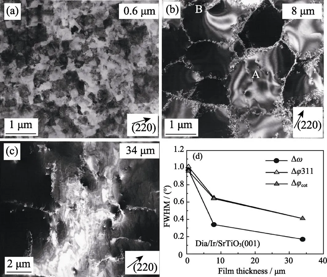
图6 Ir/SrTiO3(100)上外延的不同厚度金刚石薄膜[48]
(a-c) TEM images; (d) Reduction in mosaic spreaded with increasing thickness
4 总结与展望
Ir衬底上异质外延金刚石的研究已经持续了30多年, 得到的单晶金刚石薄膜质量在不断提高, 尺寸也在不断增大。本文对于在Ir衬底上异质外延金刚石的过程进行了描述和机理分析, 目前已有研究对单晶金刚石异质外延衬底进行了合理的设计和制备, 同时对单晶金刚石在Ir衬底上的形核、生长过程的各个阶段进行了理论上的解释, 并提出了一些提高金刚石外延尺寸和质量的方法。作为唯一一种技术上可实现的能够制备大尺寸、高质量单晶金刚石, 从而满足其在各个领域应用的方法, 金刚石的异质外延得到了科学界的广泛关注。但其在以下几个研究方向上仍然存在一些值得深入研究的问题:
1) Ir衬底上金刚石异质外延过程的原位实验研究仍有待深入。目前对于金刚石异质外延过程的实验研究方法依然是以在一定生长时间后暂停实验、取出试件并进行观测为主, 难以对整个过程进行连续、完整的描述。现有的原位透射电镜和原位扫描电镜等实验仪器难以在金刚石生长条件下使用, 需要研究新的实验和观测方法。
2) 金刚石异质外延生长过程中的n型掺杂。金刚石的n型掺杂一直是一项困难的工作, 但异质外延单晶金刚石尺寸大、表面光滑、缺陷密度低, 为其在电子器件中的应用提供了可能性, 基于异质外延金刚石薄膜的n型掺杂是一项亟待研究的课题。
3) 金刚石异质外延理论和全对称材料的制备。目前, 关于在Ir衬底上的金刚石异质外延研究主要集中在实验层面, 理论研究上仍有较大的发展空间。比起晶格常数匹配度更佳的Ni、Cu等材料, Ir在金刚石异质外延领域的出色表现质疑了研究者之前认为晶格常数匹配度是异质外延的重要影响因素的假设。同时, 由于已经实现在金刚石衬底上异质外延Ir薄膜, 即已经实现了金刚石、Ir的相互外延, 为制备全对称材料提供了理论支持, 这对于异质外延理论的发展具有重大意义。
为了使异质外延金刚石能够在相关领域展开应用, 充分利用金刚石的优异性质, 必须进行大规模量产。目前, 异质外延金刚石仅限于在实验室中制备的样品, 但想要应用其优良性能并制作成器件, 尚需对其制备工艺和技术进行进一步优化和研究。
[1] ZOU L, ZHOU M. Experimental investigation and numerical simulation on interfacial carbon diffusion of diamond tool and ferrous metals., 2016, 31(2): 307–314.
[2] ZHANG C, WANG R, CAI Z,. Low-temperature densification of diamond/Cu composite prepared from dual-layer coated diamond particles., 2015, 26(1): 185–190.
[3] NAZARI M, HANCOCK B L, ANDERSON J,. Optical characterization and thermal properties of CVD diamond films for integration with power electronics., 2017, 136(10): 12–17.
[4] ZHU D, BANDY J A, LI S,. Amino-terminated diamond surfaces: photoelectron emission and photocatalytic properties., 2016, 650(8): 295–301.
[5] SHEN H J, WANG L J, HUANG J,. Research for (100)-oriented diamond film radiation detector., 2009, 24(6): 1254–1258.
[6] WILLIAMS T, MARTENS A, CASSOU K,. Novel applications and future perspectives of a fast diamond gamma ray detector., 2017, 845(5): 199–202.
[7] ZHANG R, ZHAO W S, YIN W Y,. Impacts of diamond heat spreader on the thermo-mechanical characteristics of high-power AlGaN/GaN HEMTs., 2015, 52(2): 25–31.
[8] DING M Q, LI L, DU Y,. Development of an extremely thin-diamond window for terahertz traveling wave tubes., 2017, 79(10): 173–178.
[9] WANG J J, HE Z Z, YU C,. Comparison of field-effect transistors on polycrystalline and single-crystal diamonds., 2016, 70(11): 114–117.
[10] KASU M. Diamond epitaxy: basics and applications., 2016, 62(2): 317–328.
[11] KUPRIYANOV I N, KHOKHRYAKOV A F, BORZDOV Y M,. HPHT growth and characterization of diamond from a copper- carbon system., 2016, 69(10): 198–206.
[12] XIAO H Y, LI S S, QIN Y K,. Studies on synthesis of boron- doped Gem-diamond single crystals under high temperature and high presure., 2014, 63(19): 198101.
[13] MOKUNO Y, CHAYAHARA A, YAMADA H,. Improving purity and size of single-crystal diamond plates produced by high-rate CVD growth and lift-off process using ion implantation., 2009, 18(10): 1258–1261.
[14] YAMADA H, CHAYAHARA A, MOKUNO Y,. Effects of crystallographic orientation on the homoepitaxial overgrowth on tiled single crystal diamond clones., 2015, 57(8): 17–21.
[15] YAMADA H, CHAYAHARA A, MOKUNO Y,. Uniform growth and repeatable fabrication of inch-sized wafers of a single- crystal diamond., 2013, 33(3): 27–31.
[16] SCHRECK M, GSELL S, BRESCIA R,. Ion bombardment induced buried lateral growth: the key mechanism for the synthesis of single crystal diamond wafers., 2017, 7: 44462–1–3.
[17] 朱金凤. 微波CVD法制备高质量金刚石颗粒. 武汉: 武汉工程大学硕士学位论文, 2013.
[18] 张景文, 陈旭东, 王进军, 等. 一种基于异质外延生长单晶金刚石的方法. 中国, C30B25/18, CN201710633557. 2017.07.28.
[19] LI Y F, SHE J M, SU J J,. Heteroepitaxial nucleation of diamond on Ir(100)/MgO(100) substrate by bias enhanced microwave plasma chemical vapor deposition method., 2015, 44(4): 896–901.
[20] 王杨, 代兵, 朱嘉琦, 等. 一种异质外延生长大尺寸单晶金刚石的衬底及其制备方法. 中国, C30B29/04, CN201410794743.0. 2015.04.08.
[21] SARTORI A, FISCHER M, GSELL S,.boron doping during heteroepitaxial growth of diamond on Ir/YSZ/Si., 2012, 209(9): 1643–1650.
[22] LIAO K J, WANG W L, FENG B. Effect of nucleation rate on heteroepitaxial diamond growth on Si (100)electron-emission- enhanced nucleation by hot filament chemical vapor deposition., 1998, 167(1): 117–123.
[23] ZHAO S, HUANG J, ZHOU X,. Highly dispersible diamond nanoparticles for pretreatment of diamond films on Si substrate., 2018, 434(3): 260–264.
[24] LIU C, WANG J H, WENG J. Preparation of the high-quality highly (100) oriented diamond films with controllable growth., 2015, 64(2): 028101.
[25] GAO F, JIA X P, MA H A,. Hetero-epitaxial diamond single crystal growth on surface of cBN single crystals at high pressure and high temperature., 2008, 25(6): 2273–2276.
[26] WANG C X, GAO C X, ZHANG T C. Preparation of p-n junction diode by B-doped diamond film grown on Si-doped c-BN., 2002,19(10):1513–1515.
[27] HAYASHI Y, MATSUSHITA Y, SOGA T,. The formation of a (111) texture of the diamond film on Pt/TiO2/SiO/Si substrate by microwave plasma chemical vapor deposition., 2002, 11(3–6): 499–503.
[28] SITAR Z, LIU W, YANG P C,. Heteroepitaxial nucleation of diamond on nickel., 1998,7(2):276–282.
[29] ITO S, NAGAI M, MATSUMOTO T,. Self-separation of freestanding diamond films using graphite interlayers precipitated from C-dissolved Ni substrates., 2017,470(14): 104–107.
[30] HE X C, SHEN H S, ZHANG Z M,. Growth of CVD heteroepitaxial diamond on silicon (001) and its electronic properties., 2000,9(9):1626–1631.
[31] CHANG L, LIN T S, CHEN J L,. Transmission electron microscopy study of diamond nucleation on 6HSiC single crystal with possibility of epitaxy., 1993, 62(26): 3444–3446.
[32] SCHRECK M. CVD Diamond for Electronic Devices and Sensors. Chichester: Wiley, 2009: 125–161.
[33] MOORE E, JARRELL J, CAO L. Heteroepitaxial diamond growth on 4H-SiC using microwave plasma chemical vapor deposition., 2017, 3(9): e00404.
[34] SCHRECK M, SCHURY A, HÖRMANN F,. Mosaicity reduction during growth of heteroepitaxial diamond films on iridium buffer layers: experimental results and numerical simulations., 2002, 91(2): 676–685.
[35] VERSTRAETE M J, CHARLIER J C. Why is iridium the best substrate for single crystal diamond growth?, 2005, 86(191): 191917.
[36] 野口仁. 金刚石膜的制造方法. 日本, C30B25/10, CN201510627462.0. 2015.12.23.
[37] MARTOVITSKY V P, EVLASHIN S A, SUETIN N V,. Heteroepitaxial Ir layers on diamond., 2011, 44(21): 21540–1–6.
[38] MEYER F, OESER S, GRAFF A,. Effect of substrate bias on the growth behavior of iridium on A-plane sapphire using radio frequency sputtering at low temperatures., 2018, 650(3): 65–70.
[39] FAN L, JACOBS C B, ROULEAU C M,. Stabilizing Ir(001) epitaxy on yttria-stabilized zirconia using a thin Ir seed layer grown by pulsed laser deposition., 2017, 17(1): 89–94.
[40] GSELL S, FISCHER M, BAUER T,. Yttria-stabilized zirconia films of different composition as buffer layers for the deposition of epitaxial diamond/Ir layers on Si(001)., 2006, 15(4): 479–485.
[41] ARNAULT J C, SCHULL G, MERMOUX M,. BEN-HFCVD effects on diamond nucleation on iridium: a Raman imaging study., 2005, 202(11): 2073–2078.
[42] TSUBOTA T, OHTA M, KUSAKABE K,. Heteroepitaxial growth of diamond on an iridium(100) substrate using microwave plasma-assisted chemical vapor deposition., 2000, 9(7): 1380–1387.
[43] LEE K H, SAADA S, ARNAULT J,. Epitaxy of iridium on SrTiO3/Si(001): a promising scalable substrate for diamond heteroepitaxy., 2016,66(6):67–76.
[44] CHEN Y C, CHANG L. Chemical vapor deposition of diamond on an adamantane-coated sapphire substrate., 2014, 4(36): 18945–18950.
[45] GSELL S, BAUER T, GOLDFUß J,. A route to diamond wafers by epitaxial deposition on siliconiridium/yttria-stabilized zirconia buffer layers., 2004, 84(22): 4541–4543.
[46] GALLHEBER B C, FISCHER M, KLEIN O,. Formation of huge in-plane anisotropy of intrinsic stress by off-axis growth of diamond., 2016, 109(14): 14190–1–7.
[47] ICHIKAWA K, KODAMA H, SUZUKI K,. Dislocation in heteroepitaxial diamond visualized by hydrogen plasma etching., 2016, 600(2): 142–145.
[48] SCHRECK M, HÖRMANN F, ROLL H,. Diamond nucleation on iridium buffer layers and subsequent textured growth: a route for the realization of single-crystal diamond films., 2001, 78(2): 192–194.
[49] SAMOTO A, ITO S, HOTTA A,. Investigation of heterostructure between diamond and iridium on sapphire., 2008, 2(17): 1039–1044.
[50] GSELL S, SCHRECK M, BRESCIA R,. Iridium on biaxially textured oxide templates: a concept to grow single crystals on arbitrary substrates., 2008, 47(12): 8925–8927.
[51] STEHL C, SCHRECK M, FISCHER M,. Thermal diffusivity of heteroepitaxial diamond films: experimental setup and measurements., 2010, 2(19): 787–791.
[52] BAUER T, GSELL S, SCHRECK M,. Growth of epitaxial diamond on siliconiridium/SrTiO3buffer layers., 2005, 14(3–7): 314–317.
[53] LEE C H, QI J, LEE S T,. Epitaxial diamond on a Si/CaF2/Ir substrate., 2003, 12(8): 1335–1339.
[54] BRESCIA R, SCHRECK M, GSELL S,. Transmission electron microscopy study of the very early stages of diamond growth on iridium., 2008, 17(7): 1045–1050.
[55] GSELL S, SCHRECK M, BENSTETTER G,. Combined AFM-SEM study of the diamond nucleation layer on Ir(001)., 2007, 16(4): 665–670.
[56] REGMI M, MORE K, ERES G. A narrow biasing window for high density diamond nucleation on Ir/YSZ/Si(100) using microwave plasma chemical vapor deposition., 2012, 23(3): 28–33.
[57] WHITFIELD M D, JACKMANA R B, FOORD J S. Spatially resolved optical emission spectroscopy of the secondary glow observed during biasing of a microwave plasma., 2000, 56(1): 15–23.
[58] KÁTAI S Z, KOVÁTS A, MAROS I,. Ion energy distributions and their evolution during bias-enhanced nucleation of chemical vapor deposition of diamond., 2000, 9(3): 317–321.
[59] BENSALAH H, STENGER I, SAKR G,. Mosaicity, dislocations and strain in heteroepitaxial diamond grown on iridium., 2016, 66(6): 188–195.
[60] DONG H K, PARK J, ZHEN L,. 300% enhancement of carriermobility in uniaxial-oriented perovskite films formed by topotactic- oriented attachment., 2017, 29(23): 1606831.
[61] MICHLER J, KAENEL Y V, STIEGLER J,. Complementary application of electron microscopy and micro-Raman spectroscopy for microstructure, stress, and bonding defect investigation of heteroepitaxial chemical vapor deposited diamond films., 1998, 83(187): 187–197.
[62] ANDO A, KAMANO T, SUZUKI K,. Epitaxial lateral overgrowth of diamonds on iridium by patterned nucleation and growth method., 2012, 51(9): 090101.
[63] WANG Y F, CHANG X H, LIU Z C,. Lateral overgrowth of diamond film on stripes patterned Ir/HPHT-diamond substrate., 2018, 489(5): 51–56.
[64] YOSHIKAWA T, KODAMA H, KONO S,. Wafer bowing control of free-standing heteroepitaxial diamond (100) films grown on Ir(100) substratespatterned nucleation growth., 2015, 594(11): 120–128.
[65] CHAVANNE A, ARNAULT J C, BARJON J,. Bias-enhanced nucleation of diamond on iridium: a comprehensive study of the first stages by sequential surface analysis., 2011, 605(5): 564–569.
[66] HÖRMANN F, SCHRECK M, STRITZKER B. First stages of diamond nucleation on iridium buffer layers., 2001, 10(9): 1617–1621.
[67] CHAVANNE A, BARJONB J, VILQUIN B. Surface investigations on different nucleation pathways for diamond heteroepitaxial growth on iridium., 2012, 22(2): 52–58.
[68] CHAVANNE A, ARNAULT J C, BARJON J,. Effect of bias voltage on diamond nucleation on iridium during BEN., 2010, 1292(1): 137–140.
[69] SCHRECK M, GSELL S, BRESCIA R,. Diamond nucleation on iridium: local variations of structure and density within the BEN layer., 2009, 18(2): 107–112.
[70] VAISSIEREA N, SAADAA S, BOUTTEMY M,. Heteroepitaxial diamond on iridium: new insights on domain formation., 2013, 36(6): 16–25.
[71] AREND C, APPEL P, BECKER J N,. Site selective growth of heteroepitaxial diamond nanoislands containing single SiV centers., 2016, 108(6): 127–159.
[72] SCHRECK M, BAUER T, GSELL S,. Domain formation in diamond nucleation on iridium., 2003, 12(3): 262–267.
[73] TCHOLAKOVA S, MUSTAN F, PAGUREVA N,. Role of surface properties for the kinetics of bubble Ostwald ripening in saponin-stabilized foams., 2017, 534(12): 16–25.
[74] HAZARIKA S, MOHANTA D. Oriented attachment (OA) mediated characteristic growth of Gd2O3nanorods from nanoparticle seeds., 2016, 34(2): 158–164.
[75] CHEN X C, IM S H, KIM J,. Synthesis of barium-strontium titanate hollow tubes using Kirkendall effect., 2018, 483(2): 102–109.
[76] FICHTHORN K A. Atomic-scale aspects of oriented attachment., 2015, 121(1): 10–15.
[77] LI D S, NIELSEN M H, LEE J R I,. Direction-specific interactions control crystal growth by oriented attachment., 2012, 336(6084): 1014–1018.
[78] DIDEIKIN A T, EIDELMAN E D, KIDALOV S V,. Oriented- attachment growth of diamond single crystal from detonation nanodiamonds., 2017, 75(5): 85–90.
[79] PODMANICZKY F, TÓTH G I, TEGZE G,. Phase-field crystal modeling of heteroepitaxy and exotic modes of crystal nucleation., 2017, 457(1): 24–31.
[80] BOBYLEV S V, GUTKIN M Y, OVID'KO I A. Decay of low-angle tilt boundaries in deformed nanocrystalline materials., 2004, 37(2): 269–272.
[81] KIM D, JEONG W S, KO H,. Pretreatment by selective ion-implantation for epitaxial lateral overgrowth of GaN on patterned sapphire substrate., 2017, 641(11): 2–7.
[82] ICHIKAWA K, KODAMA H, SUZUKI K,. Effect of stripe orientation on dislocation propagation in epitaxial lateral overgrowth diamond on Ir., 2017, 72(2): 114–118.
[83] TANG Y H, GOLDING B. Stress engineering of high-quality single crystal diamond by heteroepitaxial lateral overgrowth., 2016, 108(5): 052101.
[84] AIDA H, KIM S W, IKEJIRI K,. Microneedle growth method as an innovative approach for growing freestanding single crystal diamond substrate: detailed study on the growth scheme of continuous diamond layers on diamond microneedles., 2017, 75(5): 34–38.
[85] ICHIKAWA K, KURONE K, KODAMA H,. High crystalline quality heteroepitaxial diamond using grid-patterned nucleation and growth on Ir., 2019, 94: 92–100.
[86] BAUER T, SCHRECK M, STRITZKER B. Epitaxial lateral overgrowth (ELO) of homoepitaxial., 2007, 16(4): 711–717.
[87] AIDA H, IKEJIRI K, KIM S W,. Overgrowth of diamond layers on diamond microneedles: new concept for freestanding diamond substrate by heteroepitaxy., 2016, 66(6): 77–82.
[88] AIDA H, KIM S W, IKEJIRI K,. Fabrication of freestanding heteroepitaxial diamond substratemicropatterns and microneedles., 2016, 9(3): 035504.
[89] SHU G Y, DAI B, RALCHENKO V G,. Epitaxial growth of mosaic diamond: mapping of stress and defects in crystal junction with a confocal Raman spectroscopy., 2017, 463(4): 19–26.
[90] KLEIN O, MAYR M, FISCHER M,. Propagation and annihilation of threading dislocations during off-axis growth of heteroepitaxial diamond films., 2016, 65(5): 53–58.
[91] SCHRECK M, HÖRMANN F, ROLL H,. Heteroepitaxial diamond films on silicon substrates and on iridium layers: analogies and differences in nucleation and growth., 2001, 11(3): 189–205.
[92] STEHL C, FISCHER M, GSELL S,. Efficiency of dislocation density reduction during heteroepitaxial growth of diamond for detector applications., 2013, 103(15): 151905.
Heteroepitaxial Growth of Single Crystal Diamond Films on Iridium: Procedure and Mechanism
WANG Yang, ZHU Jia-Qi, HU Zhong-Bo, DAI Bing
(Center for Composite Materials and Structures, Harbin Institute of Technology, Harbin 150080, China)
Due to its unique physical and chemical property, diamond is widely used in many fields such as detectors and optoelectronic devices. Many scholars’ attention is drew into single crystal diamond because of its potential to significantly increase the functionality of these devices. Presently, single crystal diamonds grown heteroepitaxially on iridium (Ir) substrates reach the largest size and an excellent growth quality. In this paper, substrates with different structures for nucleation and growth processes of epitaxial diamond are introduced. The mechanisms of diamond nucleation by Bias Enhanced Nucleation (BEN) method and growth undergoing an Epitaxial Lateral Overgrowth (ELO) process are described, including technique of Patterned Nucleation and Growth(PNG). Limitations of current study are pointed out, and the future development of heteroepitaxial theory and experiment are also forecasted in this paper.
single crystal diamond; heteroepitaxial growth; bias enhanced nucleation; epitaxial lateral overgrowth; review
O782
A
1000-324X(2019)09-0909-09
10.15541/jim20180587
2018-12-17;
2019-02-12
国家自然科学基金(51702066); 国家杰出青年科学基金(51625201); 国家重点研发计划 (2016YFE0201600); 国家自然科学基金联合基金重点项目(U1809210)
National Natural Science Foundation of China (51702066); National Science Fund for Distinguished Young Scholars (51625201); National Key Research and Development Program of China (2016YFE0201600); Key Project of National Natural Science Foundation of China (U1809210)
王杨(1991–), 女, 博士研究生. E-mail: ravimassa@163.com
朱嘉琦, 教授. E-mail: zhujq@hit.edu.cn
猜你喜欢
云南化工(2022年10期)2022-11-05
物理学报(2022年15期)2022-08-12
天津大学学报(自然科学与工程技术版)(2022年10期)2022-07-04
人工晶体学报(2022年3期)2022-04-14
海峡科技与产业(2021年6期)2021-12-21
人工晶体学报(2021年10期)2021-11-26
粉末冶金技术(2021年3期)2021-07-28
表面技术(2021年3期)2021-04-07
西安工业大学学报(2020年1期)2020-03-07
筑路机械与施工机械化(2016年3期)2016-03-22
