A Modular DC/DC Photovoltic Generation System for HVDC Grid Connection
Guoen Cao*, Kai Sun, Siyue Jiang, Shilei Lu, and Yibo Wang
(1. Institute of Electrical Engineering, Chinese Academy of Sciences, Beijing 100190, China;2. State Key Laboratory of Power Systems, Tsinghua University, Beijing 100084, China)
Abstract: A modular DC/DC conversion system with distributed MPPT and centralized step-up converter for photovoltaic energy integrated into HVDC grids is proposed in this paper. The conversion system consists of two power stages, with MPPT converter as the first stage and a step-up converter as the second stage. Both stages are modular structures. For the distributed MPPT stage, interleaved boost topology is utilized to effectively reduce the input and output ripples without adding extra components. For the centralized step-up stage, narrow-switching-frequency-variation LLC topology is employed, with the modules being configured as input-parallel-output-series structure. Full-range soft-switching property is achieved in the LLC stage to minimize switching losses. Theoretical analysis is carried out for the system voltage gain and design principles. Simulation and experimental results of a 3kW prototype system are presented to verify the theoretical analysis of the proposed system.
Keywords: Photovoltaic generation, DC-DC converter, HVDC grid connection, cascaded configuration.
1 Introduction
Recently, large-scale centralized photovoltaic(PV)stations have gained significant growth worldwide as one of the most promising types of PV energy utilizations to satisfy the growing urban and industrial demand[1]. In a large-scale centralized high voltage AC(HVAC) grid-connected PV system, PV power is generally converted and allocated into medium-voltage AC grid by several power electronic inverter in parallel and by one or more low frequency step-up transformers.The PV HVAC grid-connected system has advantages of low cost and high power efficiency, and has been widely utilized worldwide[2].
In general, a single-stage conversion scheme, which reduces system cost, power losses, and system bulk, is widely adopted in the large-scale PV system by the major PV manufacturers[3]. However, the single conversion stage presents a reduced overall efficiency due by partial shading. Another typical scheme known as two conversion stage, has the advantage of higher efficiency in the case of partial shading by performing distributed maximum power point tracking(MPPT) algorithm[4].However, this scheme is commonly used in small and medium scale PV system because of high system cost and power quality disturbance. On the other hand,HVAC-connected PV system is confronted with many challenges to the reliability and stability of the main grid,such as reactive power compensation, long-distance electrical transmission, and resonant problems[5-7].
To address the drawbacks of HVAC grid-connected PV system, high voltage direct current(HVDC) grid connected PV power generation system has been proposed as a candidate solution[8-10]. By converting the PV generation power directly to the HVDC grid, the PV HVDC grid-connected system tends to obtain higher efficiency and lower cost than the conventional low voltage AC-connected PV generation system, providing potential for increased electricity generation and steady operation.
In the PV HVDC grid-connected system, high efficiency DC/DC converter becomes the most important part, which is used to convert the unstable and uncontrollable low voltage PV power directly to the stable and regulated high DC voltage without requiring use of a bulky and heavy low frequency step-up grid-coupling transformer.
High efficiency, high reliability, and more compact are the most important requirements for the step-up converter. In literature, various topologies are investigated for the PV HVDC integrated system applications[11-15].Modular structure is usually employed for the high power high voltage applications[16-20]. By using modularity, if a single module fails, the system can still function well with redundant modules or at a reduced power level without additional modules. Therefore, the modular feature facilitates easier maintenance and achieves higher safe-operation time. In addition, by using modular structure, the total power handled by the whole system can be allocated equally to multiple modules,allowing use of cheaper components with low cost and voltage/current stress. In [21], a high step-up converter based on full bridge boost topology was introduced.High voltage conversion ratio was achieved through the boost operation and the high transformer turn ratio for each module. An input-parallel output-series(IPOS)structure was used to achieve high-voltage gain for the system. However, the converter suffers from high voltage spikes across the main switches due to the leakage inductor of the transformer and high switching losses because of the hard switching. In [22], a multilevel cascaded switching capacitor converter was developed for offshore wind energy conversion.Soft-switching of the switches was achieved by resonant operation, thus, to achieve minimal switching losses.However, there is no electrical insulation between high-voltage output and low-voltage input, which leads to safety issues for the application.
In this paper, a high-efficiency modular DC/DC conversion system is proposed for the PV HVDC grid-connected system.
The conversion system is consists of two power stages, with distributed MPPT converters as the first stage and a centralized step-up converter as the second stage. Both stages are configured as modular structures.For the distributed MPPT converter, interleaved boost topology is utilized to effectively reduce the input and output ripples without adding extra components. For the centralized step-up converter, narrow-switchingfrequency-variation LLC topology is employed, with the modules being configured as input- parallel-output-series structure. Full-range soft-switching property is achieved in the LLC stage to minimize switching losses.Therefore, high efficiency and high power density can be achieved.
2 Proposed HVDC grid-connected PV system
As shown in Fig.1, the proposed HVDC gridconnected PV system is configured as modular with two stages: the distributed MPPT stage and the centralized DC/DC step-up stage. Distributed MPPT stage consists of multiple unidirectional non-isolated DC-DC converters which are placed inside the PV plant as multi-string variants. Therefore, a string-level individual MPPT algorithm can be realized for the proposed system, which can improve the power generating output. In addition,power losses caused by partial shading of the PV arrays can also be reduced significantly. Centralized DC-DC converter is placed in the step-up station that is out of the PV plant. It has the functions of voltage step-up and high voltage galvanic isolation. To achieve a very high voltage gain, multi-modular cascaded construction is used and configured as input-parallel-output-series structure for the centralized converter, as is depicted in Fig.2. Therefore, high voltage step-up ratio and high power can be achieved by distributing the total power equally to the modules. Furthermore, low cost components with low voltage/current stress can be used in the system because of the modular configuration.
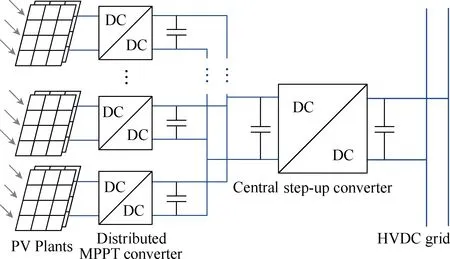
Fig.1 System configuration of the proposed HVDC grid-connected PV system

Fig.2 Centralized DC-DC converter with IPOS configuration
As is illustrated in Fig.1, the outputs of the distributed MPPT stage are gathered in the same transmission line to form a medium voltage direct current (MVDC) grid. Since the voltage of the MVDC grid is clamped by the HVDC side, the MPPT converter operates as a DC current source. Therefore, a simple control method can be adopted to regulate the output current. Several conventional DC-DC topologies, such as boost circuit, can be used to implement the MPPT stage. Multiple PV strings are connected to each converter to achieve a high power level. The centralized step-up DC-DC converter works as an interface between the MVDC grid and the HVDC side. It handles the current delivered by the MPPT stage with the voltage being imposed by the HVDC grid. Unlike the centralized PV inverter, output current regulation is not necessary for this stage. Therefore, the control scheme of the centralized stage is less complex than that of the traditional multi-modular DC-DC converter. As a result,it is possible for the centralized stage to be operated under open loop control as a simple power lever.
Comparing with the AC grid-connected system, the proposed HVDC conversion system can take the advantages of PV systems without low frequency AC link. Quantity and bulk of transmission lines can be reduced with less line loss. As power conversion stages are reduced significantly, system volume can also be saved and electricity generation can be improved.Therefore, the proposed system has the potential to decrease the system cost. It should be noted that several of the proposed conversion system can be connected easily to the same HVDC transmission line over large distances to form a multiple HVDC grid without steady issues like resonance in AC grid system.
In order to explain the architecture of the proposed conversion system, a detailed circuit implementation, as an example is introduced in the following.
2.1 Distributed MPPT stage
Conventional interleaved boost circuit can be employed as the distributed MPPT stage. A two phase boost circuit which is given in Fig.3 can be a candidate example. The boost converter is in charge of performing the MPPT algorithm of the attached PV strings and the power control of the conversion system. The interleaved operation reduces the input and output ripples of the stage greatly, allowing the reduction of the filters.

Fig.3 Interleaved boost topology of the MPPT module
As illustrated in Fig.1, the interleaved boost circuit converts the unstable PV voltage up to 1kV from 400.85kV which is common for most commercial large-scale PV systems. The power capacity of each converter depends on the PV array configuration of the system, which are usually 2060kW and limited by the capacity of power semiconductors and partial shading or mismatch of PV arrays.
The control scheme of the MPPT converter is shown in Fig.6, where MPPT and output power regulation are performed together in one controller.MPPT algorithms, such as incremental conductance and perturb and observe, are widely used in PV generation applications. In this study, incremental conductance method is employed. In the proposed system, the DC-DC step-up stage works under open loop, and thus,the system output power control is achieved by the MPPT stage. Instead of the current control of the high voltage side which suffers system bandwidth limitation and sampling precision issues under high voltage isolation conditions, output power of the MPPT stage is controlled in the proposed system.
Typical switching waveforms under steady-state operation of the MPPT module is shown in Fig.4(a). The interleaved boost topology has already been used and verified in the industrial PV systems. Design method and control algorithm are the same for the MPPT module in this paper. Number of interleaved phases and power capacity can be designed according to the applications. However, as hard switching is featured,switching frequency cannot be very high for the MPPT stage. As wide band-gap semiconductor devices attain outstanding properties such as higher breakdown voltage and lower on-resistance, better performance can be achieved by employing SiC MOSFETs for this stage.
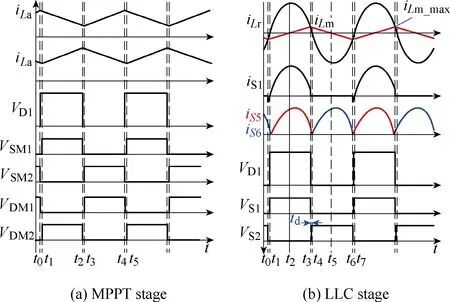
Fig.4 Steady-state waveforms of the proposed converter
2.2 Centralized DC-DC step-up stage
High frequency LLC topology is employed as a candidate example in the multi-modular step-up DC-DC stage. The LLC based modules decouples the MVDC side from the HVDC side with HF isolation. Interleaved technique can also be used for the multiple LLC cells. A detailed circuit scheme is shown in Fig.5. A full-bridge in primary side and a nature point clamp three level half bridge in secondary side are adopted for each module to achieve high voltage gain and high power capacity. Each cell is designed to be operated under one operation point with fixed switching frequency modulation to realize fixed gain and soft switching under the full load range.Therefore, high switching frequency can be used for the step-up DC-DC stage without significant switching loss.In steady-state conditions, the LLC module works under unregulated mode, that is open loop control, which means the switching frequency fsis equal to the resonant frequency. By adopting this control method, the LLC module has a constant voltage gain as a power amplifier.
Typical switching waveforms under steady-state operation of the LLC-based module is shown in Fig.4(b).The corresponding control scheme is illustrated in Fig.6.In the primary side, zero voltage switching(ZVS) is achieved for the switches during the dead-time, while zero current switching(ZCS) is achieved for the secondary side switches during the phase shift of the gate signals. To achieve high efficiency under the whole load range, adjustable dead-time and phase shift control are performed for the primary and secondary circuits simultaneously. In addition, as the LLC-based modules are configured as IPOS structure, self-balance can be achieved for the input voltage and output current without free-wheeling current.

Fig.5 High frequency LLC topology of the step-up conversion module
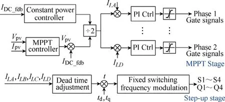
Fig.6 Control scheme of the proposed DC-DC conversion system
Unlike the traditional LLC resonant converter, the voltage gain under the point of fs= fris independent of the quality factor of the resonant tank. Moreover, the magnetizing inductor Lmhas little in fl uence on the voltage gain, which means that the design process of the resonant circuit can be simplified.
There are four main states and eight main states for the boost stage and the LLC stage during one switching cycle, respectively, as depicted in Fig.4a and Fig.4b. As with the interleaved operation of the boost phases, input and output ripples can be decreased. Smaller filters can be employed to improve the power density. Because of the resonant operation of the whole operation range, the LLC stage can achieve zero-voltage-switching(ZVS) for the primary side switches and zero-current-switching(ZCS) for the secondary side switches. Higher switching frequency can be adopted to achieve high efficiency and high power density.
The basic control strategy of the proposed module is shown in Fig.6. The boost stage operates on the same principle as the conventional continues-current-mode(CCM) boost circuit. As the input of the converter is PV power, maximum power point tracking(MPPT) control is required. Conventional MPPT strategy can be employed. In addition, for the PV HVDC integrated system applications, the proposed converter is designed to connect and deliver power to the HVDC grid as a current source. Therefore, unlike the conventional voltage source type, the boost stage is handled as a current source converter. As shown in Fig.6, close loop of the DC bus current control is employed for the boost converter.
In ideal conditions, the LLC resonant stage works under unregulated mode, which means the switching frequency fsis equal to the resonant frequencyTherefore, the ideal LLC converter has a constant voltage gain as an ideal power amplifier.However, in practical applications, the actual resonant frequency fsof the LLC converter cannot be determined accurately. The nonlinear parasitic parameters of the circuit can affect the inherent fs. Lrand Cralso drift under different load or temperature conditions, which cannot be avoided especially in high power and high voltage applications. Moreover, DC bus voltage will increase under heavy load conditions because the voltage drop across the circuit increases with the current increase. Therefore, frequency close loop control is necessary to compensate as illustrated above. As the drift of the voltage is minimal compared with the DC link voltage, narrow switching frequency modulation is adopted for the LLC resonant circuit. This characteristic facilitates the design of the magnetic elements for reducing losses and design complexity. In addition, the bandwidth of the frequency control loop can be relatively low compared with that of the actual output regulation loop, as the voltage drift rate is slow.
Since the LLC stage is regulated in a very narrow frequency range to compensate the DC bus voltage slightly, the output current regulation is carried out mainly by the boost stage. In the actual design, the DC bus current IDCis controlled instead of the LLC output current Io. Regulation of IDC, as well as the MPPT control,is realized by controlling the duty ratio of switches SM1and SM2. Therefore, highly dynamic response control can be realized. Moreover, feedback signal problems because of the high voltage electrical insulation can be eliminated. This also results in the converter operating as a power lever, where high voltage output is controlled by the low DC bus voltage automatically.
Unlike the traditional LLC resonant converter, the voltage gain under the point of fs= fris independent of the quality factor of the resonant tank. Moreover, the magnetizing inductor Lmhas little in fl uence on the voltage gain, which means that the design process of the resonant circuit can be simplified. As a result, Lmcan be designed as large as possible to reduce the conduction loss. For the LLC stage, all the primary and secondary switches are softly switched over the full load range,which significantly decreases the switching loss.
3 Analysis and design
3.1 Voltage gain of the proposed converter
By investigating the detailed operation, the voltage conversion ratio of the boost stage can be obtained as follows

where D is the duty cycle of SM1and SM2.
The analysis of the LLC stage is based on the simplified equivalent circuit as shown in Fig.7, where Ceqis the equivalent capacitor of the main switches.During the dead-time of the transition, Ceqcan be obtained as

where Cds_pridenotes the equivalent output capacitor of the primary side switches and Cds_secis the equivalent capacitor of the secondary switch.
The voltage conversion ratio of the LLC converter can be derived from Fig.7 as

Therefore, the voltage gain of each module is


Fig.7 Equivalent circuit of LLC stage
If the LLC stage operates at the ideal point fs= fr, Mmodulecan be simplified as

It can be seen that the conversion ratio of the proposed module is a function of duty cycle D and transformer turn ratio n. By adjusting the turn ratio n, high conversion ratio can be achieved.
As a result, the voltage step-up ratio of the proposed IPOS converter can be expressed as

where N is the number of the active modules.
3.2 Design considerations of the LLC converter
As discussed above, the design method of the LLC stage under very narrow switching frequency range is different than with the traditional LLC converter. The main design principle of the LLC stage is to accomplish the soft switching conditions for all switches under the full range of loads. Assuming all the elements of the circuit are ideal, to satisft the soft switching conditions,the maximum current of the magnetizing inductor,iLm_max, should be large enough to charge and discharge the equivalent output capacitors of the switches during the deadtime td. Therefore, Lmcan be designed as

Large Lmwill result in a small magnetizing current. In order to minimize the conduction loss in the primary side, Lmshould be selected as large as possible. However,Lmcan also limits the voltage gain of the converter, as shown in Fig.8. As a result, Lmshould be decided by (7)and maximum voltage gain requirement of the converter.
The voltage conversion ratio of the LLC stage with different Q values is depicted in Fig.9. There are three regions during the switching frequency range. The voltage conversion ratio is almost fixed to unity at the resonant frequency frregardless of the load condition.As fsincreases in up ZVS region fs>fr, the voltage gain decreases. However, in the region of fs<fr, the normalized voltage gain can be higher or lower than unity according to different Q values. To accomplish the soft-switching conditions, LLC should always work under ZVS region. Therefore, there exists a maximum Q value in the boundary of ZVS region and ZCS region.According to (8), the maximum value of Lrcan be derived. Meanwhile, to compensate the voltage drift effectively, narrow fsrange should be guaranteed, which is also a benefit for the transformer design. Therefore, k= Lm/Lrshould be as small as possible. However, small k results in large Lr, which means large magnetics. The voltage gain curves of the LLC stage with different Lrvalues is depicted in Fig.10. For a large Lr, the gain of the converter is limited. Therefore, Lrshould be selected according to the voltage gain requirement and Q conditions.

Fig.8 Voltage gain curves for different values of Lm when VDC=100V, V0 = 400V, Lr=25µH, fr =100kHz, and RL=53Ω

Fig.9 Voltage gain curves for different values of Q when Lm= 360µH, Lr = 25µH, and fr = 100kHz

According to Fig.7, the rms value of the resonant current can be expressed as

Therefore, the maximum voltage across the resonant capacitor Cris obtained as
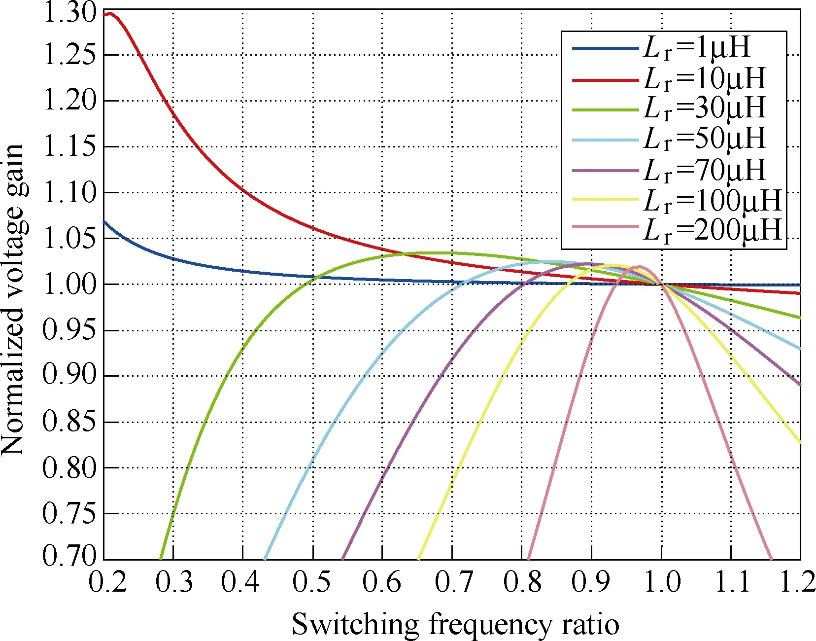
Fig.10 Voltage gain curves for different values of Lr when Lm=360µH, fr = 100kHz, and RL =53Ω

which is the limitation of Crselection, especially in high voltage applications.
Therefore, (7)~(10) result the design principle of the resonant tank. Based on this principle, several trade-offs should be carried out.
4 Simulation and experimental results
4.1 Simulation results
In order to verify the analysis, a PSIM simulation circuit of the module for the proposed converter has been developed. The basic structure of the system is shown in Fig.11. Two interleaved converters were employed to act as the MPPT stage. A full-bridge LLC converter was used to act as the centralized stage. Two DC voltage sources were employed as the input PV arrays. The key parameters are summarized in Table1.
Fig.12 illustrates the key waveforms of the LLC stage. The circuit is simulated under the rated load with the input voltage of 80V and output voltage of 400V. It can be seen that the primary side switches, S1~S4,operate under ZVS conditions during the deadtime of the driver signals. The secondary side switches, S5~S8,which act in synchronous rectification mode, operate under ZCS conditions. As a result, high switching frequency with minimum switching losses can be achieved for the LLC stage.
4.2 Experimental results
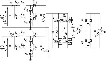
Fig.11 System structure of the simulation and prototype circuit
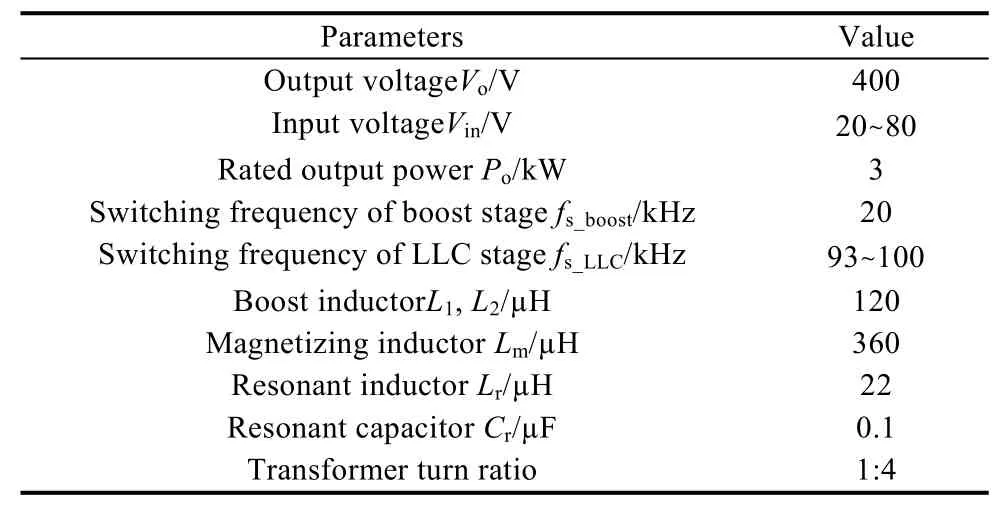
Table 1 Key parameters of the proposed module

Fig.12 Simulation waveforms of the LLC-based step-up module
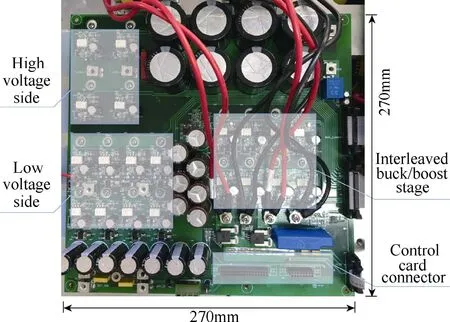
Fig.13 Experimental prototype circuit
A 3kW experimental prototype circuit of the proposed module has been built and tested, as shown in Fig.13. The circuit specifications are the same as those for the simulation described in Table 1. To achieve high power density and high efficiency, SiC MOSFETs C3M0120090D were adopted for the high voltage side switches. In Fig.13, high frequency transformer and inductors were arranged in the back side with the heatsink. A final size of 270mm×270mm×40mm and power density of 1.0W/cm3ware achieved for the proposed module.
The experimental results of the boost stage as well as the LLC stage under full load condition are shown in Fig.14 and Fig.15, with the input voltage of 50V and output voltage of 400V. It can be seen that the input current ripple is decreased significantly because of the interleaved operation for the two phases. As the fullload-range soft-switching characteristic of the LLC stage,much higher switching frequency can be adopted to achieve high power density without significant power loss.
Fig.16 shows the operation waveforms of the LLC stage under the rated load. It can be seen that the circuit performs resonant operation under fs=frcondition. The power fl ow of the circuit is controlled by the buck/boost stage. In addition, the DC bus voltage is controlled to be constant also by the buck/boost stage. According to the waveforms of iLr, is, and Vcd, the primary side switches are well operated under ZVS condition, and the secondary side switches are operated under ZCS conditions, which is the same as the simulation results.
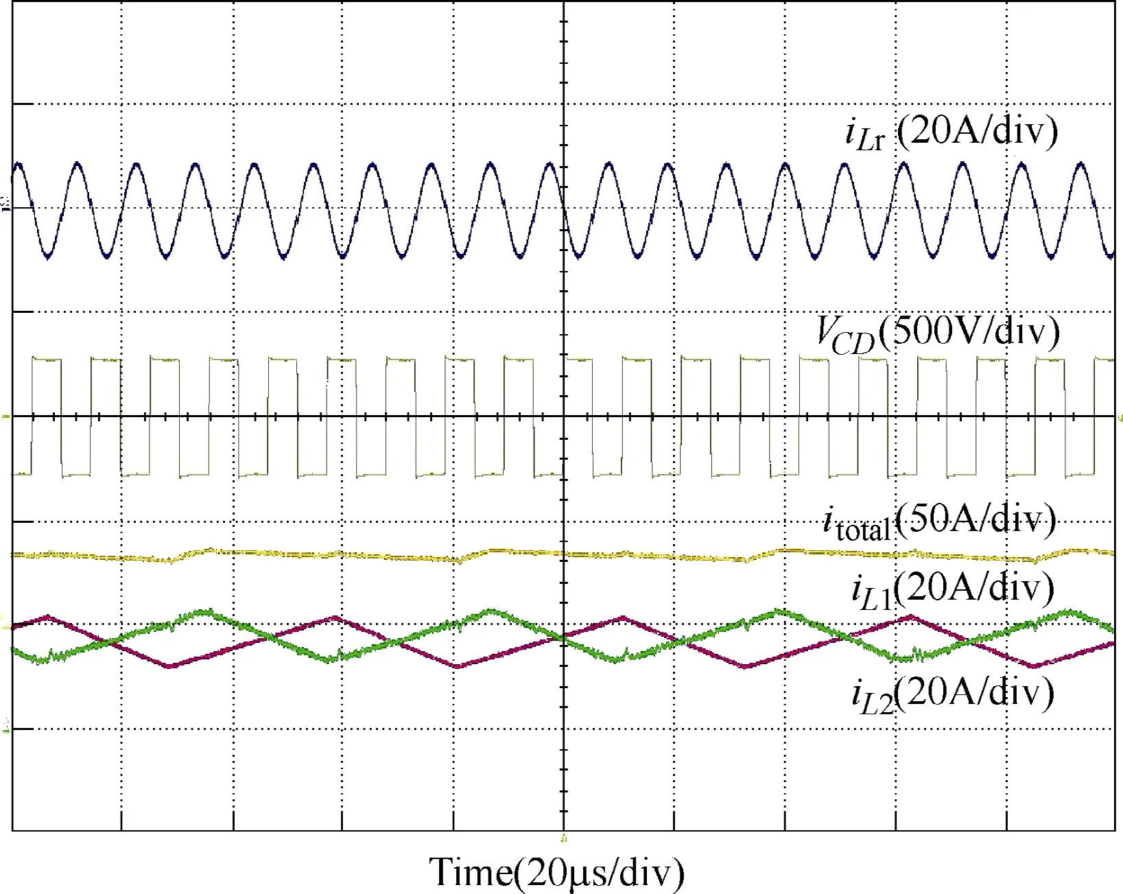
Fig.14 Experimental waveforms of the proposed converter under rated load
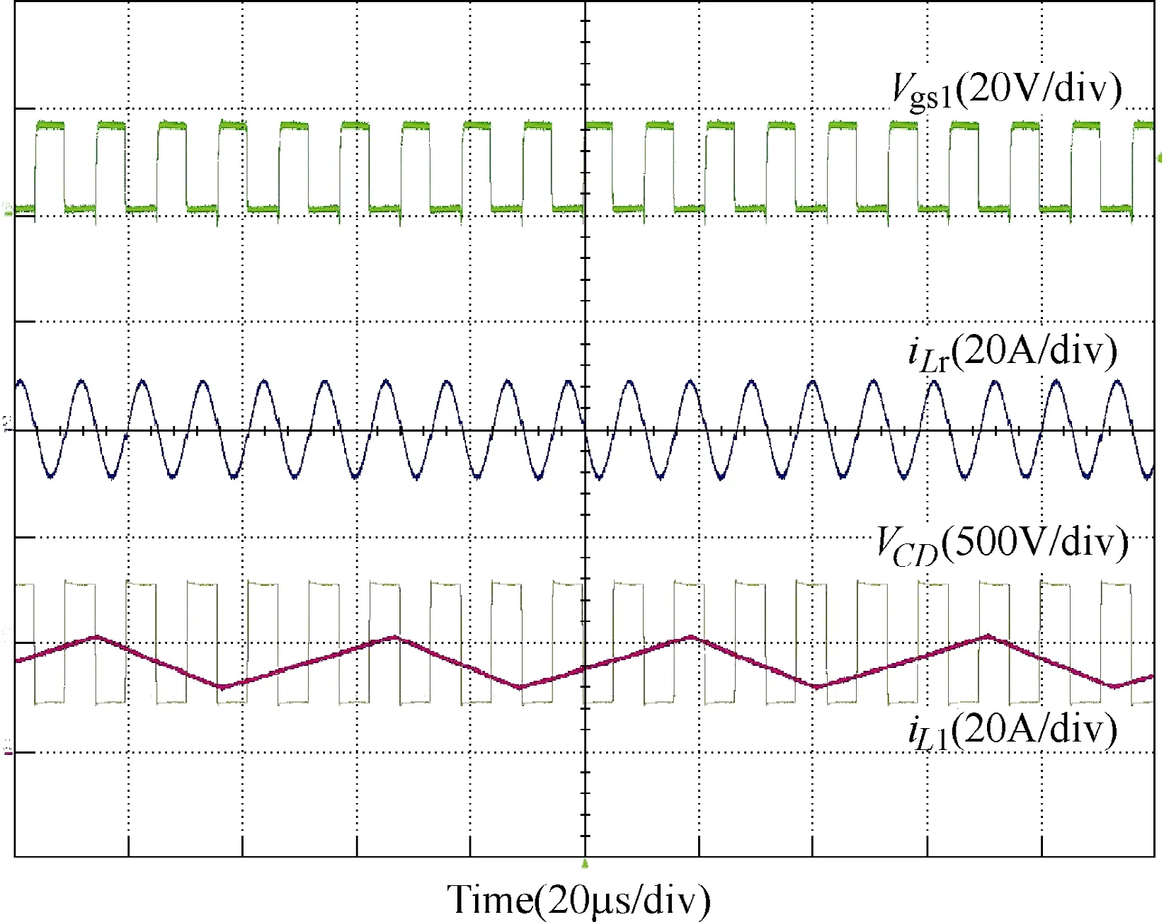
Fig.15 Experimental waveforms of the proposed converter under rated load

Fig.16 Experimental waveforms of the LLC stage under rated load
As discussed before, the inherent resonant frequency of the LLC circuit may change because of the parasitic parameters and the in fl uence of load and temperature conditions. If fixed frequency control is adopted in the LLC stage, the operating-point may shift to the ZCS region shown in Fig.9. This problem can affect the stability and efficiency of the circuit, which can be seen in Fig.16. To compensate the voltage drift under different conditions, the maximum frequency under light load is 100kHz. As the load increasing, the switching frequency is modulated to 95kHz.
Fig.17 and Fig.18 shows the detailed switching waveforms of the LLC-based module under the resonant frequency and rated load. ZVS turn-on and turn-off are achieved simultaneously for the circuit, as it takes the advantage of open loop controlled LLC converter.Therefore, for the centralized step-up stage, switching losses can be minimized.
Fig.19 shows the switching waveforms of the LLC-based voltage step-up module under full load conditions. It can be seen that the circuit performs resonant operation under fs= frcondition, as the power flow of the circuit is controlled by the MPPT stage. The DC bus voltage, which simulates the HVDC grid, is clamped to be constant by the high side high voltage source. According to the waveforms of iLr, is, and Vcd,the primary side switches are well operated under ZVS condition, and the secondary side switches are operated under ZCS conditions synchronously, which is the same as the simulation results.
As discussed before, the inherent resonant frequency of the LLC circuit may change because of the parasitic parameters and the in fl uence of load and temperature conditions. If fixed frequency control is adopted in the LLC stage, the operating-point may shift to the ZCS region shown in Fig.9. This problem can affect the stability and efficiency of the circuit, which can be seen in Fig.16. To compensate the voltage drift under different conditions, the maximum frequency under light load is 100kHz. As the load increasing, the switching frequency is modulated to 95kHz(seen in Fig.20).
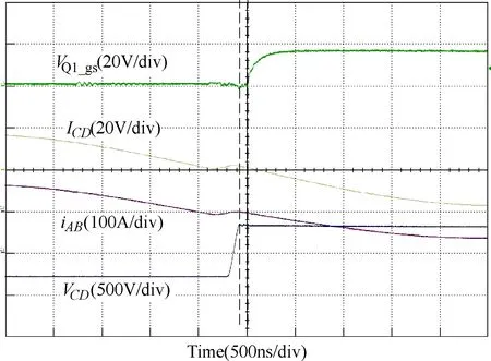
Fig.17 ZVS turn-on waveforms of the LLC based step-up modular

Fig.18 ZVS turn-off waveforms of the LLC-based step-up module
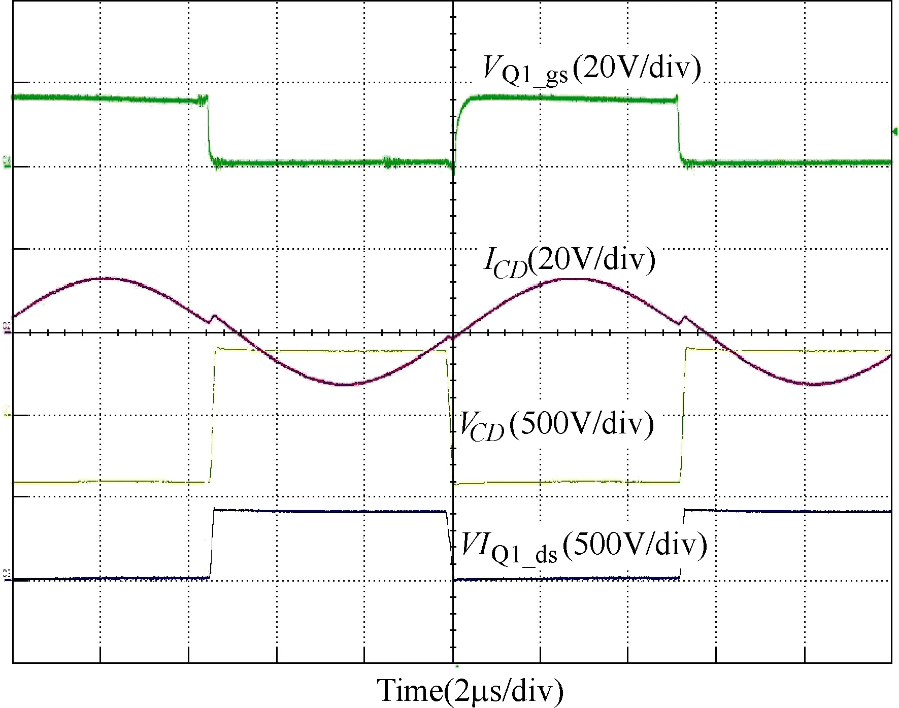
Fig.19 Experimental waveforms of the LLC-based step-up module under rated load
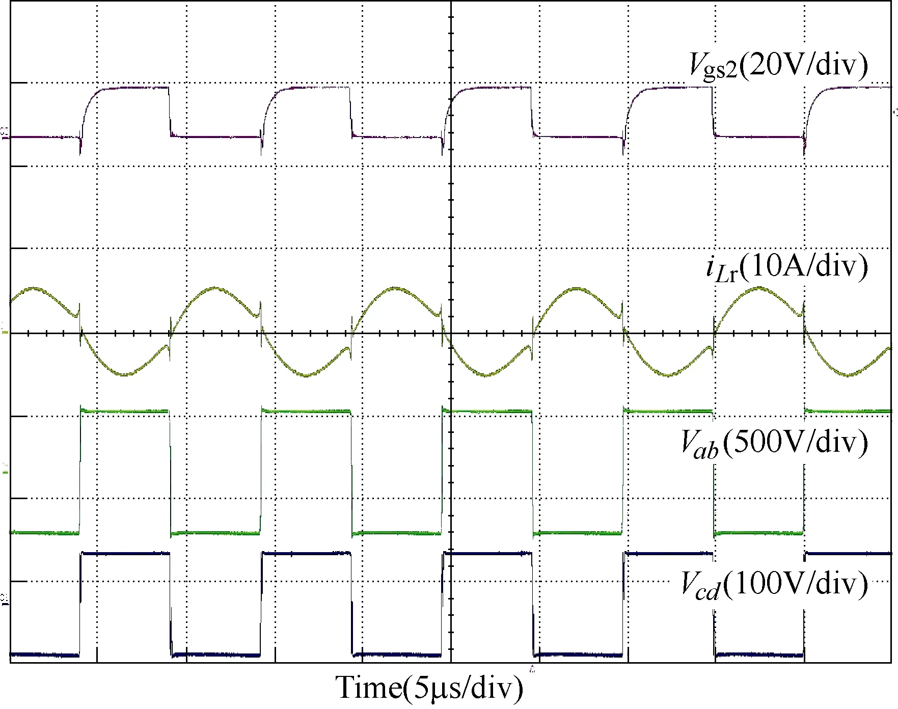
Fig.20 Resonant frequency drift of the LLC stage
Fig.21 shows the measured system efficiency for converter operating in boost mode from 10% load to full load. It can be seen that high efficiency is achieved for the wide load range. The maximum efficiency for the converter is 93.2%.
5 Conclusions

Fig.21 System efficiency of the proposed module
A modular DC/DC system with distributed MPPT stage and centralized voltage step-up stage for PV energy integrated into HVDC grids is proposed in this paper. By employing distributed MPPT stage, high power losses caused by partial shading of the PV arrays are reduced significantly. Modular scheme is adopted for the centralized step-up DC-DC stage. The modules are configured as IPOS structure and designed as open-loop controlled LLC converters. A detailed realization of the proposed system and design consideration has been carried out. A 3kW prototype circuit is built to validate the theoretical analysis and feasibility of the proposed converter.
 Chinese Journal of Electrical Engineering2018年2期
- Chinese Journal of Electrical Engineering的其它文章
- Brushless Doubly-Fed Machines:Opportunities and Challenges
- Control and Applications of Direct Matrix Converters: A Review
- An Optimal Charging/Discharging Strategy for Smart Electrical Car Parks
- Two-Stage Transformerless Dual-Buck PV Grid-Connected Inverters with High Efficiency
- A New Active Gate Driver for MOSFET to Suppress Turn-Off Spike and Oscillation
- Dual-Coupled Robust Wireless Power Transfer Based on Parity-Time-symmetric Model
