
掺镁氧化锌薄膜结构及其光学性质的研究
2017-04-15 02:01钟志有
中南民族大学学报(自然科学版) 2017年1期
钟志有, 康 淮, 陆 轴, 龙 路
(中南民族大学 电子信息工程学院, 智能无线通信湖北省重点实验室, 武汉 430074)
掺镁氧化锌薄膜结构及其光学性质的研究
钟志有, 康 淮, 陆 轴, 龙 路
(中南民族大学 电子信息工程学院, 智能无线通信湖北省重点实验室, 武汉 430074)
以氧化镁(MgO)掺杂的氧化锌(ZnO)陶瓷靶作为溅射靶材,采用射频磁控溅射方法在玻璃衬底上制备了掺镁ZnO(ZnO:Mg)薄膜样品.通过X射线衍射仪和可见-紫外光分光光度计的测试表征,研究了溅射时间对ZnO:Mg薄膜晶体结构和光学性质的影响.结果表明:ZnO:Mg薄膜的结构和性能与溅射时间密切相关.随着溅射时间的增加,ZnO:Mg薄膜(002)晶面的织构系数减小、(110)晶面的织构系数增大,对应的可见光波段的平均透过率降低.溅射时间为15 min时,ZnO:Mg薄膜样品具有最佳的(002)择优取向生长特性和最好的透光性能.同时ZnO:Mg薄膜样品的禁带宽度随溅射时间增加而单调增大.与未掺杂ZnO薄膜相比,所有ZnO:Mg薄膜样品的禁带宽度均变宽.
磁控溅射;氧化锌;晶体结构;光学性质
作为一种新型的Ⅱ-Ⅵ族直接带隙半导体材料,氧化锌(ZnO)可以广泛应用于太阳能电池[1-5]、发光二极管[6-9]、光波导器件[10]、平板显示[11-15]、气体传感器[16-18]以及窗口材料[19]等众多领域,同时由于它具有禁带宽、原料丰富、无毒性、价格低廉等潜在优势,被普遍认为是传统铟锡氧化物(ITO)的最佳替代品之一[20-22],因此深受国内外科技界和工业界的广泛关注.人们通过在ZnO中掺入杂质可以改变其特性,以满足特殊用途的需要.例如:掺镉ZnO能够调节薄膜的禁带宽度,应用于光热转换太阳能器件之中,掺铍ZnO能够增强薄膜的电学稳定性,掺锆ZnO能够提高薄膜的热稳定性,而掺铝ZnO则有利于改善薄膜的综合光电性能[23-25].目前,在ZnO中掺入Mg成分形成三元合金Zn1-xMgxO,使之禁带宽度比纯ZnO的大,并且可以通过调节Mg/Zn不同原子比来获得不同的禁带宽度.Zn1-xMgxO作为一种新的光电材料,由于其禁带宽度较大且可调控,因此它在半导体激光器、ZnO/Zn1-xMgxO超晶格、异质结、量子阱等光学带隙工程中,具有巨大的应用潜力.此外,在CIGS薄膜太阳能电池中,Zn1-xMgxO薄膜也被很多研究者视为替代有毒CdS作为缓冲层极具前景的材料之一[19].因此,对于掺镁ZnO(ZnO:Mg)薄膜制备和性质的研究具有极其重要的意义.
ZnO:Mg薄膜的制备方法主要有磁控溅射沉积[26-30]、脉冲激光沉积[31,32]、原子层沉积[33,34]、喷雾热分解[35,36]、溶胶-凝胶法[37,38]等,而其中采用射频磁控溅射技术制备ZnO:Mg薄膜具有沉积速率高、均匀性好、粘附性能好、便于大批量工业生产等优势[39-42],所以获得了广泛应用.本文以普通玻璃为衬底材料,以MgO掺杂的ZnO陶瓷靶作为溅射靶材,采用射频磁控溅射技术制备ZnO:Mg薄膜样品,通过X射线衍射仪、紫外-可见光分光光度计等测试表征,研究了溅射时间对ZnO:Mg薄膜晶体结构及其光学性质的影响.
1 实验部分
1.1 衬底处理
选用厚度为1 mm的普通玻璃作为衬底材料,衬底大小为30 mm×30 mm.实验前首先对玻璃衬底进行擦拭、冲洗,然后依次在丙酮溶液、无水乙醇和去离子水中进行超声清洗15 min,最后使用去离子水冲洗并自然干燥,放入预溅射室中.
1.2 样品制备
ZnO:Mg薄膜样品通过射频磁控溅射方法制备,所用成膜设备为沈阳科友真空设备公司生产的KDJ-567型高真空磁控与离子束复合镀膜系统,所用射频频率为13.56 MHz.系统的本底真空度为2.8×10⁻⁴Pa,衬底温度为300 ℃,溅射功率为180 W,溅射时间为15~25 min,所用陶瓷靶材为合肥科晶材料技术有限公司生产,由纯度均为99.99%的ZnO和MgO(两者的质量比为97%:2%)经过高温烧结而成,靶材直径为50 mm,厚度为4 mm,靶材与衬底之间的距离为75 mm.溅射时所用工作气体为99.999%的高纯氩气,溅射时氩气压强为2.3 Pa.实验过程中,保持其它工艺参数不变而改变溅射时间,分别将溅射时间设置为15、20和25 min制备薄膜样品,以研究溅射时间对ZnO:Mg薄膜样品晶体结构及其光学性质的影响.
1.3 样品测试
ZnO:Mg薄膜样品的晶体结构通过德国Bruker公司的D8-ADVANCE型X射线衍射仪(Cu Kα,射线源的波长λ=1.5406 Å)分析,采用θ-2θ连续扫描方式,扫描速度为10 °/min,扫描步长为0.0164°,工作电压为40 kV,工作电流为40 mA.扫描角度为30°~70°.光学透过率利用北京普析通用仪器公司的UV-2100型双光束紫外-可见分光光度计进行表征,测量时扫描步长为1 nm,扫描范围为300~800 nm.所有测试均在室温和大气条件下完成.
2 结果与讨论
2.1 薄膜的生长速率
不同溅射时间时ZnO:Mg薄膜样品的厚度如图1所示,可以看出,溅射时间为15、20和25 min时,ZnO:Mg薄膜样品的厚度分别为550、890和1060 nm,对应的薄膜生长速率为0.61、0.74和0.71 nm/s.很明显,在制备薄膜样品的初始阶段,其生长速率相对较小;随着溅射时间的增加,薄膜生长速率也有所有增大,但是当溅射时间增加到一定程度之时,薄膜的生长速率却略有减小.可见,在ZnO:Mg薄膜制备过程中,其生长速率的变化幅度较小,它随溅射时间的增加而呈现出先增大后减小的变化趋势.

图1 不同溅射时间时薄膜样品的厚度Fig.1 Thickness of the thin films deposited with various sputtering time
2.2 薄膜的晶体结构
不同溅射时间时ZnO:Mg薄膜样品的XRD图谱如图2所示,从图中可知,在30°~70°的扫描范围内,所有的ZnO:Mg薄膜样品都显示有三个强度较大的XRD衍射峰,分别位于2θ为31°、34°和55°附近,通过比对标准ZnO晶体(JCPDS No.36-1451)[43,44]发现它们分别与ZnO晶面(100)、(002)和(110)的特征谱线数据相吻合.另外,XRD图谱中并没有出现金属Zn、金属Mg以及MgO的特征衍射峰,其测试结果表明:在实验制备的薄膜样品中,Mg替代了Zn的位置,或者存在于六角晶格之中,或者分布在晶粒间界的区域,所有ZnO:Mg薄膜样品具有ZnO六角纤锌矿型结构,并且它们均为多晶薄膜.

图2 薄膜样品的XRD图谱Fig.2 XRD patterns of the thin films
不同溅射时间时,ZnO:Mg薄膜样品各个晶面的衍射峰强度(I(100)、I(002)、I(110))如图3所示,可以看出,随着溅射时间的增加,I(100)、I(002)和I(110)呈现出不同的变化趋势,其中,I(002)随溅射时间增加而单调减小、I(110)随溅射时间增加而单调增大,而I(100)随溅射时间增加则先增大而后减小.为了表征所制备ZnO:Mg薄膜样品的择优取向特性,本文采用织构系数(TC(hkl))进行定量描述.织构系数TC(hkl)定义为某个晶面的相对衍射强度与各晶面相对衍射强度总和的平均值之比[45],其具体表达式如下:
(1)
(1)式中,N为计算时所取的晶面总数目;h、k、l为衍射晶面密勒指数;TC(hkl)表示(hkl)晶面的织构系数;I(hkl)和I0(hkl)分别为薄膜样品与标准ZnO试样(JCPDS No.36-1451)在(hkl)晶面的衍射峰强度.在本文中,N=3,即取三个较强的衍射峰(100)、(002)和(110)来计算TC(hkl).从公式(1)看出:如果各个衍射面的TC值都相同时,就说明各晶面的取向是无序的;如果某个晶面的TC值大于1时,则表示该晶面表现出择优生长取向特性,同时TC的数值越大,则表明择优取向的程度就越高.
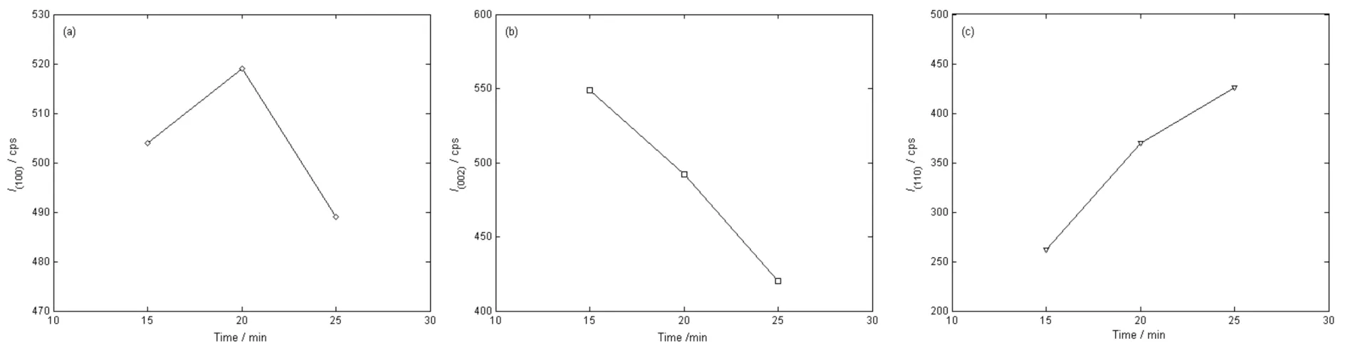
图3 薄膜样品的衍射峰强度Fig.3 The intensity of diffraction peaks for the thin films
根据图3中ZnO:Mg薄膜样品的XRD分析数据,可以计算出不同溅射时间时ZnO:Mg薄膜样品在(100)、(002)和(110)晶面的织构系数TC(hkl),其结果如图4所示.由图可知,对于所制备的ZnO:Mg薄膜样品,其TC(100)值为0.61~0.68、TC(002)值为0.95~1.35,而TC(110)值为0.97~1.45.可以看出,TC(100)值的变化幅度很小,几乎不受溅射时间的影响;而TC(002)值和TC(110)值的变化幅度较大,说明它们明显受到溅射时间的影响.从图4中还看到,TC(100)的数值均小于1,并随溅射时间增加而单调减小,这说明ZnO:Mg薄膜没有显示(100)晶面择优取向生长特性.当溅射时间从15 min增加到25 min时,TC(002)和TC(110)呈现出相反的变化趋势,即TC(002)值从1.35减小为0.95,而TC(110)值则从0.97增大为1.45,可见,溅射时间为15 min时ZnO:Mg薄膜的择优取向为(002),溅射时间为20 min时ZnO:Mg薄膜的择优取向为(002)和(110),而溅射时间为20 min时ZnO:Mg薄膜的择优取向为(110).这一结果表明:ZnO:Mg薄膜的择优取向生长特性是随溅射时间而改变的.
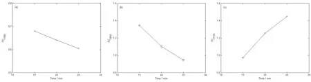
图4 薄膜样品的织构系数Fig.4 The texture coefficient of (hkl) plane of the thin films
根据XRD测试数据,不同溅射时间时ZnO:Mg薄膜样品的平均晶粒尺寸(D)可以利用由Scherrer公式[46,47]进行计算:
(2)
(2)式中,K为由Scherrer常数,其值为0.89;λ为XRD测试时所使用的X射线源的波长(λ=0.15406 nm);B为择优取向生长衍射峰的半高宽.θ为所对应衍射峰晶面的布柆格角.图5给出了不同溅射时间时ZnO:Mg薄膜样品的平均晶粒尺寸D.由图可见,平均晶粒尺寸D约为10.3~10.7 nm,其变化幅度为0.4 nm.这一结果表明:在本实验中ZnO:Mg薄膜的平均晶粒尺寸几乎不受溅射时间的影响.
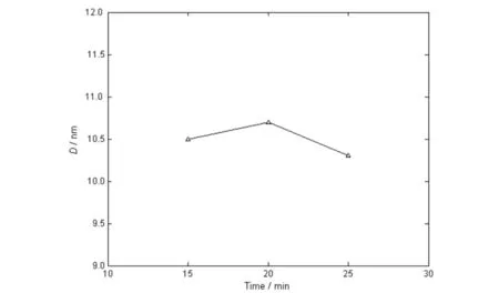
图5 薄膜样品的平均晶粒尺寸Fig.5 Average grain size of the thin films
2.3 薄膜的光学性质
图6为不同溅射时间时ZnO:Mg薄膜样品的透过率曲线,为了方便比较,图中还增加了未掺杂ZnO薄膜样品的透过率曲线,如图6(a)所示,其制备工艺条件与溅射时间为15 min时ZnO:Mg薄膜的工艺参数完全相同.从图中看出,与未掺杂ZnO薄膜样品相比,所有ZnO:Mg薄膜样品的截止波长均向短波方向移动,即出现“蓝移”现象,溅射时间增加则“蓝移”越大,这说明ZnO:Mg薄膜样品的禁带宽度均大于未掺杂ZnO薄膜的数值,并且随溅射时间的增加而增大.从图中还可以看出,所有薄膜样品的透过率曲线都显示了清晰、光滑的干涉条纹,这说明所实验所制备的薄膜样品厚度是均匀的、表面是平整的.当溅射时间增加时,薄膜样品的干涉条纹就越多.这是由于溅射时间增加时,所沉积薄膜的厚度也会随之增加的缘故.

图6 薄膜样品的透过率曲线Fig.6 Transmittance spectra of the thin films
对于未掺杂ZnO薄膜样品,在可见光区域的平均透过率Tav为82.9%,具有较好的透光性.图7为不同溅射时间时ZnO:Mg薄膜样品在可见光波段的平均透过率(Tav),由图可见,ZnO:Mg薄膜的平均透过率Tav与溅射时间成反变关系,当溅射时间为15、20和25 min时,ZnO:Mg薄膜的Tav值分别为90.2%、88.9%和88.1%,其Tav值明显高于未掺杂ZnO薄膜样品,表现出优良的透光性能.由此可见,镁掺杂有利于提高ZnO薄膜的透光性能.
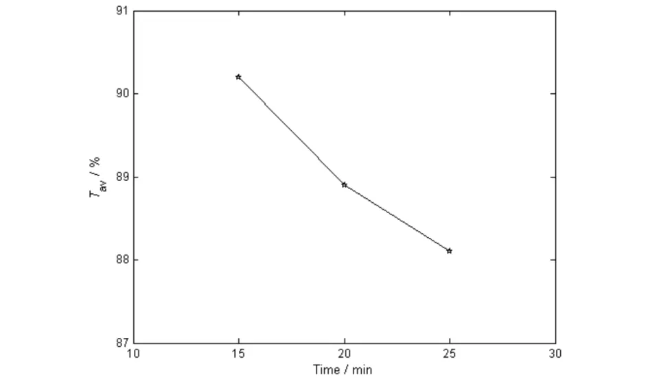
图7 薄膜样品的可见光波段平均透过率Fig.7 Average transmittance in the visible light range of thin films
在吸收边附近,ZnO:Mg薄膜的透过率(T)与吸收系数(α)之间满足如下关系式[48]:
T=T0e-αd,
(3)
式(3)中,d为薄膜厚度;T0为常数,在吸收边附近T0≈1,因此,利用公式(3)由薄膜厚度d以及对应的吸收边附近的光学透过率T就可以计算薄膜的吸收系数α.根据Tauc公式[49,50],在薄膜的吸收边附近,吸收系数α与入射光子能量(hv)之间满足如下方程:
(αhv)n=C0(hv-Eg),
(4)
式(4)中,C0为常数,Eg为薄膜的禁带宽度,指数n的值取决于光子跃迁的类型.当n=2时,对应于直接跃迁,而当n=1/2时则对应于间接跃迁[48].由于ZnO:Mg薄膜属于直接跃迁材料,故取n=2作出(αhv)2与hv之间的关系曲线图,根据外推法得到横轴(hv)上的交点(αhv=0)后,可以获得薄膜的禁带宽度Eg.图8为未掺杂ZnO薄膜和不同溅射时间时ZnO:Mg薄膜样品的(αhv)2-hv关系曲线,利用外推法可得:未掺杂ZnO样品的Eg值为3.202 eV,而ZnO:Mg薄膜样品的Eg值为3.320~3.335 eV(见图9),均大于未掺杂ZnO薄膜的禁带宽度(3.202 eV),这是由于Mg掺杂后周围电子能量增大产生的高能级与Burstein-Moss效应[51,52]共同作用的结果.

图8 薄膜样品的(αhν)2-hν关系曲线Fig.8 The (αhν)2-hν curves of the thin films

图9 薄膜样品的禁带宽度Fig.9 Band gaps of the thin films
3 结语
采用MgO掺杂ZnO高密度陶瓷靶作为溅射靶材料,利用射频磁控溅射工艺在玻璃衬底上制备了ZnO:Mg薄膜样品,研究了溅射时间对ZnO:Mg薄膜晶体结构和光学性能的影响.研究结果表明:所制备的ZnO:Mg样品均为六角纤锌矿型的多晶结构,其晶粒生长特性和光学性能与溅射时间密切相关.溅射时间增加时,ZnO:Mg薄膜样品的TC(002)值减小而TC(110)值增大,对应的可见光区平均透过率降低.当溅射时间为15 min时,ZnO:Mg样品的(002)择优取向生长特性最好、平均透过率最高(90.2%).另外,利用外推法获得了ZnO:Mg薄膜的禁带宽度,结果表明:溅射时间对ZnO:Mg薄膜禁带宽度具有一定的影响,由于Mg掺杂后周围电子能量增大产生的高能级与Burstein-Moss效应共同作用从而使ZnO:Mg薄膜的禁带宽度有所增加.
[1] Lee D,Bae W K,Park I,et al.Transparent electrode with ZnO nanoparticles in tandem organic solar cells [J].Sol Energy Mater Sol Cells,2011,95(1): 365-368.
[2] Kim J Y,Lee K,Coates N E,et al.Tandem polymer solar cells fabricated by all-solution processing [J].Science,2007,317(5835): 222-225.
[3] Bekci D R,Erten-Ela S.Effect of nanostructured ZnO cathode layer on the photovoltaic performance of inverted bulk heterojunction solar cells [J].Renewable Energy,2012,43(2): 378-382.
[4] Sio A D,Chakanga K,Sergeev O,et al.ITO-free inverted polymer solar cells with ZnO:Al cathodes and stable top anodes [J].Sol Energy Mater Sol Cells,2012,98(1): 52-56.
[5] 肖健平,何 青,陈亦鲜,等.CIGS薄膜材料研究进展 [J].西南民族大学学报(自然科学版),2008,34 (1): 189-193.
[6] Kim H,Horwitz J S,Kim W H,et al.Doped ZnO thin films as anode materials for organic light-emitting diodes [J].Thin Solid Films,2002,420-421(1): 539-543.
[7] Cao H T,Sun C,Pei Z L,et al.Properties of transparent conducting ZnO:Al oxide thin films and their application for molecular organic light-emitting diodes [J].J Mater Sci: Mater Electron,2004,14(1): 169-174.
[8] Kim H,Piqué A,Horwitz J S,et al.Effect of aluminum doping on zinc oxide thin films grown by pulsed laser deposition for organic light-emitting devices [J].Thin Solid Films,2000,377-378(1): 798-802.
[9] Wang L,Swensen J S,Polikarpov E,et al.Highly efficient blue organic light-emitting devices with indium-free transparent anode on flexible substrates [J].Org Electron,2010,11(6): 1555-1560.
[10] Ozgur U,Alivov Y I,Liu C,et a1.A comprehensive review of ZnO materials and devices [J].J Appl Phys,2005,98(4): 041301-041301-103.
[11] Yamamoto N,Makino H,Osone S,et al.Development of Ga-doped ZnO transparent electrodes for liquid crystal display panels [J].Thin Solid Films,2012,520(11): 4131-4138.
[12] Tang C W,VanSlyke S A.Organic electroluminescent diodes [J].Appl Phys Lett,1987,51(12): 913-915.
[13] Burroughes J H,Bradley D D C,Brown A R,et al.Light-emitting diodes based on conjugated polymers [J].Nature,1990,347(6293): 539-541.
[14] Zhong Z Y,Jiang Y D.Surface treatments of indium-tin oxide substrates for polymer electroluminescent devices [J].Phys Status Solidi A,2006,203(15): 3882-3892.
[15] You Z Z,Hua G J,Lou S F.Optoelectrical characteristics of organic light-emitting devices fabricated with different cathodes [J].Int J Electron,2011,98(1): 129-135.
[16] Patel N G.,Patel P D,Vaishnav V S.Indium tin oxide (ITO) thin film gas sensor for detection of methanol at room temperature [J].Sensor Actuat B-Chem,2003,96(1-2): 180-189.
[17] Yi I-J,Kim J-H,Choi Y J,et al.A disposable biosensor with Prussian blue deposited electrode [J].Microelectron Eng,2006,83(4-9): 1594-1597.
[18] Mitsubayashi K,Wakabayashi Y,Tanimoto S,et al.Optical-transparent and flexible glucose sensor with ITO electrode [J].Biosens Bioelectron,2003,19(1): 67-71.
[19] 叶志镇,吕建国,张银珠,等.氧化锌半导体材料掺杂技术与应用 [M].杭州: 浙江大学出版社,2009.
[20] Park S,Tark S T,Lee J S,et al.Effects of intrinsic ZnO buffer layer based on P3HT/PCBM organic solar cells with Al-doped ZnO electrode [J].Sol Energy Mater Sol Cells,2009,93(6-7): 1020-1023.
[21] 钟志有,顾锦华,何 翔,等.有机太阳能电池无铟透明电极的光电性能研究 [J].中南民族大学学报(自然科学版),2011,30(1): 64-69.
[22] Li L,Fang L,Zhou X J,et al.X-ray photoelectron spectroscopy study and thermoelectric properties of Al-doped ZnO thin films [J].J Electron Spectrosc Relat Phenom,2009,173(1): 7-11.
[23] Yamamoto T.Codoping for the fabrication of p-type ZnO [J].Thin Solid Films,2002,420-421(1): 100-106.
[24] Gruber T,Kirchner C,Ling K,et al.Optical and structual analysis of ZnCdO layers grown by metal organic vapor phase epitaxy [J].Appl Phys Lett,2003,83(9): 3290-3292.
[25] Kim H,Horwitz J S,Kim W H,et al.Anode material based on Zr-doped ZnO thin films for organic light-emitting diodes [J].Appl Phys Lett,2003,83(18): 3809-3811.
[26] Prathap P,Reddy A S,Reddy G R,et al.Characterization of novel sprayed Zn1-xMgxO films for photovoltaic application [J].Sol Energy Mater Sol Cells,2010,94(6): 1434-1436.
[27] Grimm A,Klenk R,Klaer J,et al.CuInS2-based thin film solar cells with sputtered (Zn,Mg)O buffer [J].Thin Solid Films,2009,518(7): 1157-1159.
[28] Li W,Fang L,Qin G,et al.Tunable zinc interstitial related defects in ZnMgO and ZnCdO films [J].J Appl Phys,2015,117 (14): 145301.
[29] Minemoto T,Negami T,Nishiwaki S,et al.Preparation of Zn1-xMgxO films by radio frequency magnetron sputtering [J].Thin Solid Films,2000,372(2): 173-176.
[30] Chen H,Ding J,Man S Structural and optical properties of ZnO:Mg thin films grown under different oxygen partial pressures [J].Phys E,2010,42(8): 1487-1491.
[31] Kaushal A,Kaur D.Effect of Mg content on structural electrical and optical properties of Zn1-xMgxO nanocomposite thin films [J].Sol Energy Mater Sol,2009,93(1): 193-198.
[32] Maemoto T,Ichiba N,Ishii H,et al.Structural and optical properties of ZnMgO thin films grown by pulsed laser deposition using ZnO-MgO multiple targets [J].J Phys Conf Ser,2007,59(2): 670-673.
[33] Torndahll T,Bjrkman C P,Kessler J,et al.Atomic layer deposition of Zn1-xMgxO buffer layers for Cu(In,Ga)Se2solar cells [J].Prog Photovolt: Res Appl,2007,15(2): 225-235.
[34] Hultqvist A ,Bjrkman C P,Pettersson J,et al.CuGaSe2solar cells using atomic layer deposited Zn(O,S) and (Zn,Mg)O buffer layers [J].Thin Solid Films,2009,517(11): 2305-2308.
[35] Prathap P,Reddy A S,Reddy G R,et al.Characterization of novel sprayed Zn1-xMgxO films for photovoltaic application [J].Sol energy Mater Sol Cells,2010,94(9): 1434-1436.
[36] Yoon J-G,Jung K O,Kim H J.Charge transfer at the interfaces of polycrystalline ZnO/ Zn1-xMgxO/ZnO heterostructures [J].J Korean Phys Soc,2008,53(4): 2033-2038.
[37] Abed C,Bouzidi C,Elhouichet H,et al.Mg doping induced high structural quality of sol-gel ZnO nanocrystals: application in photocatalysis [J].Appl Surf Sci,2015,349(2): 855-863.
[38] Zhao D X,Liu Y C,Shen D Z,et a1.Photoluminescence properties of Zn1-xMgxO alloy thin films fabricated by the sol-gel deposition method [J].J Appl Phys,2001,90(11): 5561-5563.
[39] Kim I Y,Shin S W,Gang M G,et al.Comparative study of quaternary Mg and Group III element co-doped ZnO thin films with transparent conductive characteristics [J].Thin Solid Films,2014,570(1): 321-325.
[40] You Z Z,Hua G J.Structural,optical and electrical characterization of ZnO:Ga thin films for organic photovoltaic applications [J].Mater Lett,2011,65(10): 3234-3236.
[41] 林庆祥,黄 毅.P型透明导电氧化物CuAlO2的研究进展 [J].西南民族大学学报(自然科学版),2014,40 (2): 256-260.
[42] Lu Z,Long L,Zhong Z,et al.Structural characterization and optoelectrical properties of Ti-Ga co-doped ZnO thin films prepared by magnetron sputtering [J].J Mater Sci: Mater Electron,2016,27(3): 2875-2884.
[43] Raoufi D,Raoufi T.The effect of heat treatment on the physical properties of sol-gel derived ZnO thin films [J].Appl Surf Sci,2009,255(7): 5812-5817.
[44] Zhong Z Y,Zhang T.Microstructure and optoelectronic properties of titanium-doped ZnO thin films prepared by magnetron sputtering [J].Mater Lett,2013,96 (2): 237-239.
[45] Valle G G,Hammer P,Pulcinelli S H,et al.Transparent and conductive ZnO:Al thin films prepared by sol-gel dip-coating [J].J Eur Ceram Soc,2004,24(4): 1009-1013.
[46] Hong R,Shao J,He H,et al.ZnO:Zn phosphor thin films prepared by face-to-face annealing [J].J Cryst Growth,2005,284(3-4) 347-352.
[47] 黄 涛,李 灿,吴 静,等.四方形钯纳米片的控制合成 [J].中南民族大学学报(自然科学版),2013,32(3): 5-7.
[48] Pankove J I.Optical Processes in Semiconductors [M].New York: Dover Publications,1975.
[49] Lu Z,Kang H,Zhong Z,et al.Structural,electrical and optical properties of transparent conductive titanium-gallium-zinc oxide films by magnetron sputtering [J].J Mater Sci: Mater Electron,2016,27(12): 13271-13279.
[50] 肖心举,黎 兵,江海波,等.ZnS多晶薄膜的磁控溅射沉积及其性能研究 [J].西南民族大学学报(自然科学版),2013,39 (2): 223-227.
[51] Ayadi Z B,Mir L E,Djessas K,et al.The properties of aluminum-doped zinc oxide thin films prepared by rf-magnetron sputtering from nanopowder targets [J].Mater Sci Eng C,2008,28(3): 613-617.
[52] Öztas M,Bedir M.Thickness dependence of structural,electrical and optical properties of sprayed ZnO:Cu films[J].Thin Solid Films,2008,516(8): 1703-1709.
Structure and Optical Properties of Magnesium-Doped
Zinc Oxide Thin FilmsZhongZhiyou,KangHuai,LuZhou,LongLu
(Hubei Key Laboratory of Intelligent Wireless Communications, College of Electronic Information Engineering, South-Central University for Nationalities, Wuhan 430074, China)
The magnesium-doped zinc oxide (ZnO:Mg) thin films were deposited on glass substrates by radio-frequency magnetron sputtering technique using the ceramic target fabricated by sintering the mixture of ZnO and MgO nanometer powder.The influence of sputtering time on structure and optical properties of the deposited films was investigated by X-ray diffractometer and UV-Visible spectrophotometer.The results show that the grain growth, structure and optical properties of the thin films are closely related to the sputtering time.As the sputtering time increases, the texture coefficient of (002) plane decreases, the texture coefficient of (110) plane increases, and the average transmittance in the visible range decreases.The thin film deposited at the sputtering time of 15 min has the best crystal quality and the highest optical transmittance.Meanwhile, the band gaps of the deposited films are observed to increase monotonically when the sputtering time increases.Compared with the band gap of undoped ZnO thin film, the direct band gaps of all the deposited thin films are broadened.
magnetron sputtering;zinc oxide thin films;structure;optical properties
2016-11-28
钟志有(1965-), 男, 教授, 博士, 研究方向: 能源光电子、光电信息功能材料与器件, E-mail: zhongzhiyou@163.com
国家自然科学基金资助项目(11504436);湖北省自然科学基金资助项目(2015CFB364);中央高校基本科研业务费专项资金资助项目(CZW14019, CZW15045)
TM914
A
1672-4321(2017)01-0064-07
猜你喜欢
北京航空航天大学学报(2021年7期)2021-08-13
湖北农机化(2020年4期)2020-07-24
科技创新与应用(2020年8期)2020-03-13
科学导报(2020年86期)2020-01-13
表面工程与再制造(2019年3期)2019-12-04
物理实验(2019年7期)2019-08-06
航空材料学报(2019年2期)2019-04-15
表面技术(2019年2期)2019-02-26
云南民族大学学报(自然科学版)(2015年4期)2015-11-14
导航定位学报(2015年2期)2015-06-05
