Hydrogen-induced optical properties of FC/Pd/Mg films: Roles of grain size and grain boundary
Nnxing Deng ,Jun Chen,b,c,∗ ,Liming Peng,b,c ,Fn Li ,Jinbo Wu,b,c ,Yn Chen ,Wenjing Ding,b
a National Engineering Research Center of Light Alloy Net Forming,State Key Laboratory of Metal Matrix Composites,Shanghai Jiao Tong University,Shanghai 200240,PR China
b Center of Hydrogen Science,Shanghai Jiao Tong University,Shanghai 200240,PR China
c Materials Genome Initiative Center,Shanghai Jiao Tong University,Shanghai 200240,PR China
Abstract Nanomodification is an effective method to solve the thermodynamic and kinetics limitation of Magnesium (Mg)-based materials,which shows promising application prospects in hydrogen energy field.However,the role of the grain size of pure Mg on the hydrogen-induced performance of the hydrogen sensitive thin film under cyclic hydrogen loading/unloading process at room temperature has rarely been studied systematically.To study the relationship between the structure of Mg layer and the hydrogen-induced optical performance of fluorocarbon(FC)/Pd/Mg films,a series of Mg with different internal structures were prepared by changing the velocity of sputtered atoms under different sputtering powers.The FC/Pd/Mg (40 W) film with fine nanostructure showed faster hydrogenation/dehydrogenation kinetics as well as a larger optical conversion range,which can be attributed to the large population of grain boundaries with high grain boundary energy and more hydrogen diffusion path.As sputtering power gradually increased from 40 W to 300 W,the grain inside films grew larger.The FC/Pd/Mg (300 W) film had more columnar-like regions inside and less grain boundaries with lower energy contributing to slower hydrogen absorption/desorption kinetics and lower optical conversion range.
Keywords: Grain size;Sputtering power;Grain boundary energy;Hydrogenation properties;Mg films.
1.Introduction
The practical use of hydrogen as a promising sustainable energy is limited by the development of safe and efficient storage method [1–4].With high volumetric hydrogen storage densities (7.6 wt% mass density),magnesium is currently a research hotspot.However,a significant challenge for the practical use of Mg is the poor thermodynamics and slow kinetics for hydrogen absorption/desorption [5–7].
The thermodynamics and kinetics of the hydrogen storage properties of Mg can be improved by nanomodification [8,9].Norberg et al.[10] demonstrated that the hydrogen absorption/desorption reaction rates of Mg powder with nanograins increase with the decreasing of size prepared from solution.This can be contributed to increasing in the density of defects sites formed as the particle size decreases.Jeon et al.[11] fabricated an air-stable magnesium composites (average Mg nanoparticles diameter is about 4.9 nm) with high hydrogen storage density and fast hydrogenation kinetics because hydrogenation occurred along the one-dimensional defects in the Mg nanoparticles.Besides,nanosized Mg has larger specific surface area and shorter diffusion distance,which can increase the reaction area and introduce additional surface energy [8].Thus,although nanomodification can significantly improve the hydrogenation performance of magnesium,the influence mechanism of its internal structure (especially grain size and grain boundary) still lacks systematic research.However,the relation between grain size/grain boundary and hydrogenation behavior is difficult to be studied by powder models because particle size is closely linked with the reaction area and surface energy,affecting the hydrogenation properties obviously.As for the film model,the finer the grain size,the more the grain boundary population,the greater the difference of H atoms diffusion.Therefore,the film models can help to investigate the influence of grain size and grain boundary on hydrogenation performance.
Mg films with mass grain boundaries are supposed to have fast hydrogenation kinetics.Karst et al.[12] observed the phase transition dynamics of Mg to MgH2on the top of the Mg/Ti/Pd-Au film based on the phonon resonance characteristic of MgH2in nanoscale.This research revealed that grain boundary is the place where the hydride phase nucleates.In addition,the author speculates that increased grain boundary density should also speed up the overall hydrogenation process.Chung et al.[13] also revealed that grain boundary is supposed to acts as a hydride nucleation place and diffusion path for hydrogen atoms supported by scanning electron microscopy (SEM) images.Thus,the hydrogenation properties of Mg nanograins with smaller diameters are supposed to be better.However,the relation between grain size/grain boundary and the hydrogenation properties of Mg films has not been systematically studied.To improve the hydrogen absorption and desorption properties of films,different ideal structures should be studied,and comparisons between the hydrogenation properties of Mg films with different internal structures are important.
The study of the hydrogenation mechanism of magnesiumbased films is currently progressing well at high temperature.Mooij and Dam [14] demonstrated that the formation of voids during the dehydrogenation process makes the previously hydrogenated regions an ideal place for MgH2to nucleate quickly at 373 K.However,high temperature experimental condition can result in the formation of Pd-Mg intermetallics between Pd and Mg layers [15].Besides,this temperature condition may affect microstructure inside films [16].All the factors mentioned above deteriorate hydrogenation properties.Thus,to eliminate the influence of temperature on internal structure,observing the structural changes of Pd/Mg films before and after hydrogenation at room temperature is necessary.
To study the effect of grain size and grain boundary on hydrogenation/dehydrogenation properties,Mg layers with different nano-sized grains in the films were designed by adjusting the speed of sputtered atoms through controlling sputtering powers.In addition,the internal structure of FC/Pd/Mg films was analyzed under cyclic hydrogen loading/unloading process at room temperature by transmission electron microscopy(TEM).As Mg films displayed detectable changes in optical properties upon hydrogen absorption,the optical properties and hydrogenation kinetics of FC/Pd/Mg films were examined simultaneously.Monitoring optical properties to test hydrogenation properties is high recommended method for its security as hydrogen is a highly explosive gas.We unveiled the promotional effects of small grain size and highenergy grain boundary in hydrogenation/dehydrogenation process.
2.Experimental procedure
Pd/Mg films were firstly prepared using magnetron sputtering apparatus (Denton Explore-14) by sputtering of 70 nm Mg layer under 40∼300 W direct current (DC),theninsitudeposited 5 nm Pd layer with 100 W radio frequency(RF) power.To protect Pd/Mg films from condensed water,a 30 nm FC polymer layer was deposited finally [17].Thickness of each thin film was estimated using a KLATencor P7 profilometer.Surface morphologies were measured by SEM (Regulus8100) and atomic force microscopy (AFM,Dimension Icon &FastScan Bio).For each sample,it took several subsequent AFM scans to obtain an average RMS values for each data point.The RMS fluctuation range is less than 0.5 nm.Optical properties were detected using a spectrophotometer (Hitachi UH-4150).Furthermore,hydrogenation investigations of FC/Pd/Mg films were explored by keeping them under flowing 4% H2in Ar gas (200 sccm in 0.1 MPa) and dehydrogenation process was carried out under air (300 sccm in 0.1 MPa) at room temperature.The microstructures were characterized by TEM (Talos F200X)operating at 200 kV coupled with aberration-corrected STEM(JEOL JEM-ARM200F).TEM cross-sections of samples were prepared by application of focused ion beam (FIB,∗GAIA3 GMU Model 2016) system to films fabricated on thermal silicon oxide substrates.The crystallinity and phase analyses were carried out by XRD (Bruker D8 advance diffractometer).
3.Results and discussion
3.1. Morphology and roughness analysis
Fig.1 shows the surface morphology of Mg surface deposited at different sputtering powers.According to the results,surface of Mg (40 W) film is particle-like with an average diameter size about 35 nm after counting 100 particles (Fig.1a).This granular morphology of the film surface is related to the residual gas in a vacuum chamber,which is speculated to be easily adsorbed on a newly deposited interface [18].The lower sputtering power or rate,the more frequently the contact between the film and the residual gas,thus the grain boundary density inside the Mg film is higher and fine nano-sized grains are formed finally.With the increase of sputtering power,the surface gradually appears hexagonal-like morphology.When the power reaches 300 W,the surface of the film displays a distinct hexagonal-like shape(Fig.1f).Some reports have similar surface morphology [19].This hexagonal-like surface morphology usually corresponds to the basal plane of the hexagonal close-packed structure[20,21],which can be attributed to the lower surface energy of the Mg (0001) plane [21–23],making its growth much preferred.

Fig.1.Surface morphologies and roughness of Mg films (without Pd and FC layer,plan view) under different sputtering powers.SEM images (a–f) and inset images are partial enlarged views;AFM images (g–i) and inset lines correspond to the fluctuations at the dotted lines.
The AFM morphology images of Mg films fabricated at 40,150 and 300 W were displayed (Fig.1g–1i).The fluctuation analysis of Mg (40 W) film shows that the film has a quite large morphology fluctuation of near 30 nm between the highest and the lowest point (Fig.1g) with root mean square roughness (RMS,marked as Rq) about 6.24 nm.In contrast,with the increase of sputtering power,the Rq of Mg sputtered at 150 W and 300 W are 2.56 nm and 2.16 nm,respectively.Besides,the morphology fluctuation of Mg (300 W) film is gradually smoother to about 15 nm.Changes in surface roughness show that higher sputtering power leads to a smoother surface.Films with particle morphology or hexagonal morphology usually have fine-grained structure or columnar crystal structure,respectively [24,25].Obvious differences in surface roughness may be accompanied by tremendous structural differences.
3.2. Structure of Mg film
Fig.2 displays the X-ray diffraction (XRD) image of Pd/Mg films with Mg layer deposited at different sputtering powers.Pd (PDF#46–1043) and Mg (PDF#01–1141) phases are detected.Besides,with the increase of the sputtering powers,the intensity of Mg (0002) peak increases first,then when the sputtering power is larger than 150 W it decreases.While the intensity of Mg (>10-11) peak is higher at 200 and 300 W.Therefore,the orientation of films will be influenced by sputtering power.The competition between strain energy and surface free energy is fierce [26],which contributes to the transformation of the preferred orientation.

Fig.2.The XRD analysis (along the growth direction) of Pd/Mg films (without FC layer) with Mg layers deposited at different sputtering powers.
Typical microstructures of FC/Pd/Mg films are shown in Fig.3.The zigzag distribution of Pd layer in FC/Pd/Mg(40 W) films can be seen in bright-field (BF) and high-angle annular dark-field scanning transmission electron microscopy(HAADF-STEM) images (Fig.3a).The gap between the bottom and the top of the Pd layer is about 30 nm,which is accordant with the appearance of Mg films with particle diameter size of 35 nm and roughness of 30 nm mentioned before (Fig.1).When the sputtering power of Mg layer increases to 150 W and 300 W,the distribution of Pd layer becomes flatter (Fig.3b and 3c).This is consistent with the morphology changing trend of Mg film (Fig.1).All this indicates the structure of Mg layer determines the finally surface morphology and roughness of Pd/Mg film.
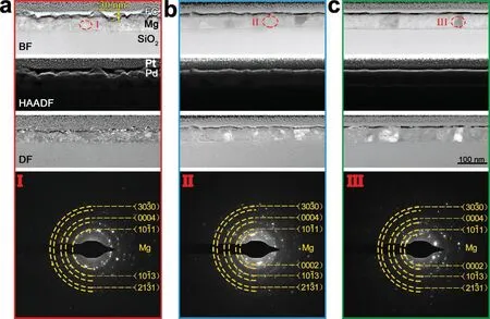
Fig.3.The cross-section structure and micro-diffraction pattern of FC/Pd/Mg films: BF,HAADF and DF images of the films with Mg deposited at (a) 40 W,(b) 150 W and (c) 300 W;microdiffraction pattern images corresponding to the positions marked I,II and III in BF images.
From the BF and DF images in Fig.3a,Mg (40 W) layer contains lots of nanograins.As sputtering power increases to 150 W,the size of grains enlarges.When the sputtering power reaches 300 W,column-like regions appear.Structure will have an influence on its morphology,column-like structure are typical during deposition which usually have hexagonal-like morphologies [27].This is consistent with the morphologies results (Fig.1f).
The micro-diffraction images of Mg layer indicate that the deposited Mg films are polycrystalline and exhibit a hexagonal structure.Most spots come from Mg,which means that there is no mixing between Pd layer and Mg layer.This is different from some studies which show that Mg grain is surrounded by Pd [28] or alloying effect between Mg and Pd[29],which may be caused by high temperature.
The microstructure of the films is analyzed in detail(Fig.4).Mg(40 W)layer consists of nano-sized grains,which is smaller than 10 nm in diameter.Grains in the film fabricated at 150 W have enlarged size (Fig.4b).When sputtering power reaches 300 W,Mg has some column-like regions with lots of dislocations inside.This region is shown typically with a highly preferential [0001] orientation along its growth direction as indicates by high resolution transmission electron microscope (HRTEM) and the fast Fourier transform (FFT)analysis.A corresponding schematic diagram is displayed in Fig.4d–4f.This evolution from nanosize to bigger-size grains after enlarging sputtering power is accordant with some studies[25].When the sputtering power increases,atoms get more energy leading to fast moving speed and generates high collision temperature,herein nucleation of Mg grains increases.However,when energy accumulates,Mg grains keep growing.Finally,some regions with big grains appear.With the further increase of sputtering power,column-like regions enlarge in sizes and numbers.
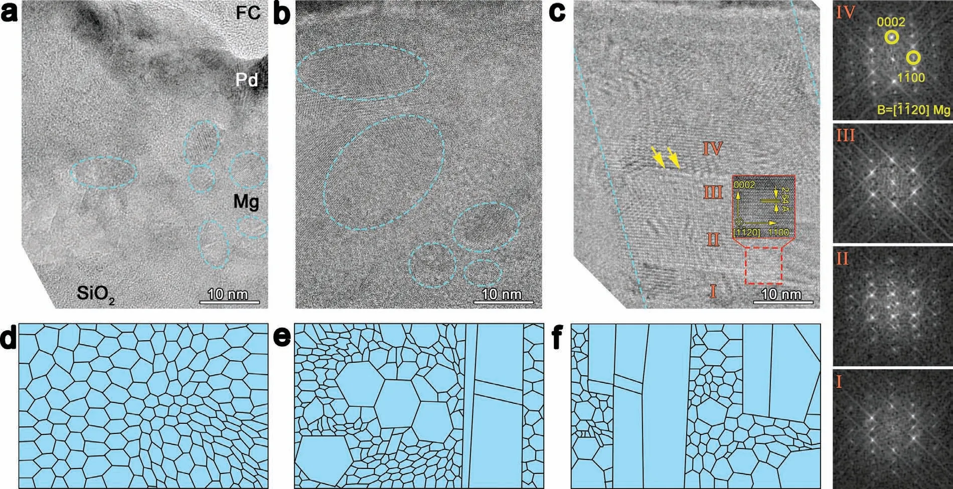
Fig.4.The cross-section microstructure images and the schematic illustrations of FC/Pd/Mg films with Mg layer fabricated: (a,d) at 40,(b,e) at 150 (c,f) and at 300 W;the inset shows HRTEM image in the square region and the arrow indicates the position of dislocations in (c);the FFT images are corresponding to I,II,III and IV marked in (c).
Herein,the internal structure of Mg layer has undergone significant changes under the influence of the sputtering power.This is consistent with the change tendency of its surface topography.Thus,Mg layers with different grain sizes in FC/Pd/Mg films have been successfully prepared.To study the role of grain size of Mg in hydrogenation/dehydrogenation thoroughly,further explorations on hydrogenation properties are performed using these films.
3.3. Hydrogen-induced optical properties of FC/Pd/Mg film
3.3.1.Reflectanceconversionrange
The hydrogenation properties of FC/Pd/Mg film were measured (Fig.5).From Fig.5a,Mg films fabricated at different sputtering powers have almost the same reflectance in reflective state,excepting the reflectance of FC/Pd/Mg (40 W) film is lowest.This is because the optical properties of metals are strongly related to their interface morphology [30,31].The rougher the surface of this film,the lower the reflectance.Furthermore,with the increase of the sputtering power,the reflectance of the FC/Pd/Mg film at transparent state is larger or the reflectance conversion range of the FC/Pd/Mg film becomes smaller.The reflectance conversion range of the FC/Pd/Mg (40 W) film is 68.1%,which is larger than values reported[32,33].On the contrary,the FC/Pd/Mg(300 W)film deposited has the narrowest reflectance conversion range of 19.5%.The hydrogenation of Mg involves the transformation from metal to MgH2semiconductor.This process is mainly affected by the internal structure of Mg films,as nanograins with smaller diameters often tends to have faster hydrogen sorption kinetics [10].Thus,this phase transformation related to structure might contribute to the different reflectance of the films in their hydrogenated state.
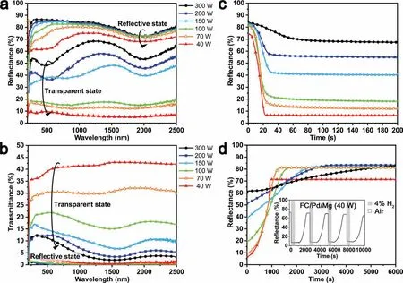
Fig.5.Typical optical properties measurements of FC/Pd/Mg films with Mg layer deposited at different sputtering powers: (a) reflectance spectra and (b)transmittance spectra at different wavelength ranges;(c) hydrogenation and (d) dehydrogenation properties at the wavelength of 980 nm;the inset image shows the cycle durability of FC/Pd/Mg (40 W).
3.3.2.Transmittanceconversionrange
The transmittance change of FC/Pd/Mg film is also depicted (Fig.5b).With the increase of the sputtering power of Mg layer,the transmittance conversion range of FC/Pd/Mg film shortens from 40.5% to 4.7%.The transmittance optical value 40.5% of FC/Pd/Mg (40 W) film is similar as reported[19].This means the FC/Pd/Mg (40 W) film absorbs hydrogen almost completely.
According to the Lambert-Beer law,the optical transmittance is proportional to thickness of films and hydrogen content inside films [34,35].The thickness of all the FC/Pd/Mg films prepared is almost the same in this study.Herein,changes in optical transmittance conversion range are mostly resulted from different hydrogen content ratios in Mg layer.During hydrogenation,Mg (Band gap,Eg=0 eV) transformed into dense hydride MgH2(Eg=5.6 ± 0.1 eV) layer,which will hinder the further diffusion of hydrogen atoms[19].If the size of Mg grains is too large,it can hardly hydrogenate completely [36,37].On the other hand,with the increase of the sputtering power,the grain size in Mg layer increases,leading to increasingly poor hydrogenation abilities.Thus,the optical transmittance conversion range of films changes because less amount of Mg (300 W) converts into transparent MgH2semiconductor.This also accounts for the high reflectance of FC/Pd/Mg (300 W) film at transparent state.
3.3.3.Hydrogenationanddehydrogenationprocess
The hydrogenation kinetics of FC/Pd/Mg film is shown in Fig.5c.The time when reflectance process begin until the reflectance conversion range increases/decreases to 90%is defined as dehydrogenation/hydrogenation rate [38].With the increase of the sputtering power of Mg layer,the time needed for FC/Pd/Mg film to reach saturated state prolonged.FC/Pd/Mg (40 W) film can hydrogen fully in 20 s,while FC/Pd/Mg (300 W) film needs 80 s.As shown in Fig.4,the interface between the Pd layer and the Mg layer is distinct.Thus,it is difficult to explain its hydrogenation properties by interface alloy theory [29].Thus,another aspect to explain this different kinetics property can be structure difference.Firstly,Mg (40 W) is nanostructured and contains more grain boundaries,while the Mg (300 W) film contains large columnar-like regions with more internal dislocations(Fig.4c) and less grain boundaries.Generally,compared to the crystal region inside grains,both grain boundaries and dislocations can serve as fast diffusion channels for hydrogen atoms [19,39,40].Increasing their amount can promote hydrogenation and dehydrogenation kinetics of Mg film [10,37].Besides,more Mg grains grow parallel to [0001] preferential orientation in 150 W and 300 W than at 40 W.As hydrogen atoms have to overcome more energy barrier when penetrating through closed-packing plane [22],herein the packing plane suppresses the diffusion of hydrogen atom.
The dehydrogenation kinetics of the film is similar with that of hydrogenation kinetics.As the sputtering power increases,the time required for film to completely dehydrogenate increases.Mg (40 W) film requires 908 s for complete dehydrogenation and Mg (300 W) needs 5060 s.The process of dehydrogenation is mainly accompanied by the nucleation and growth of Mg[41].Due to the large internal grain boundary populations,Mg (40 W) film can provide more nucleation sites,promoting the dehydrogenation reaction.Besides,the inset image in Fig.5d shows the properties of FC/Pd/Mg(40 W) film after four hydrogen loading/unloading process,which is meaningful because such cyclic hydrogenation performance of Pd/Mg thin films is outstanding in the existing studies.The reflectance range decreases relatively little from 68.1% to 60.0%.As nanostructured grains can promote cycle durability greatly [23,42–44],mass grain boundary population in FC/Pd/Mg (40 W) film can mediate its plasticity.Thus,the cyclic performance of FC/Pd/Mg thin films might be improved when Mg grains are finer.
According to the above discussion,the grain size might determine the hydrogen content ratio in Mg layer,while grain boundary population might have an impact on hydrogenation kinetics.However,this conclusion can hardly be reached distinctly only by the discussion above.The relationship between the hydrogen content ratio in the film and its corresponding structural changes should be analyzed further.
3.4. Structure of FC/Pd/Mg films after loading/unloading process
The difference in structures will lead to different degrees of hydrogenation.These films might have huge structural difference after hydrogen loading and unloading process which can facilitate subsequent analysis.FC/Pd/Mg (40 W) and FC/Pd/Mg (300 W) films are selected as objectives,considering their initial structures differs the most.The structures of FC/Pd/Mg (40 W) and FC/Pd/Mg (300 W) films after 50 cycles are analyzed.Based on the hydrogenation and dehydrogenation kinetics (Fig.5) and considering the degraded structure [45] of FC/Pd/Mg films prone to be oxidation,the experimental parameters for subsequent cyclic experiments were set as below: each switching cycle is conducted by exposing films to 4% H2in Ar (3 min,200 sccm) and subsequent air(15 min,300 sccm),before the experiment,the chamber is pre-flushed with Ar (1 min).
The structure of the FC/Pd/Mg (40 W) film after 50 cycles is displayed in Fig.6.The Pd layer is completely broken and the layered structure disappears (Fig.6a).According to the energy disperse spectroscopy (EDS) mapping images,Pd layer broken into nanocrystals and was mixed with the FC layer (Fig.6e,6f),while the Mg layer is composed of fine nano-sized grains (Fig.6b–6d).Thus,the expansion ruptures both Pd and Mg layer,which is consistent with previous reports [44].
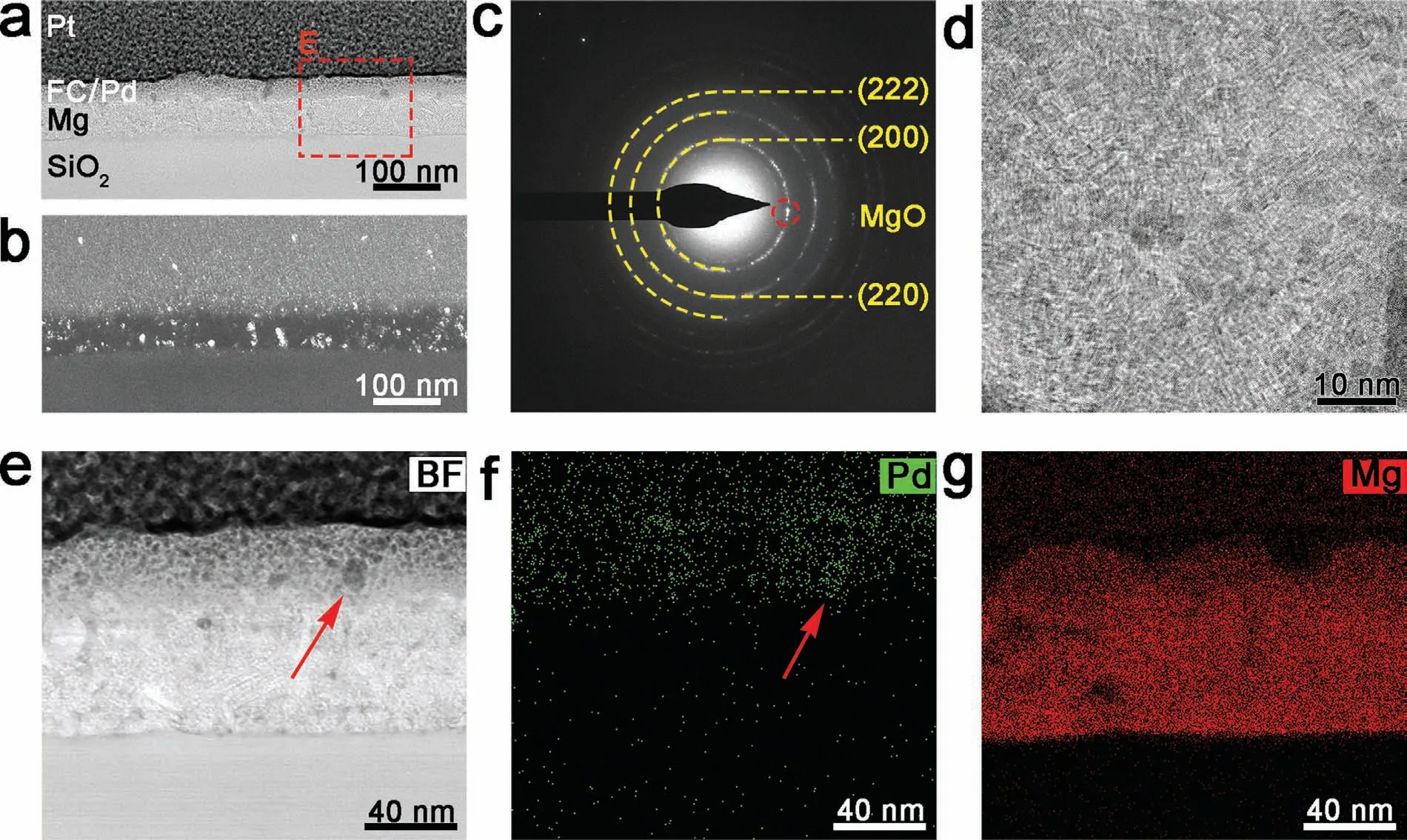
Fig.6.The cross-section structure of the FC/Pd/Mg (40 W) film after 50 hydrogen loading and unloading cycles: (a) BF image;(b) DF image taken from spots marked in (c) the microdiffraction pattern of the Mg layer;(d) HRTEM image of Mg layer.(e–g) BF and EDS images of region E in (a).
The structure of the FC/Pd/Mg (300 W) film after 50 cycles is shown in Fig.7.The Pd layer fluctuates greatly and becomes discontinuous (Fig.7a).Besides,the columnar-like area inside the Mg layer completely disappears,leaving only fine nanocrystals (Fig.7b–7e).This is consistent with the nanomodification of Mg from column-like crystal to nanostructure crystal reported before [27,46].Besides,the EDS results display that the interface between the Mg and the Pd layer is distinct (Fig.7f–7g).
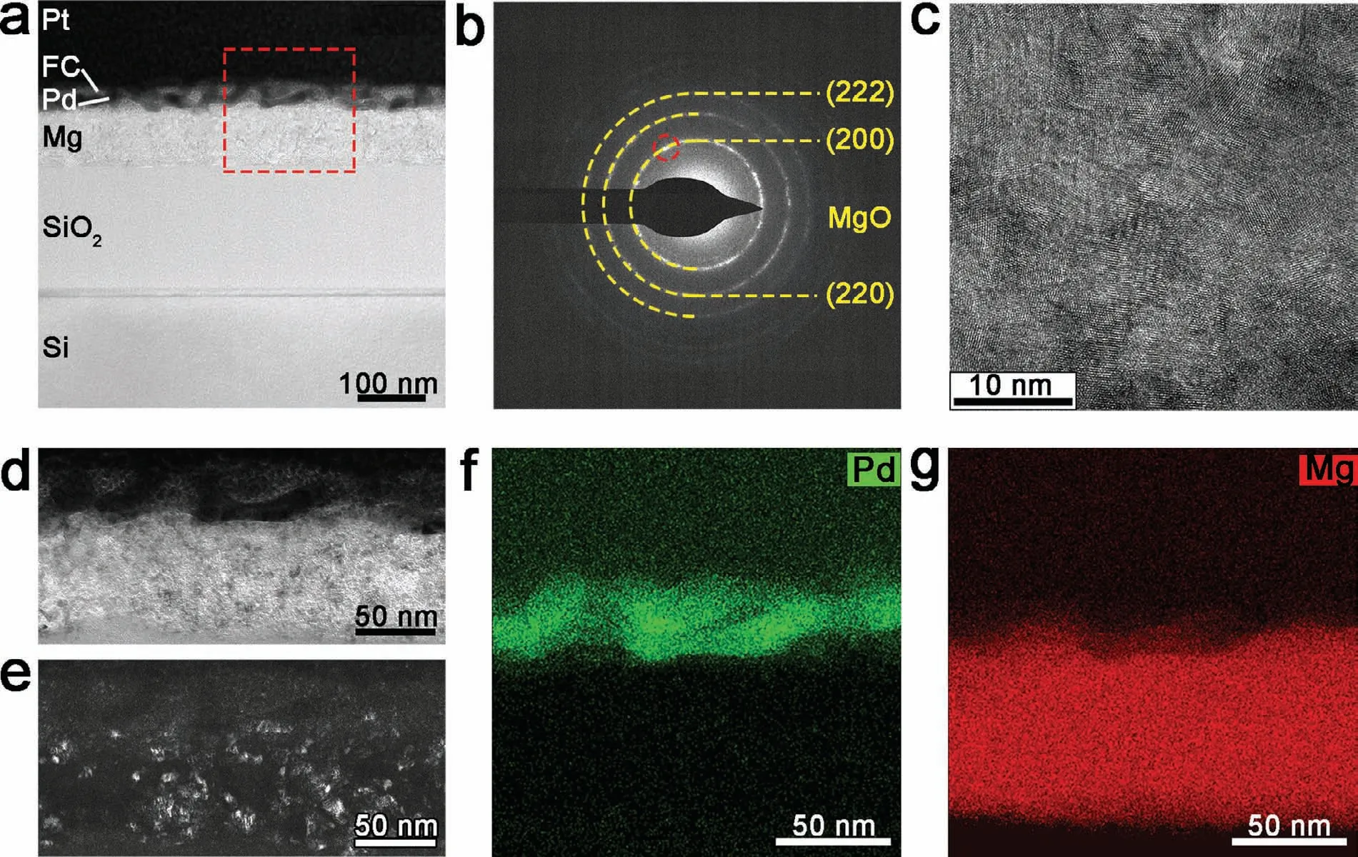
Fig.7.The cross-section structure of the FC/Pd/Mg (300 W) film after 50 hydrogen loading and unloading cycles: (a) TEM image;(b) the microdiffraction pattern and (c) HRTEM image of Mg layer;(d) BF,(e) DF is taken from spots marked in (c);(f,g) EDS images of region marked in (a).
When hydride is formed,phase transition leads to structure transformation which causes mass strain inside films.During the hydrogenation process,the volume change of Mg layer is greater than Pd layer [47].Besides,the greater tensile stress from the interaction with Mg layer rather than its own expansion inside Pd layer [48] causes the fracture of Pd layer.To some extent,the broken level of Pd layer in Pd/Mg film can illustrate the hydrogen content absorbed in Mg layer.Thus,severely breaking of the Pd layer in the FC/Pd/Mg (40 W)film after 50 cycles indicates the greater volume change in its Mg layer and a larger amount of hydrogen is absorbed in the Mg (40 W) layer.Besides,the cracking of the protective and catalytic Pd layer [27] leads the oxidation of Mg to MgO (Fig.6c),which suppresses the diffusion of hydrogen atoms [49] at room temperature.All of these contribute to the poor hydrogenation of the film after multiple cyclic experiments.However,nanostructure mediates plasticity by grain boundaries [23,42–44].Therefore,although the hydrogen content absorbed in FC/Pd/Mg (40 W) film is large,the nanostructure can still protect its durability in a few cycles(Fig.5d).However,only this result can still hardly explain the hydrogenation kinetics difference between FC/Pd/Mg films.
For one thing,the former structure observation experiment proves that Mg films will be refined into nanocrystals after hydrogenation [27].For another,large unreacted area can be observed after a hydride/dehydride cyclic process in initial columnar-like regions.Based on this,FC/Pd/Mg(300 W)film with mass column-like structures is ideal for a more detailed structural observation,to explain the different hydrogenation kinetics.
The structure of the FC/Pd/Mg (300 W) film after a hydride-dehydride cyclic process with a sufficiently long time is presented (Fig.8).This process is conducted by exposing films to 4% H2in Ar and subsequent air.Compared with its initial state (Fig.3c),the fluctuation of the Pd layer is slight (Fig.8a).The columnar-like regions that penetrate the entire film have disappeared in the Mg layer after hydrogenation.Instead,a typical crystalline region can be seen,which is composed of polycrystals (Fig.8b–8d).Fig.8e–8g images are the HRTEM schematic diagrams of these typical polycrystals.The experimental results show that this crystalline region can be divided into two parts with different structures.The upper part that close to the Pd layer contains many small nanosized grains,which are consist of regions like half-spheres[50].Generally,nanocrystals formed during sputtering process are close to the substrate,thus this nano-sized grain are supposed to generate be caused by structural nanomodification after hydrogenation (Fig.7).The other part close to the base is a big crystal with many defects inside (Fig.8g),of which the size and shape are similar to the column-like regions (Fig.3c).Thus,this crystal is likely to be the unreacted area of columnar-like grains.In addition,the grain boundary morphology(Fig.8e)between different crystalline regions has inapparent structural changes,which means that the grain boundaries are intact or still in its deposited state without hydrogenation.Besides,compared with the crystal region inside grains,the diffusion of hydrogen atoms along grain boundaries in the FC/Pd/Mg (300 W) films is even sluggish.

Fig.8.The cross-section structure of the FC/Pd/Mg (300 W) film after a hydride-dehydride cycle process with a sufficiently long hold time.(a) TEM image;(b) the microdiffraction pattern;(c) BF image of region marked in (a);(d) DF is taken from spot marked in (b);(e-f) HRTEM images of regions marked (c).
The effect of grain boundaries on the diffusion of hydrogen atoms might be related to its grain boundary energy.As for the FC/Pd/Mg (300 W) film,higher sputtering power leads to faster movement of atoms and higher temperature rise inside the film [51].Thus,the size of the internal Mg grains will be larger and the grain boundary population will be smaller.The temperature rise caused by atom collusion will bring a low grain boundary energy [52,53] of grains in Mg (300 W) film.Grain boundary with high energy often improve the diffusion of hydrogen atoms [44].On contrary,grain boundary with lower energy often traps hydrogen atoms,decreasing hydrogen atoms diffusion [40,54].This accounts for the slower hydrogenation properties of FC/Pd/Mg(300 W)film.In contrast,Mg layer in FC/Pd/Mg (40 W) film is a fine nanocrystalline structure with many randomly-distributed grain boundaries.These grain boundaries might have high energy,resulting in its faster hydrogen atoms diffusion speed.
4.Conclusions
In conclusion,to study the relationship between the structure and hydrogen-induced optical performance of the FC/Pd/Mg films,the internal structure of FC/Pd/Mg films were observed before and after cyclic hydrogen loading/unloading process.Mg film was tuned by adjusting the magnetron sputtering powers to slow the speed of sputtered atoms.The FC/Pd/Mg (40 W) film had the fastest hydrogenation/dehydrogenation kinetics that absorbed hydrogen in 20 s and desorbed in 908 s.This is due to its large grain boundary populations with high energy,which provided fast diffusion channels for hydrogen atoms in Mg (40 W) layer.Besides,this grain boundary can serve as nucleation sites to promote its dehydrogenation reaction.The FC/Pd/Mg (40 W)film with nanostructured Mg layer can hydride almost completely with the largest optical reflectance and transmittance conversion range of 68.1% and 40.5%,respectively.As the sputtering power is gradually increased from 40 to 300 W,the kinetic energy of the sputtered Mg atoms increased,allowing the atoms to move freely and the temperature inside the film increased,bringing lower grain boundary energy.This contributes to the slower rate of hydrogenation along grain boundaries than within grains,as evidenced by the structural observation of the FC/Pd/Mg (300 W) film after a long-enough-holding hydride-dehydride process.FC/Pd/Mg(300 W) film had more columnar-like crystal regions inside.All this leads to its slower hydrogenation kinetics rate prolonged by almost 4-and 5-fold compared with FC/Pd/Mg(40 W) film.Besides,the ratio of optical reflectance and transmittance conversion range reduced by 71.4% and 88.4%,separately.Thus,we had experimentally shown the possibility to tailor the thermodynamics of Mg-based films by means of tuning the grain boundary energy and grain size for the first time.This had reference values to the preparation of Mg-based hydrogen storage materials or hydrogen-induced gasochromic materials.In addition,this would be useful hints for understanding the diffusion behaviors of hydrogen atoms in other metals.Comprehensive studies are on-going to elucidate the influence of crystal size and grain boundary on the hydrogenation properties of FC/Pd/Mg films.
Acknowledgment
The authors greatly acknowledge the financial support from the National Key Research and Development Program of China (No.2016YFB0301001),Natural Science Foundation of Shanghai (No.20ZR1425000),Funding of Center of Hydrogen Science (WF510105001) and Open Fund of Key Lab Superlight Materials and Surface Technology,Ministry of Education.The authors also appreciate experimental support from the Instrument Analysis Center.We want to thank for the support from Center for Advanced Electronic Materials and Devices (SJTU).We are also thankful to Prof.Hong Wang and Dr.Cai Chen for their kind assistances.
Conflic of interest
The authors declare no competing financial interest.
 Journal of Magnesium and Alloys2023年6期
- Journal of Magnesium and Alloys的其它文章
- Ameliorating the re/dehydrogenation behaviour of MgH2 by zinc titanate addition
- Inhibiting effect of I-phase formation on the plastic instability of the duplex structured Mg-8Li-6Zn-1.2Y (in wt.%) alloy
- PEO coating on Mg-Ag alloy: The incorporation and release of Ag species
- Underlying mechanisms of variation in yield asymmetry and strain hardening behavior of extruded pure Mg with Gd addition
- Edge crack damage analysis of AZ31 magnesium alloy hot-rolled plate improved by vertical roll pre-rolling
- High sintering and dielectric performance: The improved (Mg,Zn)3B2O6 ceramics with the help of the DFT calculation
