
Growth behaviors and emission properties of Co-deposited MAPbI3 ultrathin films on MoS2
2023-02-20 13:16:24SiwenYou游思雯ZiyiShao邵子依XiaoGuo郭晓JunjieJiang蒋俊杰JinxinLiu刘金鑫KaiWang王凯MingjunLi李明君FangpingOuyang欧阳方平ChuyunDeng邓楚芸FeiSong宋飞JiataoSun孙家涛andHanHuang黄寒
Chinese Physics B 2023年1期
Siwen You(游思雯), Ziyi Shao(邵子依), Xiao Guo(郭晓), Junjie Jiang(蒋俊杰), Jinxin Liu(刘金鑫),Kai Wang(王凯), Mingjun Li(李明君), Fangping Ouyang(欧阳方平), Chuyun Deng(邓楚芸),Fei Song(宋飞), Jiatao Sun(孙家涛), and Han Huang(黄寒),†
1Hunan Key Laboratory of Super-Microstructure and Ultrafast Process,School of Physics and Electronics,Central South University,Changsha 410083,China
2College of Arts and Science,National University of Defense Technology,Changsha 410073,China
3Key Laboratory of Interfacial Physics and Technology,Shanghai Institute of Applied Physics,Chinese Academy of Sciences,Shanghai 201000,China
4School of Information and Electronics,MIIT Key Laboratory for Low-Dimensional Quantum Structure and Devices,Beijing Institute of Technology,Beijing 100081,China
Keywords: MAPbI3/MoS2 heterostructure, Co-deposition, temperature-dependent photoluminescence,growth behavior
1. Introduction
Perovskites (PVKs) have raised much attention in semiconductor applications, such as solar cells, light emitting diodes,and photodetectors,due to their exceptional optoelectronic properties.[1–5]Among them, MAPbI3is a representative one due to its simple structure,suitable bandgap for solar absorption, and long-range balanced electron–hole transport lengths.[6,7]Properties of elementary excitation of MAPbI3,such as the values of exciton binding energy and the strength of electron-phonon coupling,are essential for development of high-efficiency devices. According to the temperature dependence of integrated intensity of the photoluminescence (PL)emission peak, the exciton binding energy of MAPbI3has been extracted to be 15–60 meV,[8–10]which is so small that separation and migration of electrons and holes in MAPbI3thin films(300 nm)can be facilitated. Electron–phonon coupling sets a basic intrinsic limit to charge carrier mobility in non-intrinsic scattering without impurities and has been proved to generate homogeneous emission linewidth broadening in semiconductors.[11]Especially,it has comparable effects on temperature-induced renormalization of bandgap with thermal expansion in MAPbI3bulk or thin films, but enhanced contribution in MAPbI3nanocrystals in size of several nanometers because of the strong quantum confinement effects.[12]
Accompanied with the miniaturization of devices, the functional material films become thinner and thinner.MAPbI3thin films prepared by the solution spin coating method are usually several hundreds of nm in thickness and their properties are close to their bulk counterparts.[13]Methylammonium lead tribromide nanocrystals in different sizes (1.5–3 nm)formed in metal oxide porous scaffolds show a wavelengthtunable emission from green to blue due to the quantum confinement effects.[14]Highquality MAPbI3nanosheets as thin as 1.3 nm have been fabricated by converting solutionprocessed PbI2in MAI vapor, but the preparation process and their thicknesses are not controllable.[15]Transition-metal dichalcogenides (TMDCs) are good templates to realize van der Waals epitaxial growth of MAPbI3due to the dangling bond-free surfaces.[16–19]In previous reports,thicknesscontrollable MAPbI3ultrathin layers are successfully fabricated on chemical vapor deposition(CVD)-grown or mechanical exfoliation monolayer TMDCs using a two-step sequential deposition method.[20,21]However, such a method has some shortcomings, such as the volume expansion and structure damage in MAI intercalation process. The Co-deposition method is superior for preparing MAPbI3thin films with a wide range of clean interfaces,homogeneous morphology,and better stability.[22–25]However, it is still of challenge to prepare and investigate properties of ultrathin MAPbI3thin films with high quality.
In this work, we systematically investigate the growth behaviors of MAPbI3films via co-deposition of PbI2and MAI on CVD-grown monolayer MoS2as well as the corresponding photoluminescence properties and emission behaviors at different growing stages using atomic force microscopy (AFM), scanning electron microscopy (SEM), PL,and Kelvin probe force microscopy (KPFM) measurements.Temperature-dependent PL measurements reveal thicknessdependent trends of emission photon energy in MAPbI3/MoS2heterostructures from 300 K to 80 K.
2. Experimental methods
Monolayer MoS2was prepared by the conventional CVD method with two temperature zone systems on the c-sapphire substrate. S (aladdin 99.999%) and MoO3(aladdin 99.99%)powders were used as precursors,as well as nitrogen(N2)carries the reactants as an inert gas.[26,27]A previously reported co-deposition method was adopted to fabricate MAPbI3ultrathin films on c-sapphire substrates partially covered with monolayer MoS2in a high-vacuum system with base pressure better than 5.0×10⁻⁵Pa.[22,28]There are two temperaturecontrolled K-cells at the bottom of the system, loaded with the precursor materials of PbI2(aldrich, 98+%) and MAI(polymer, 99.5%), respectively. The deposition temperatures of PbI2and MAI are 573 K and 415 K, respectively, and the deposition rates of the precursor at 6 ˚A/min for PbI2and 15 ˚A/min for MAI are monitored by quartz crystal microbalance. The deposition times are 2 min, 4 min, and 6 min.The corresponding samples with a nominal thickness~2 nm,4 nm,and 8 nm are named as samples I,II,and III,respectively.
AFM measurements were carried out in a tapping mode(Agilent 5500, USA).[29]SEM was obtained with an MIRA3 LMH(TESCAN Chech)field emission scanning electron microscope. PL spectra were collected in a confocal Raman microscope system(Renishaw inVia Qontor,UK)using a 532 nm laser and 1800 lines/mm grating,where a sample stage(THMS 600) with the temperature varying from 78 K to 873 K is equipped.[30,31]All spectra were taken at laser power density 1 mW/μm2for 1 s and were fitted by Gaussian and Lorentzian mixed deconvolution. X-ray diffraction(XRD)patterns were measured by a PANalytical Empyren system with CuKαradiation(λ=0.154 nm). KPFM images were recorded using an NTEGRA spectra system(NT-MDT,Russia).
3. Results and discussion
Figure 1(a) shows a typical AFM image of a triangular CVD-grown MoS2flake, whose thickness is~0.9 nm, as shown in the profile along the red line, indicating a monolayer MoS2.[32]Upon 2 nm MAPbI3deposition (sample I),dispersed bright protrusions with a height up to 8 nm appeared on the bare c-sapphire surface, as shown in Fig. 1(b). On the contrary,the MoS2flake appears as atomically smooth as the pristine one except for some features on its edges. The corresponding line profile displays that the thickness in the triangular MoS2region is almost doubled (~1.6 nm), and the dim features have an additional height of~0.8 nm, indicating that a monolayer MAPbI3is grown on MoS2, and new nuclei start at the edges. Upon 4-nm MAPbI3deposition (sample II), the bright protrusions on c-sapphire (region B)became denser and higher(~30 nm)as shown in Fig.1(c),indicating a nucleation-limited growth. The triangular MoS2region(region A)has no apparent change except that its thickness increases to 4 nm. We speculate that at the beginning,MAPbI3grows in a Frank–van der Merwe mode on MoS2and in a Volmer–Weber mode on c-sapphire. Different growth behaviors of MAPbI3on two substrates may be attributed to their different hydrophilicity and lower nucleation energy on MoS2.[16,33]Therefore, MoS2is a good template to realize van der Waals epitaxial growth of MAPbI3due to the dangling bondfree surface. Upon 8-nm MAPbI3deposition(sample III),although the triangular shape of MoS2is still observable, the entire surface is covered by clusters (up to 60 nm high) as shown in Fig. 1(d), indicating that the growth mode of MAPbI3on MoS2changes to the Stranski–Krastanov(S-K)mode. It reveals the limited influence of MoS2on the growth of MAPbI3. The SEM image in Fig. 1(e) shows the grainy features in more details than the AFM image due to no tip effect.The averaged grain size of MAPbI3on MoS2(~500 nm)is larger than that on the c-sapphire substrate(~200 nm)because the dangling-bond-free surface of MoS2could motivate the migration of atoms precursor molecules (MAI and PbI2)and promote the growth of MAPbI3grains,which is in agreement with the previous reports.[16,17]The corresponding XRD pattern in Fig.1(e)shows the peaks at 14.2°,28.3°,and 33.1°,assigned to the (110), (220), and (310) planes of crystalline MAPbI3in the tetragonal phase, respectively.[34]The grain dimension in the perpendicular direction is estimated to be~33 nm according to the Scherrer equation. No PbI2related peaks can be detected,confirming the high quality of the prepared sample. Figure 1(f) schematically demonstrates the growth modes of MAPbI3on MoS2. The x-ray photoelectron spectra(XPS)full spectra of samples are shown in Fig.S1 in the supporting information, where Pb, I, N, and C elements are detected. In the future, atomically resolved methods like high resolution transmission electron microscopy (HRTEM)and scanning tunneling microscopy(STM)can be used to investigate the detailed structure or the quality of MAPbI3/MoS2heterostructures.
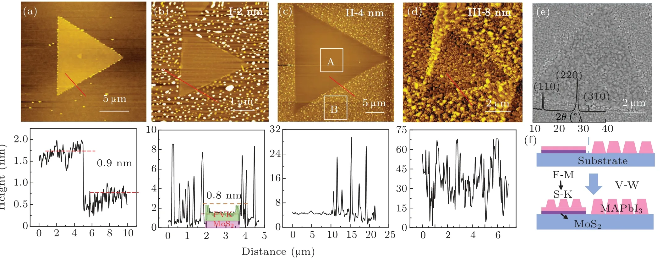
Fig.1. Typical AFM images of CVD-grown MoS2 on c-sapphire(a),and co-deposited MAPbI3 ultrathin films in various nominal thicknesses[(b)2 nm,(c) 4 nm, (d) 8 nm)] on top, named as sample I, II, and III. The corresponding scan profiles are given. (e) Representative SEM image of 8-nm-thick MAPbI3 (sample-III).The corresponding XRD pattern is inserted. (f)Schematic illustration of different growth modes of MAPbI3 on c-sapphire with and without MoS2.
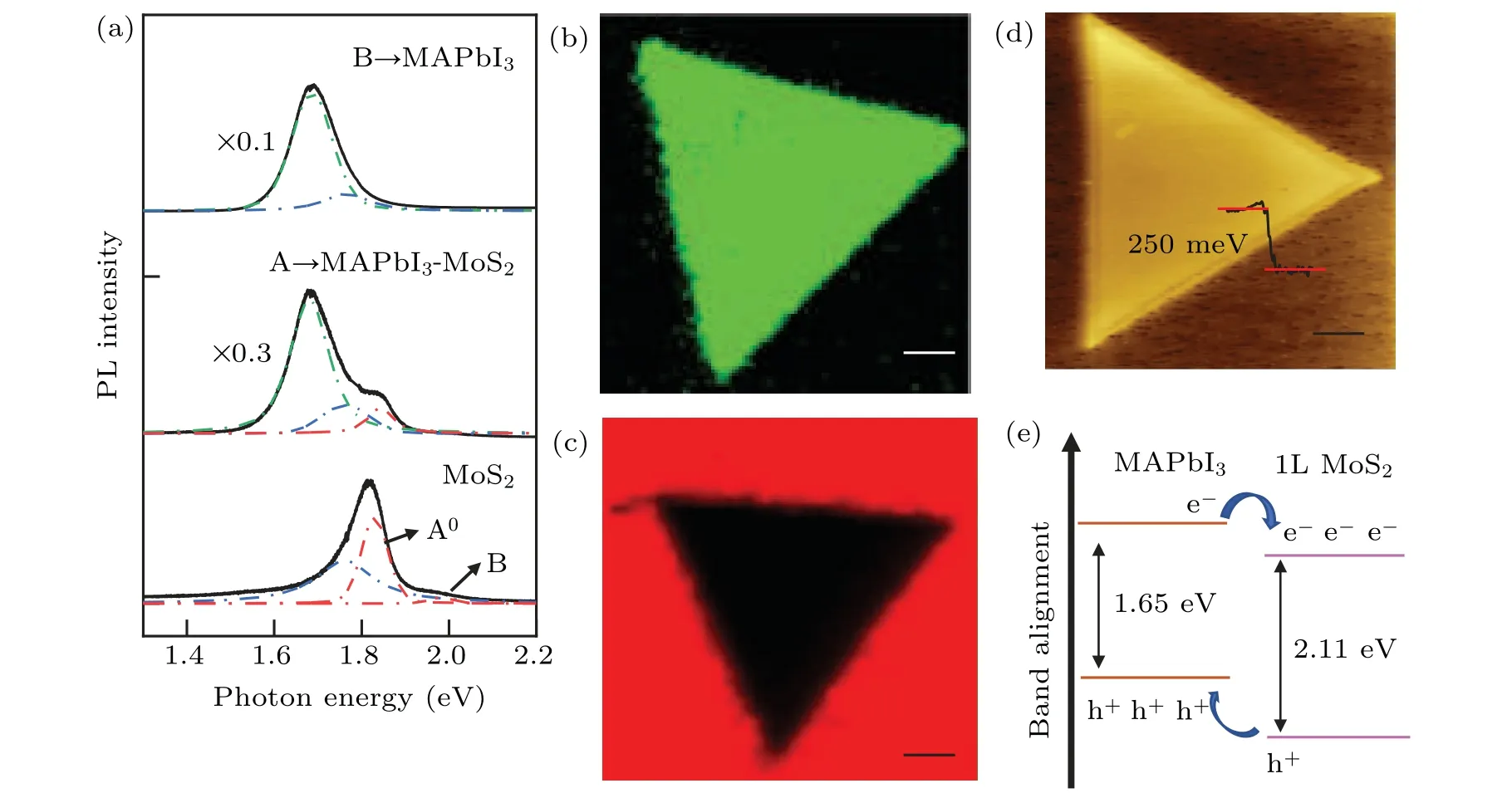
Fig.2.Characterizations of MAPbI3/MoS2 heterostructure(sample II):(a)PL spectra collected from CVD-grown MoS2,MAPbI3 on c-sapphire with and without MoS2 regions, (b) PL mapping of a CVD-grown MoS2 flake, (c) PL mapping and (d) KPFM image of the MAPbI3/MoS2 heterostructure. Scale bar: 5 μm. (e)Schematic illustration of the type-II energy level alignment of MAPbI3/MoS2 heterostructure.
PL measurements were performed to investigate the optical properties of sample II, as shown in Fig. 2(a). The peak intensities were normalized by the bottom panel. The PL spectrum of CVD-grown MoS2exhibits three peaks(fitted)at 1.76 eV,1.84 eV,and 1.99 eV,corresponding to the free exciton of c-sapphire substrate(blue plot), exciton A and exciton B of MoS2(red plot),respectively. The better distribution and uniformity of MoS2can be reflected by the PL mapping of exciton A,as shown in Fig.2(b). For sample II,two representative PL spectra from regions A and B are shown in Fig.2(a).Besides the original emission peaks of MoS2and sapphire,an additional emission peak centered at 1.68 eV with a full width at half maximum(FWHM)of 0.11 eV can be observed,which belongs to the MAPbI3(green plot). It is worth noting that the emission peak intensity of MoS2is higher than that of sapphire without MAPbI3,while they are almost equal after deposition of MAPbI3, revealing the quenching of MoS2emission peak intensity. Moreover,the PL intensity of MAPbI3on MoS2(region A)is quenched by a factor of 3 times compared to that on c-sapphire(region B).As shown in Fig.2(c),the PL intensity mapping at 1.68 eV was measured. It was observed that the PL intensity in region A was significantly lower than that in region B, indicating the PL quenching of MAPbI3on MoS2.For sample III, the PL emission peak of MAPbI3is located at 1.64 eV and there is no MoS2signal anymore because of strong luminescence properties of thicker MAPbI3, as shown in Fig. S2(a). The clear redshift of the emission peak can be ascribed to the thickness-dependent quantum confinement effect of MAPbI3layer.[20]Moreover,the intensity of emission peak is still quenched in the heterostructure.
To further investigate the surface charge distribution in heterostructures,KPFM measurements were carried out. The contact potential difference(CPD)is defined as the work function difference between the sample surface and the cantilever tip. As shown in Fig. 2(d), the CPD difference between MAPbI3/MoS2and pure MAPbI3regions is determined to be about 250 mV,which indicates that the work function of pure MAPbI3is 250 meV smaller than that of MAPbI3/MoS2. It reveals the formation of electric dipoles pointing out of the plane in the MAPbI3/MoS2heterostructure region,due to the interfacial electron transfer from MAPbI3into MoS2, resulting in separation of holes and electrons distributions on two sides.[18,35,36]Taking the PL quenching at the heterostructure interface into consideration, we can get a conclusion that a representative type-II band alignment of MAPbI3/MoS2heterostructure is formed as shown in Fig. 2(e), which is in agreement with the previous reports.[17,21,37,38]Taking the transport gaps of MAPbI3and monolayer MoS2as 1.65 eV and 2.11 eV,[39]respectively,both conduction band minimum(CBM)and valence band maximum(VBM)levels of MAPbI3are higher than those of MoS2.[40,41]For sample III, the CPD difference is~20 mV [see Fig. S2(b)], which may be attributed to the different morphologies of the heterostructures.The work function of MAPbI3changes as the surface becomes rougher. Profiting from the effective interfacial charge carrier separation in ultrathin type-II MAPbI3/MoS2heterostructure,they are excellent candidates for designing high-performance photodetector devices.
To better understand the thickness-dependent photophysical properties of MAPbI3/MoS2, temperature-dependent PL measurements from 300 K to 80 K are carried out. Figure 3(a) shows the temperature evolutions of PL spectra of sample III.There is a dominant and symmetric emission peak located at around 1.64 eV(peak I),belonging to the tetragonal-I phase (I4/mcmgroup) MAPbI3.[9]Below 150 K, a new emission peak appears at 1.69 eV (peak II), arising from the orthorhombic phase MAPbI3. These emission peaks of tetragonal and orthorhombic phase are ascribed to the free exciton recombination.[41]The atomic models of tetragonal and orthorhombic phases are shown in the insets of Fig. 3(a).[42]In order to understand the evolution of fitting emission peak,PL spectra at six representative temperatures are shown in Fig. S3. As the temperature decreases to 100 K, a newemerging emission component occurs at the low-energy side centered at 1.56 eV (peak III), which can be attributed to the trap-mediated exciton radiative recombination.[43]Figure 3(b)shows the photon energy evolution of the fitted three emission peaks of MAPbI3with temperature according to the experimental spectra. Peak I has a redshift from 1.64 eV to 1.59 eV in the temperature range from 300 K to 150 K. This trend is consistent with the previous report on pure MAPbI3.[9]The phase transition from tetragonal to orthorhombic for such MAPbI3/MoS2starts to take place at 150 K, which is higher than that for pure MAPbI3(~120 K),close to that of bulk.[12]From 150 K to 100 K, peak I (tetragonal) displays a slight blueshift while peak II(orthorhombic)keeps the trend of redshift. According to the integrated intensity of the fitted three emission peaks, the relative percentage evolution as a function of temperature is shown in Fig.3(c). As the temperature decreases, the ratio of the tetragonal phase goes down continuously while that of orthorhombic increases. It is worth noting that the ratio of trapped exciton peak keeps growing at low temperatures, attributed to the smaller binding energy of trapped excitons and surface state transitions.[41]
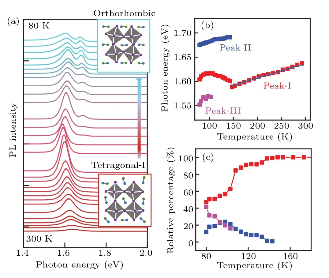
Fig.3. Optical transition properties of sample III in the temperature range of 300–80 K.(a)Temperature-dependent PL spectra. (b)Experimental data and fitting curve of photon energy as a function of temperature. Red: tetragonal phase. Blue: orthorhombic phase. Purple: the defect peak. (c)Relative percentage of three peaks in MAPbI3/MoS2 heterostructure.
For MAPbI3on MoS2in sample II (region A), the evolution of PL spectra as a function of temperature looks rather different, as shown in Fig. 4(a). The intensity of the main peak located at 1.68 eV (peak IV) increases as the temperature decreases from 300 K to 120 K. It results from the enhanced optical matrix elements on account of the reinforced Coulomb attraction, and is a representative behavior of freeexciton radiative recombination.[41]Although the PL signal of MoS2is weak,a blueshift of photon energy is still observable,consistent with the trend of traditional semiconductors.[44]See Fig.S4 for more details. No trapped exciton peak can be detected,suggesting less defect density in sample II.
Figure 4(b)displays the evolution of the extracted photon energy as a function of temperature.There is a turning point at 260 K for peak IV(red plot). Its photon energy exhibits a linear redshift from room temperature to 260 K,then a non-linear blue-shift from 26 K to 120 K. It is obviously different from that of sample III and previous results.[9,12,21]Below 120 K,a new peak appears at 1.72 eV (peak V, blue plot), which belongs to the orthorhombic phase MAPbI3. More details about the peak fitting are shown in Fig. S5. For comparison,temperature-dependent PL measurements were carried out on region B in sample II(black plot). The evolution of the main peak’s photon energy coincides with that in region A except for that in the range from 300 K to 260 K(peak VI).It is wellknown that the photon energy evolution as a function of temperature in either single crystalline bulk or thin films[45]keeps a linear redshift in the stable tetragonal phase and a secondorder phase transition from tetragonal to orthorhombic occurs at low temperature.[46]Moreover, MAPbI3nanocrystals with a size less than 8 nm have no apparent phase transition even at a temperature as low as 80 K.[12]Although MAPbI3on sapphire in sample II is nanocrystals, their sizes are significantly larger, close to those in the thin-film phase. The different photon energy evolutions in sample II may show a special crystal/electronic-structure relationship. A similar trend to that of MAPbI3on MoS2is observed in MAxFA1-xPbI3films accompanied by a different phase transition,[45]where a turning point in the photon energy evolution is attributed to the occurrence of a second-order transition from cubic to tetragonal phase. Here, MAPbI3was co-deposited on the monolayer MoS2and growing in van der Waals epitaxy, forming a clean and molecular sharp interface. We propose that MAPbI3in cubic phase may be formed at room temperature on MoS2and a second-order phase transition from cubic to another different tetragonal phase occurs at 260 K, called tetragonal-II.Below 120 K,a transition from tetragonal-II to the orthorhombic phase starts to take place. For MAPbI3on sapphire, one phase transition from tetragonal-II to orthorhombic starts to take place at 100 K. The atomic mode of tetragonal-II phase belonging to theI4cmspace group is shown in the inset of Fig. 4(a),[47]where the disordered organic cations may rotate in increments along thec-axis and affect the tilting of the corner-shared PbI6octahedron.Moreover,the tilting increases with the temperature decreasing. It gives rise to an opposite effect to the electron-phonon coupling induced gap renormalization, leading to the non-monotonic change of the photon energy.[48]
Figure 4(c)shows the evolution of the extracted FWHM of peak IV with temperature.The broadening behaviors can be described by the one-oscillator model of the electron–phonon interaction:[49]
Here,Γ0is the inhomogeneous broadening contribution depending on the crystal quality,which is a constant and does not change with temperature;σandΓopare the exciton-acoustic phonon interaction and the exciton-optical phonon contribution to the FWHM broadening; ¯hωopis the efficient opticalphonon energy, corresponding to the torsion mode of the organic cations.[45,50]Due to the main emission peak belonging to the free-exciton recombination,σ=0 is reasonable for ignoring the acoustic-phonon contribution.In the best fitting,the parameters areΓ0=30.0±2.3 meV,Γop=144.7±7.5 meV,and ¯hωop=25.1±5.0 meV, in agreement with the previous report.[21]Molecularly thin film of MAPbI3prepared by codeposition on monolayer MoS2has better crystalline and novel exciton behavior,which could be beneficial for getting atomically clean interfaces and investigating related properties.
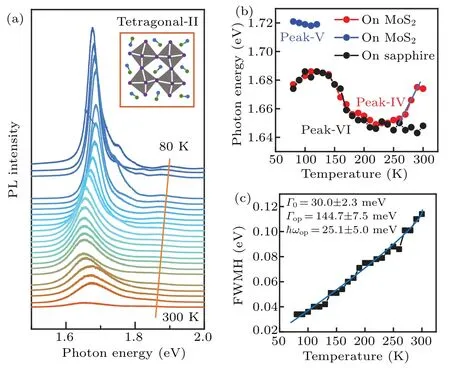
Fig.4. Optical transition properties of sample II in the temperature range of 300–80 K. (a) Temperature-dependent PL spectra. Inset: atomic model of tetragonal-II phase. (b) Experimental data of photon energy of MAPbI3/MoS2 (red: tetragonal phase,blue: orthorhombic phase)and pure MAPbI3 (black). (c) Experimental data (black) and fitting curve (blue) of FWHM of tetragonal phase as a function of temperature on MAPbI3/MoS2 heterostructure.
4. Conclusion
In summary, while MAPbI3grows in a Volmer–Weber mode on sapphire,it can appear in a Stranski–Krastanov mode on single layer MoS2, which gives an opportunity to prepare molecularly thin MAPbI3/MoS2heterojunction. Such heterojunctions have a type-II energy level alignment and are good candidates for optoelectronic devices.Temperature-dependent PL measurements reveal that such molecularly thin MAPbI3has a different emission property compared with thin films of either nanocrystals or bigger grains. The second-order phase transitions are observed at 120 K and 150 K.Our research creates more potential to fabricate molecularly thin heterostructures and provides a platform to study novel applications.
Acknowledgements
Project supported by the National Natural Science Foundation of China(Grant Nos.11874427 and 11804395)and the Fundamental Research Funds for the Central Universities of Central South University(Grant No.2020zzts377).
猜你喜欢
作文小学中年级(2021年12期)2022-01-21 03:19:52
湖北理工学院学报(人文社会科学版)(2020年4期)2020-07-24 02:52:58
传奇·传记文学选刊(2020年6期)2020-06-29 07:42:27
智富时代(2019年2期)2019-04-18 07:44:42
作文周刊·小学一年级版(2016年4期)2016-08-11 12:58:13
意林绘阅读(2016年2期)2016-03-09 07:23:24
金色年华(2016年2期)2016-02-28 01:38:42
高中生学习·高三版(2015年2期)2016-01-04 22:41:24
小小说月刊(2014年8期)2014-08-29 03:36:08
小品文选刊(2014年16期)2014-05-08 04:58:20
- Chinese Physics B的其它文章
- LAMOST medium-resolution spectroscopic survey of binarity and exotic star(LAMOST-MRS-B):Observation strategy and target selection
- Vertex centrality of complex networks based on joint nonnegative matrix factorization and graph embedding
- A novel lattice model integrating the cooperative deviation of density and optimal flux under V2X environment
- Effect of a static pedestrian as an exit obstacle on evacuation
- Chiral lateral optical force near plasmonic ring induced by Laguerre–Gaussian beam
- Adsorption dynamics of double-stranded DNA on a graphene oxide surface with both large unoxidized and oxidized regions