
Engineering large-scaled electrochromic semiconductor films as reproductive SERS substrates for operando investigation at the solid/liquid interfaces
2023-01-30 06:49LinglingYngJiujuFngJiNingWngZhidGoJingwnXuMiYnYnSong
Chinese Chemical Letters 2022年12期
Lingling Yng ,Jiuju Fng ,Ji-Ning Wng ,Zhid Go ,Jingwn Xu,*,Y Mi ,c,d,*,Yn-Yn Song ,*
a College of Sciences,Northeastern University,Shenyang 11000 4,China
b State Key Laboratory of Precision Spectroscopy,School of Physics and Electronic Science,East China Normal University,Shanghai 200062,China
c NYU-ECNU Center fo r Computational Chemistry at NYU Shanghai,Shanghai 20 0062,China
d Collaborative Innovation Center of Extreme Optics,Shanxi University,Taiyuan 030006,China
e College of Chemistry and Life Sciences,Zhejiang Normal University,Jinhua 3210 0 4,China
Keywords:Charge transfer Electrochromism Oxygen vacancies SERS substrate Solid/liquid interface
ABSTRACT Although surface-enhanced Raman spectroscopy(SERS)has been applied for gathering fingerprint information,even in single molecule analysis,the decayed Raman signals in aqueous solutions largely obstruct the on-site insight reaction process.In this study,large-scaled semiconductor films with multiwalled(TiO2/WO3/TiO2)nanopore distribution are fabricated by combining electrochemical anodization and sputtering technique,and then employed as the SERS substrates for detection of molecules at the solid/liquid interfaces.Given the remarkably improved electrochromic property of the multi-walled film,such SERS substrates were endowed with tunable oxygen vacancy(VO)density and distribution via simply applying electrochemical bias voltage,which enabled one to achieve an enhanced charge transfer efficiency and thus a remarkably increased Raman signal even in solution.The VO-rich SERS substrate is highly repeatable,thus providing a reliable platform for in-situ monitoring of the target molecules or intermediates at the solid/liquid interfaces.
Titanium oxide(TiO2),known by its high stability and electronic properties,constitutes a versatile platform in the fields of photocatalysis,energy storage,and biomedical applications[1–3].Operando monitoring of the reactions on a TiO2surface is extremely important for investigating the yields of TiO2-based photocatalysts.The full understanding of the reactions at the water/TiO2interface is crucial for further optimization of TiO2based photocatalysts or reactors[4].However,in-situmonitoring of the reactions on the TiO2surface,especially on-site reactions,under operando conditions is still a challenge.In that regard,surfaceenhanced Raman spectroscopy(SERS)is an ideal analytical technology for ultrasensitive surface chemical analysis[5–8].For example,SERS was successfully employed by Tianet al.to investigate the photoinduced reaction on the solid/gas interface of singlecrystal TiO2[9].As a matter of fact,most common TiO2-based catalysts are generally low-cost polycrystalline composites and TiO2nanomaterials are usually applied in a liquid environment.Meanwhile,compared with strong signals from a solid/gas interface,the largely decayed Raman signals in the liquid medium mean that the use of semiconductor-based SERS substrates in practice is diffi-cult[10].Therefore,improving the SERS activity of semiconductorbased substrate in liquid medium has become an urgent task.
For semiconductor-based SERS substrates,it is generally agreed that the tuning of photoinduced charge-transfer(PICT)through band energy alignment between substrate and molecule plays a dominant role[11].Till now,lots of strategies have been developed to promote PICT efficiencies,such as n-/p-doping and stoichiometry[12–14].Especially,injecting oxygen vacancies(VO)as an important method in stoichiometry has been demonstrated to be useful for providing some additional defect levels in the bandgap of semiconductors,thus facilitating the exciton resonance in semiconductors,as well as the charge transfer(CT)between semiconductors and molecules[15–17].Recently,the SERS activities of selforganized TiO2nanotubes have been discovered by Weidinger and coworkers[18].Nevertheless,the Raman activity of TiO2nanotube arrays is significantly inferior to that of layered two-dimensional(2D)semiconductor materials,which have been demonstrated to possess a large number of structural defects[19–21].Besides the structural defects induced VO,Zhao and coworkers also utilized electrochromic technology to introduce VOinto the WO3substrate[22].Inspired by the intrinsic electrochromic capacity,feasibility,and widespread applicability of TiO2nanopore films(TiO2NPs)prepared by electrochemical anodization[23,24],we hypothesis that VOwould be also inserted by an electrochromic way,thus enabling TiO2NPs to be employed as alternative SERS substrates.
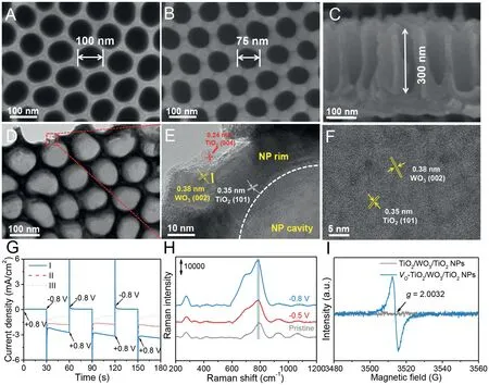
Fig.1.SEM images of(A)TiO2 NPs and(B,C)TiO2/WO3/TiO2NPs.(D)TEM,HAADF-STEM(inset),and(E,F)HR-TEM images of TiO2/WO3/TiO2NPs.(G)Current density vs.time curves of Ti O2 NPs(I),TiO2/TiO2NPs(II),and TiO2/WO3/TiO2 NPs(III)acquired during potential pulse cycling in a voltage range from–0.8 V to+0.8 V.(H)SERS spectra of TiO2/WO3/TiO2NPs after applying different bias voltage.(I)EPR spectra of TiO2/WO3/TiO2NPs and VO-TiO2/WO3/TiO2NPs.
For this purpose,we developed a facial and effective approach to prepare a large-scale porous semiconductor substrate with good electrochromic performance.The SERS measurements were carried out by employing bis(tetrabutylammonium)dihydrogen bis(isothi ocyanate)bis(2,2′-bipyridyl-4,4′-dicarboxylate)ruthenium(II)(N719)placed onto TiO2/WO3/TiO2NPs.The generation of tunable VOviaelectrochromic processing of the substrate resulted in the noticeable increase of the Raman signals of N719,and the PICT-mediated signal enhancement was attributed to the VOinduced by electrochromic effect.
The multi-walled NPs were constructed on the self-ordered TiO2NPs that were prepared by electrochemical anodization.The scanning electron microscopy(SEM)images reveal the uniform nanotube structure of the as-formed TiO2NPs with the inner diameter of∼100 nm and the length of 300 nm(Fig.1A and Fig.S1 in Supporting information).The W and Ti nanoparticles were subsequently applied onto the NPsviasputtering in sequence.This enabled one to increase the wall thickness and roughness of the NPs(Figs.1B and C).The final NPs exhibited a smaller inner diameter.The uniform distributions of W and Ti elements across the tube surface and walls were confirmedviathe morphological and elemental characterization(Fig.S2 in Supporting information),and the structural uniformity of NPs was crucial for obtaining the SERS substrates with good signal reproducibility.The annealing was carried out at 300°C to achieve the high degree of crystallinity of the hybrid NPs.The X-ray diffraction(XRD)experiments were carried out to demonstrate the annealing-induced crystalline phase transition.After annealing,the peaks attributed to a monoclinic WO3phase with preferential(002)orientation(2θ=23.0°)and anatase TiO2with(101)orientation(2θ=25.3°)could be detected(Fig.S3 in Supporting information).The morphology of TiO2/WO3/TiO2NPs was further characterized by transmission electron microscope(TEM)and high resolution(HR)-TEM in Figs.1D-F and Fig.S4(Supporting information).The crystal lattices of WO3(002)and TiO2(101)(004)can be identified at the wall of the resulted sample.These crystalline phases possess high conductivity and cyclic voltammetry stability[24].The current response and electrochromic switching ability were investigated within a potential window between+0.8 V and−0.8 V(Fig.1G).The amounts of inserted and extracted electrons during the voltage scanning were calculated based on the current-time curves.The TiO2/WO3/TiO2NPs exhibited the charge densityQcathodicof−95.9 mC/cm2,which was much higher than those of the samples without WO3coating(−37.8 mC/cm2for TiO2NPs and−68.5 mC/cm2for TiO2/TiO2NPs).Noticeably,the insertion of H+protons from the electrochromic materialsviathe application of negative bias voltage was accompanied by a reflectance change(Fig.S5 in Supporting information),which could be attributed to the lower valence states of W-and Ti-ions[25].Clearly,TiO2/WO3/TiO2NPs underwent the more pronounced reflectance changes than the other two samples under applying the same bias voltage,and the electrochromic performance can be simply tuned by applying different voltages(Fig.S6 in Supporting information).
The SERS spectra of TiO2/WO3/TiO2NPs exposed to various negative bias voltages(labeled as VO-TiO2/WO3/TiO2NPs)are plotted in Fig.1H.It is worth mentioning that the Raman peaks of WO3broaden after the negative bias voltage(−0.5 V and−0.8 V)is applied,which can be explained by the generation of VOin the substrate[26].The introduction of VOin TiO2/WO3/TiO2NPs by applying with negative bias voltages was also verified by electron paramagnetic resonance(EPR)spectrum(Fig.1I),XRD analysis(Fig.S7 in Supporting information),Electrochemical impedance spectroscopy(Fig.S8 in Supporting information),andin-situgeneration of metal silver(Fig.S9 and Table S1 in Supporting information).It is important to note that plenty of VOin the SERS substrates are conducive thus facilitating the PICT between the probe molecules and the substrates[15].For semiconductors,the introduction of VOcan bring about a defect state that overlaps with the conduction band(CB),leading to the emergence of a band tail(Fig.S10 in Supporting information)[27].It is expected that the CT between the substrate and the adsorber would thus be facilitated,and leading to a preferable SERS activity.
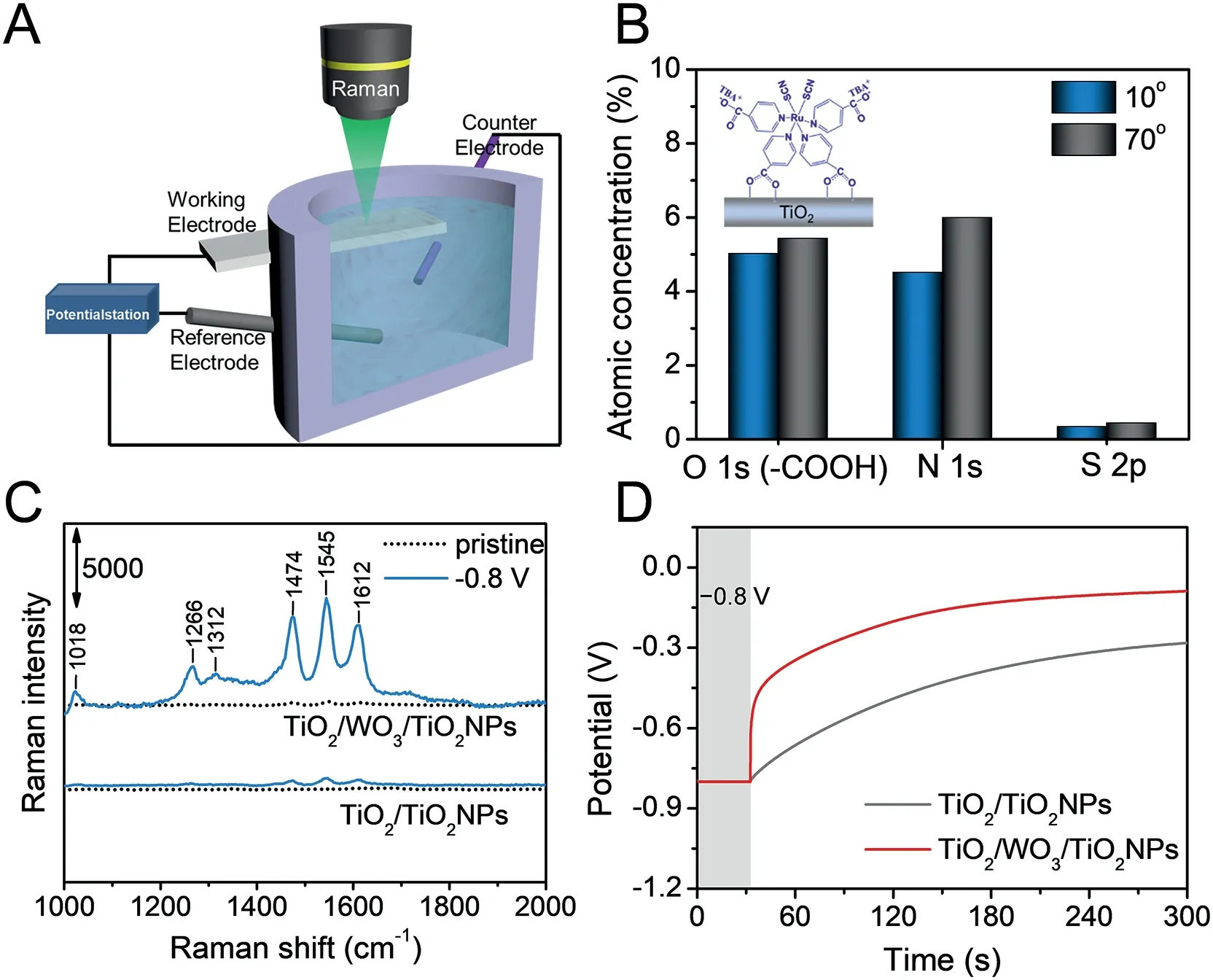
Fig.2.(A)Schematic of the electrochemical-SERS setup used in this study.(B)Atomic concentrations of N719 modified TiO2/WO3/TiO2NPs at take-off angles of 10°and 70°(inset:orientation of N719 on the sample).(C)SERS spectra of N719(3×10⁻³ mol/L)on pristine and VO-contained TiO2/WO3/TiO2NPs and TiO2/TiO2NPs.(D)Potential recovery of TiO2/TiO2NPs and TiO2/WO3/TiO2NPs after applying the negative bias voltage of−0.8 V for 30 s.
As a proof-of-concept,the Raman spectra of N719 onto TiO2/WO3/TiO2NPs werein-situcollected in HCl electrolyte by using a custom-built electrochemical cell(Fig.2A).In this study,the NPs samples were exposed to a negative potential for 30 s to introduce VOin the substrate,and the Raman signals were then acquired at the open circuit potential.Considering the energy match between the incident photons and the absorption spectra of N719(Fig.S11 in Supporting information),a 532 nm laser was chosen as the excitation light source for the Raman measurements.The orientation of N719 on the TiO2surface was investigated using an angle X-ray photoelectron spectroscopy(XPS)at the take off anglesθof 10°and 70°(Fig.S12 in Supporting information).As shown in Fig.2B and Table S2(Supporting information),the O 1s(−COOH),N 1s,and S 2p signals exhibit the higher atomic concentrations at 70°(bulk models)than those at 10°.Meanwhile,the atomic population on the N 1s signals at 70°is obviously higher than those on the O 1s(−COOH)and S 2p signals.These results suggest that the−SCN groups are oriented far away from the Raman substrates,and N719 molecules have been anchored onto the TiO2surface in the form of a bridged configurationviathe two carboxyl groups.Such bidentate coordination was considered to provide a favorable way for the CT between the substrate and adsorbed molecules[28].Compared to the faint signals collected on the pristine samples(see the dot lines in Fig.2C),the prominent signals of N719 molecules at 1474,1545,and 1612 cm−1,corresponding to a typical 2,2′-bipyridyl(bpy)ring stretching mode[29],were acquired on the VO-containing samples(the solid lines in Fig.2C).In Fig.2C,VO-TiO2/WO3/TiO2NT exhibits a higher SERS activity than VO-TiO2/TiO2NPs.This phenomenon can be ascribed to the WO3thin layer.Owing to the large optical modulation capacity,long-term durability,and memory effect of WO3,the coating of WO3onto TiO2can efficiently improve the electrochromic efficiency(Fig.2D and Fig.S13 in Supporting information).Furthermore,an excessively thick WO3film could result in a rough surface and the higher charge-transfer resistance(Figs.S14 and S15 in Supporting information)[30].Therefore the W-sputtering thickness in this study was optimized at 5 nm(Figs.S16 and S17 in Supporting information).
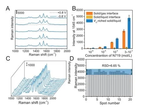
Fig.3.(A)SERS spectra of N719 adsorbed on TiO2/WO3/TiO2 NPs after exposed to the bias voltages of−0.8 V and+0.8 V alternately.(B)Raman intensity(at 1545 cm−1)of N719 on TiO2/WO3/TiO2NPs measured in air and in liquid.(C)SERS spectra of N719 collected from 20 randomly selected positions on VO-TiO2/WO3/TiO2NPs.(D)Intensity variation of the Raman peak at 1545 cm−1 in these 20 selected positions.
The role of VOon the SERS signal of the substrates was further investigated by repeatedly applying positive and negative voltages cycles.In Fig.3A,an enhanced N719 signal can be observed when applying the voltage of−0.8 V.In turn,switching the voltage to+0.8 V causes the weak Raman signals.The repeatable SERS activities were achieved by switching the voltages back to−0.8 V,verifying the VOcan be electrochemically tuned with satisfactory feasibility and reproducibility.Meanwhile,these results also allow one to conclude whether the weakened SERS activity is derived from the vanishing of VOrather than from the shedding or desorption of N719 molecules from the substrates.
To evaluate the application advantage of the proposed strategy in aqueous solutions,the Raman signals at 1545 cm−1(ν(C=C)(bpy),the stretching of the C=C bond in bpy)were collected at different N719 concentrations on TiO2/WO3/TiO2NPs in air and in aqueous solution(Fig.3B).Apparently,the Raman signals recorded in aqueous solution are much weaker than those acquired in air.Impressively,a 39-fold increase in the Raman signals was achieved from the SERS substrates with embedded VOunder a negative bias voltage.Notably,the Raman signals recorded on such a VOrich substrate in aqueous solution even exceeded those obtained in air.Moreover,the Raman signal was still conspicuous in the solution when the N719 concentration decreased to 10−6mol/L(Fig.S18 in Supporting information and Fig.3B),indicating high sensitivity of the VO-rich substrate.The enhancement factor(EF)of VO-TiO2/WO3/TiO2NPs was calculated to be 8.6×10⁴(Fig.S19 in Supporting information).Additionally,Fig.3C shows the Raman signals of N719 at twenty randomly selected regions on VOTiO2/WO3/TiO2NPs.The relative standard deviation(RSD)of the Raman peak at 1545 cm−1is determined to be 6.65%(Fig.3D),indicating excellent reproducibility of the VO-rich substrates.
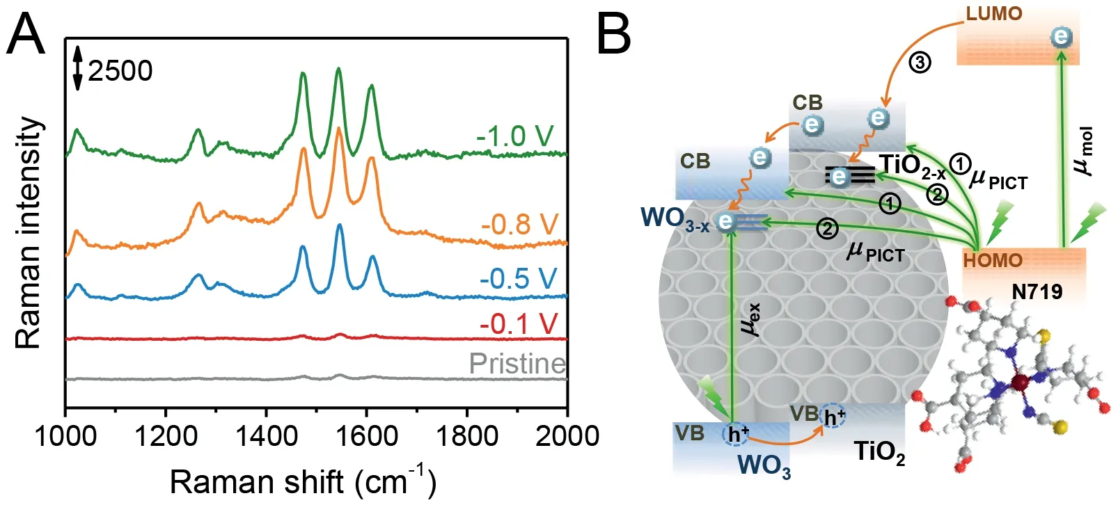
Fig.4.(A)SERS spectra of N719 on TiO2/WO3/TiO2NPs before and after exposure to different bias voltages.(B)Schematic energy level diagram and CT pathways in the N719-VO-TiO2/WO3/TiO2NPs system.
For a comprehensive understanding of the mechanism of VOinduced SERS activity,the Raman spectra of N719 were investigated under different voltages(Fig.4A).Owing to the increase in the VOcontent with increasing negative bias voltage,the Raman signal intensity from the substrates became substantially higher[26].The band structural analysis for VO-TiO2/WO3/TiO2NPs and N719 specimens was also carried out at different voltages(Figs.S20 and S21 and Table S3 in Supporting information).Compared to pristine samples,VO-TiO2/WO3/TiO2NPs exhibited the narrower bandgaps.The Mott-Schottky analysis also demonstrates that the charge-carrier density(Nd)calculated for VO-TiO2/WO3/TiO2NPs(3.45×1019cm−3)is larger than that of the pristine sample(1.84×1018cm−3),which is beneficial for the acceleration of PICT in VO-TiO2/WO3/TiO2NPs.Meanwhile,the contribution of CT in VOTiO2/WO3/TiO2NPs to the SERS signal of N719 was quantifiably determined based on the following equation[16]:
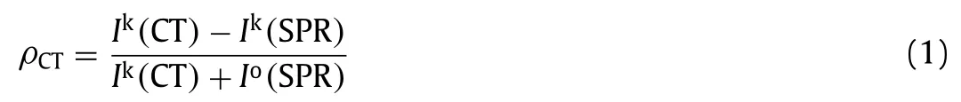
According to the SERS spectra in Fig.S22(Supporting information),the degree of CT(ρCT)of N719 was calculated as 0.41 and 0.69 for TiO2/WO3/TiO2NPs and VO-TiO2/WO3/TiO2NPs,respectively(details were provided in supporting Information).The key role of CT in our system was further demonstratedviaattaching other Raman probes onto TiO2/WO3/TiO2NPs by chemical bonding(4-MBA)or physical absorption(Ru(bpy)32+and 2,2′-Bipyridine)(Fig.S23 in Supporting information).Compared to 4-MBA,the SERS signals of Ru(bpy)32+and 2,2′-Bipyridine were poor and didnot exhibit obvious enhancement on VO-Ti O2/WO3/TiO2NPs.Moreover,the signal of N719 was remarkably dropped when a thin layer of SiO2film was covered onto TiO2/WO3/TiO2NPs before N719 modification to block CT between substrate and molecules(Figs.S24 and S25 in Supporting information).All these results indicate that CT plays an important role in the improved SERS signals after applying the negative bias.
Considering the location of the highest occupied molecular orbital(HOMO,−5.34 eV)and the lowest unoccupied molecular orbital(LUMO,−3.01 eV)of N719 molecules[31],the PICT could take place in following pathways(Fig.4B):(1)PICT from the HOMO of N719 to the CB of TiO2and WO3.The electrons can be directly excited from the HOMO of N719 to CB of TiO2(−4.21 eV)and WO3(−5.24 eV)[32]by an incident light of 532 nm(2.33 eV).(2)PICT from the HOMO of N719 to the defect levels(TiO2-xand WO3-x).In general,the defect levels induced by VOare usually located at∼0.5−1.0 eV below the minimum value of CB[33].As a result,PICT from HOMO of N719 to defect levels(TiO2-xand WO3-x)can provide more available PICT pathways than the sample that only contains TiO2and WO3,which can further lead to a magnification of the Raman scattering cross section,thus greatly magnifying the polarization tensor of N719 molecules.(3)Electrons in the LUMO of N719 transfer from the photo-excited N719 molecules to CB of TiO2.In addition,because of the existence of the defect levels(WO3-x),the band gap of WO3can be narrowed as 1.7−2.2 eV[33].Therefore,electrons can be excited from VB to WO3-x(μex)by a 532-nm laser and the photogenerated holes in WO3-xsubsequently transfer to VB of TiO2.Meanwhile,excited electrons in CB of TiO2transfer to CB of WO3.Therefore,a built-in electric field at the interface of TiO2and WO3with the direction of the electric field pointing from WO3to TiO2is formed.Driven by the built-in electric field,photogenerated electron-hole pairs can be effectively separated,realizing spatial charge separation and prolongating the lifetime of charge carriers,and thus enhancing the SERS activity[17,34-37].
To summarize,the electrochromic properties of the semiconductors were utilized to successfully produce the highly active SERS substrates that could be applied in aqueous electrolytes.Experiment data and theoretical calculation revealed that the abundant VOinduced by the electrochromic process facilitates the CT between the substrate and adsorbed molecules,thus enhancing their SERS activity.Especially,the as-proposed substrates were largely scalable,and their Raman signals were reproduced by controlling the applied bias voltage,thus providing an easily assessable and low-cost platform forin-situmonitoring of the reactions at the solid/liquid interfaces.
Declaration of competing interest
The authors declare that they have no known competing financial interests or personal relationships that could have appeared to influence the work reported in this paper.
Acknowledgments
This work was supported by National Natural Science Foundation of China(Nos.21874013,22074013 and 22073030),the Fundamental Research Funds for the Central Universities(Nos.N2105018 and N2005027),and the China Postdoctoral Science Foundation(No.2019M661109).The CPU time was supported by the Supercomputer Centre of East China Normal University(ECNU Public Platform for Innovation No.001).Special thanks are due to the instrumental or data analysis from Analytical and Testing Center,Northeastern University.
Supplementary materials
Supplementary material associated with this article can be found,in the online version,at doi:10.1016/j.cclet.2022.03.011.
 Chinese Chemical Letters2022年12期
- Chinese Chemical Letters的其它文章
- Diverse strategic approaches en route to Taxol total synthesis
- Recent advances in gold-complex and chiral organocatalyst cooperative catalysis for asymmetric alkyne functionalization
- Unmodified methodologies in target discovery for small molecule drugs:A rising star
- Recent advances in single-crystalline two-dimensional polymers:Synthesis,characterization and challenges
- Environmental applications of graphene oxide composite membranes
- Recent advances in the application of metal organic frameworks using in advanced oxidation progresses for pollutants degradation