
Recent advances in single-crystalline two-dimensional polymers:Synthesis,characterization and challenges
2023-01-30 06:48HoyongYngToZhngQunjiXue
Chinese Chemical Letters 2022年12期
Hoyong Yng ,To Zhng ,Qunji Xue
a Key Laboratory of Marine Materials and Related Technologies,Zhejiang Key Laboratory of Marine Materials and Protective Technologies,Ningbo Institute of Materials Technology and Engineering,Chinese Academy of Sciences,Ningbo 315201,China
b School of Chemical Sciences,University of Chinese Academy of Sciences,Beijing 10 0049,China
Keywords:2D polymer Single crystal Organic thin film Interfacial synthesis Structural characterization
ABSTRACT Two-dimensional polymers(2DPs)are emerging crystalline 2D organic material comprising free-standing,single-atom/monomer-thick,planar,and covalent networks with long-ranging structural order.Benefiting from their intrinsic porosity,crystallinity,and electrical properties,2DPs have displayed great potential for separation,energy conversion and electronic fields.In this mini review,we aim to provide the recent progress in crystalline 2DPs films form synthesis strategies to characterization methods,as well as the future trends.We first present the synthesis strategy of single-crystalline 2DPs films including crystal engineering approaches and surface science.Also,we summarize the characterization methods of 2DPs films and highlight the advantages and limitations of different methods focusing on chemical bonding,morphology,and crystal structure.Finally,we will present the current challenges and trends regarding the future developments of crystallinity,monomer design,synthesis strategy and characterization.
1.Introduction
With the development of science and technology,polymers play an increasingly important role in modern life.In 1920,Staudinger confirmed the existence of macromolecules and named them polymers and afterwards,Geeet al.synthesized independent polymer flakes by using air/water interface in 1935[1,2],extending the polymers into two-dimensional field.Novoselov and co-workers extract graphene with mechanical exfoliation for the first time in 2004,which triggered a research hotspot on graphene[3].Since then,the two-dimensional polymers with similar structures of graphene have aroused widespread interest(Fig.1)[4].
Subsequently,Schlüteret al.proposed the definition of twodimensional polymers(2DPs)that a 2DP can be represented as one monomer unit thick,covalently bonded molecular sheet with a long-range ordered(periodic)internal structure and provided the approaches to 2DPs in 2009[5].Different from the early polymer sheets,the key point of 2DPs is the definite periodicity in internal structure.Subsequently,a great breakthrough was made in 2DPs synthesis in 2012,when Kisselet al.synthesized 2DPs by organic synthesis method for the first time[6].Fig.2 shows the typical methods developed for the preparation of 2DPs in the past decades[6–11].Under the definition of two-dimensional polymers,there had several material systems in two dimensional,such as covalent organic frameworks(COFs)[12],Metal organic frameworks(MOFs),came into this emerging fields,making 2DPs been widely used in separation[13,14],energy conversion[15]and electronic fields[16].
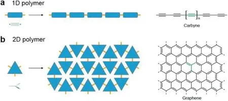
Fig.1.Different topologies of polymers.(a)A hypothetical linear monomer polymerizes into one dimensionally polymer.(b)A trigonal planar sp2-hybridized carbon atom polymerizes two dimensionally into graphene.Reproduced with permission[4].Copyright 2017,Annual Reviews.
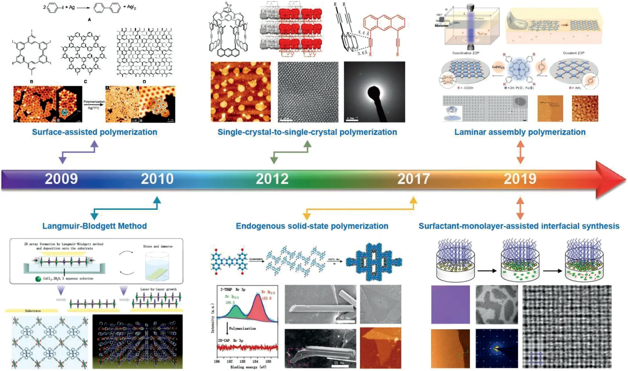
Fig.2.Timeline of important breakthroughs in the synthesis of 2DPs.Reproduced with permission[7].Copyright 2009,Royal Society of Chemistry.Reproduced with permission[8].Copyright 2010,Nature Publishing Group.Reproduced with permission[6].Copyright 2012,Nature Publishing Group.Reproduced with permission[9].Copyright 2017,Nature Publishing Group.Reproduced with permission[10].Copyright 2019,American Association for the Advancement of Science.Reproduced with permission[11].Copyright 2019,Nature Publishing Group.
The synthesis of 2DPs requires precise control of monomer arrangement before or during covalent bond formation to synthesis 2D supramolecular with periodic cross-linking network.Based on precise synthesis control and ingenious process design,several methods had been reported for synthesizing two dimensional crystalline polymers.To date,the reviews about the concepts[17]and structure[18]of 2DPs and related approaches have been reported[4],and this mini-review mainly focuses on the recent emerging strategies for the synthesis of single-crystalline 2DPs.Meanwhile,the characterization methods and challenges regarding single-crystalline 2DPs are also discussed.
2.Synthesis of single-crystalline 2DPs films
2.1.Single crystal-single crystal transition
The single crystal-single crystal transition(SCSC)is a method for synthesizing polymers based on topological chemical reactions in layered crystals,in which the growth sites of adjacent monomers are close enough and topological chemical reactions occur to form a cross-linked network based on covalent bonds,followed by chemical or physical exfoliation.As shown in Fig.3a,this approach is mainly divided into three steps:(1)crystallization of monomers to form a layered single crystal structure;(2)topological chemical reaction of the crystals to form connecting bonds;and(3)exfoliation of layered polymer crystals to obtain a single layer or multiple layers of 2DPs[4].This method can separate the monomer assembly from the bond formation process,using irreversible chemical reactions to form a crystalline product,and provides the possibility for the preparation of diverse connecting bonds and non-equilibrium structures[19].
In 2012,Kisselet al.[6]made a breakthrough in synthesizing crystalline 2DPs by using light-induced[4+2]cycloaddition dimerization(Figs.3b-d).In the synthesis process,the authors crystalized the specific monomers with photo-reactivity and then obtained the polymers crystal by photopolymerization,and the laminar structure resulting from a swelling process.Due to the decrease of crystallinity caused by the transition of molecules in the crystal from the monomerpseudo-laminar structure to the polymer laminar structure,this process is called the crystal-crystal transition process.If the lattice parameter changes little,no crack is generated or the crystallinity is decreased during the crystal transition,the process is called single crystal-single crystal transition(SCSC),which is necessary to find suitable monomers undergoing the process of topological chemistry.
In 2013,Bholaet al.[20]synthesized a 2DPs with a pseudolayered structure through photoinduced [4+4]cycloaddition dimerization using anthracene monomer(antrip).In the next year,Kisselet al.[21]prepared 2DPs by single crystal to single crystal conversion with similar monomer(Figs.3e-g).The monomer(fantrip)is composed of three light reactive tetra-fluoranthene branches connected through a core.After two-step photopolymerization,the polymer with molecular thickness of∼1 nm and pore size of∼9˚A was synthesized.In the process of monomer conversion into a binary polymer crystal,the lattice constant of the crystal,according to the topological reaction principle,changes little and does not lead to crack generation or crystallinity reduction,and the sheet of poly(fantrip)after exfoliation shows straight edges without obvious crack.
In the same year,Koryet al.[22]simplified the synthesis path on the basis of early research,and prepared centimeter-level 2DPs sheets(Fig.3j)by SCSC with designed monomer(Fig.3h),trying to overcome the limitations of accessibility,structural perfection and structural analysis.Since the polymerization process of the anthracene dimer in the polymer is reversible(Fig.3i),the species can be switched between two different states(monomer and sheet polymer)with little loss of crystallinity.Due to that the strong intermolecular interaction force in the crystal will lead to the diffi-culty of peeling,Langeet al.[23]provided a mild wet-exfoliated method to obtain single-layer or double-layer two-dimensional polymer films.As shown in Figs.3l and m,the 2DPs was synthesized by photochemical-induced[2+2]cycloaddition of designed monomer M1(Fig.3k),which also is the third case for SCSC.
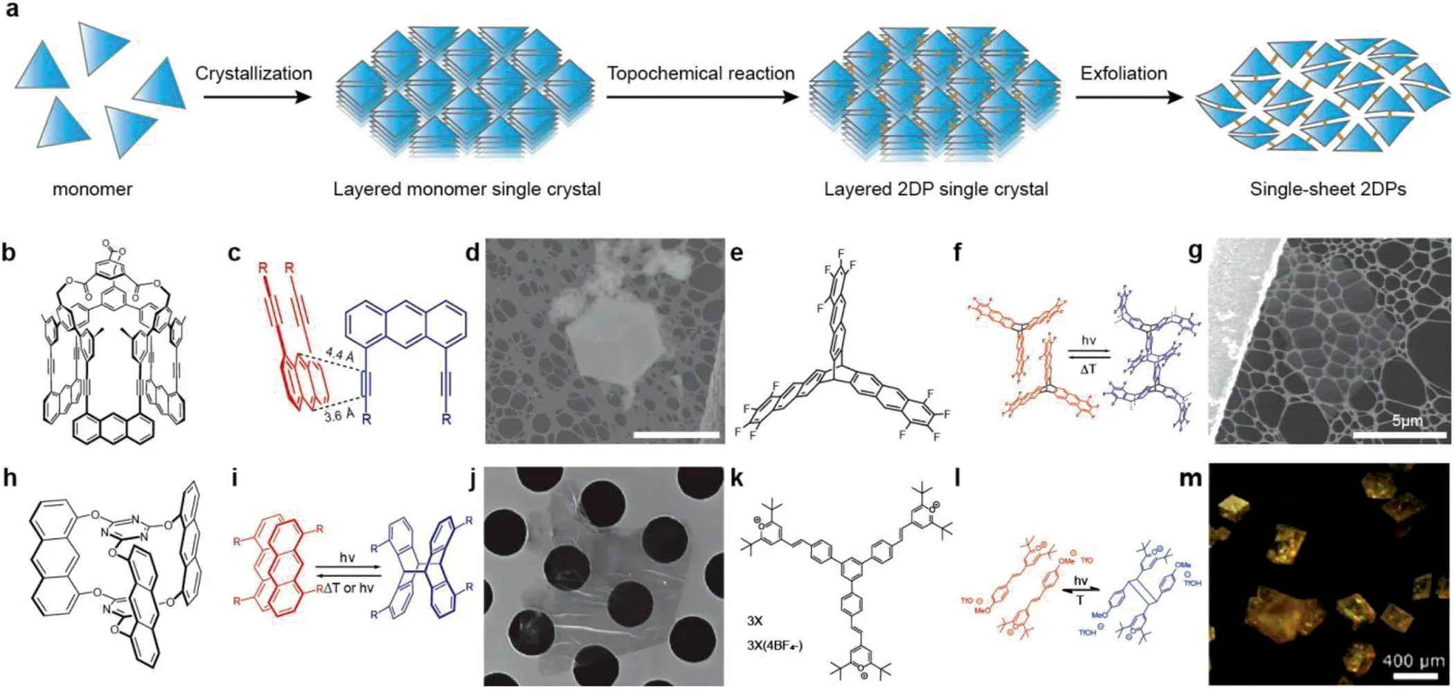
Fig.3.The single crystal-single crystal transition(SCSC).(a)Schematic illustration of the single-crystal approach for the synthesis of 2DPs with three steps.Reproduced with permission[4].Copyright 2017,Annual reviews.(b)A cup-shaped monomer structure.(c)The short distances between the alkynes and the cycloaddition positions of the adjacent monomers.(d)SEM micrographs of photo-irradiated monomer crystals.Reproduced with permission[6].Copyright 2012,Nature Publishing Group.(e)Chemical structure of the fantrip.(f)The photo-polymerization of the fantrip to the 2DPs.(g)SEM image of a sheet of poly(fantrip).Reproduced with permission[21].Copyright 2014,Nature Publishing Group.(h)Chemical structure of the anthracene-based monomer.(i)Topochemical photopolymerization of the monomer.(j)SEM image of a sheet composed of a few 2DPs.The hole size of the Quantifoil TEM grid is 2.5μm.Reproduced with permission[22].Copyright 2014,Nature Publishing Group.(k)Chemical structure of the monomer M1.(l)The model reaction of the designed monomer.(m)Optical microscopy images of small crystals of polymer after the topochemical reaction.Reproduced with permission[23].Copyright 2017,American Chemical Society.
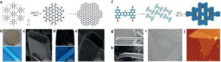
Fig.4.Synthesis and characterization of 2D PANI and 2D-CAP.(a)Schematic representation of 2D PANI formation.(b)Digital photograph of HAB crystals and optical microscopy image of a needle-like HAB crystal before annealing.(c)SEM image of an HAB single crystal before annealing.(d)Digital image of HAB and optical microscopy image of 2D PANI crystal after annealing at 500°C.(e)SEM image of a 2D PANI single crystal after annealing.Reproduced with permission[24].Copyright 2016,National Academy of Sciences.(f)Synthesis and characterization of 2D-CAP via endogenous solid-state polymerization.(g)SEM image of 2-TBQP crystals.(h)SEM image of the asprepared 2D-CAP crystals.(i)TEM image of an exfoliated 2D-CAP sheet.(j)Atomic force microscopy(AFM)topography of the triangular sheet.Reproduced with permission[9].Copyright 2017,Nature Publishing Group.
Apart from the light-induced polymerization of monomer in crystal,heat-induced reaction is also applied to transfer the monomers crystal into polymer crystal.Mahmoodet al.[24]synthesized atomically well-defined 2D polyaniline(2D PANI)via the direct pyrolysis of hexaaminobenzene trihydrochloride(HAB)single crystals in solid state(Fig.4a).After annealing at 500°C,the well-defined hexagonal HAB crystal(Figs.4b and c)directly pyrolyzed into highly stable,rigid hexagonal rods(Figs.4d and e),which was a layered graphitic structure and a winkled morphology revealed by high resolution scanning electron microscopy(HRSEM).By combing scanning tunneling microscopy(STM)and scanning tunneling spectroscopy(STS),the topological and electronic structures of the 2D PANI were revealed,which has highest conductivity of 1.41×10³S/cm after doped by hydrochloric acid(HCl).
Liuet al.[9]reported the preparation of a 2D-conjugated aromatic polymer(2D-CAP)by converting the pre-arranged monomers bulk crystal to polymers crystal undergoing C-C coupling reaction,which was named solid-state topochemical polymerizations (Fig. 4f). After holding the 2,7,13,18-tetrabromodibenzo[a,c]dibenzo[5,6:7,8]quinoxalino-[2,3-i]phenazine(2-TBQP)monomers crystal at 520°C for six hours,it turned into a shiny gray needle-shaped polymer driven by endogenous solid-state polymerization(Figs.4g and h).Then,the crystalline polymers were mechanically exfoliated into micrometersized sheets with a thickness of 1 nm and a highly uniform pore size of∼0.6 nm(Figs.4i and j).By designing the structure of monomers with different positions of bromine substituents on a phenazine-derived scaffold,the same author synthesis another conjugated polymers following thermal debromination to induce C-C coupling reaction[25].Usually,it is difficult to synthesis 2D conjugated polymers based on C-C coupling reaction without the help of template.When the spatial positioning of radial sites designed by topological method,the cross-coupling are easy to happen with minimize rotations after debromination.In the process of crystal conversion,since thermal excitation or photo-induced reactions do not require the transport of substances,the crystal stacking is disturbed to a minimum so that a high-quality crystalline product can be obtained,in which the layered crystal polymer sheet connected by a weak interaction and no chemical crosslinking.Therefore,the crystal can be stripped into crystalline 2DPs sheets with physical or chemical stripping method,such as ultrasonic,shear stress,ion intercalation,exchange,electrochemical.
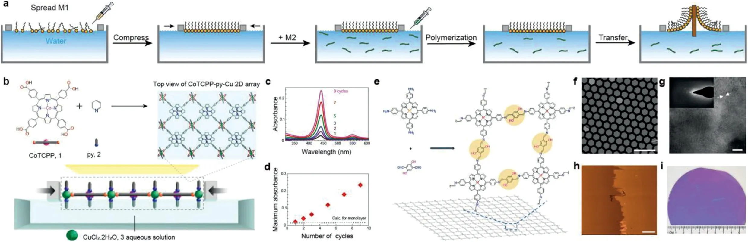
Fig.5.(a)Schematic illustration of chemical synthesis at air-water interface by Langmuir-Blodgett(LB)method.(b)Schematic illustration of the copper-mediated 5,10,15,20-tetrakis(4-carboxyphenyl)porphyrinato-cobalt(CoTCPP)2D array(CoTCPP-py-Cu).(c)Ultraviolet-visible absorption spectra of NAFS-1 films.(d)Plot of maximum absorbance of the CoTCPP Soret band versus the number of film growth cycles.Reproduced with permission[8].Copyright 2010,Nature Publishing Group.(e)Chemical structures of the monomers and 2DPs.(f)Scanning electron microscopy images of monolayer 2DPs suspended over a copper grid.(g)TEM,and(h)AFM images of a multilayer 2DPs.(i)Photographic image of monolayer 2DPs.Reproduced with permission[16].Copyright 2016,Nature Publishing Group.
2.2.Langmuir–Blodgett(LB)method
Langmuir-Blodgett method(LB method),as the most common method for air/water interface synthesis of 2DPs,can be dated back to experiments of Irving Langmuir and his student Katherine Blodgett in the 1920′s.As the synthesis process in Fig.5a shows,the monomers used in LB method are mostly amphiphilic molecules with polar head groups and nonpolar tail groups,so that the air/water interface can ensure the orientation of the amphiphilic molecules to form a directional arrangement.When the surfactant was introduced into reaction systems,a wider range of 2DPs can be synthesized with the guide of surfactant.Moreover,this strategy does not need physical/chemical exfoliation to obtain a layered polymer,which can synthesize film with the size equivalent to the water interface theoretically.
In 2010,Makiuraet al.[26]presented a solution-based growth strategy to fabricating perfectly crystalline MOF thin film with LBmethods,comprising metalloporphyrin building units and metal ion joints,as schematically shown in Fig.5b.After transferred onto the solid surface under mild conditions,the layer-by-layer films can characterize by ultraviolet–visible absorption spectroscopy(Figs.5c and d).By facile bottom-up fabricating the highly oriented MOF nanofilm,the author opened the way for the film in a range of important application,such as gas sensing,separation and low-pressure gas storage.Subsequently,Donget al.[27]have synthesized a 2D supramolecular polymer sheet containing bis-(nickel dithiolate)nickel complex at the air/water interface by LB method in 2015,whose size is in the order of square millimeter and the thickness of the single layer is 0.7–0.9 nm.The polymer formed by the coordination of Ni ion and thiol group ofπ-conjugated triphenylene hexanethiol monomer has excellent electrochemical performance,and the advantages of large area and single layer thickness make it suitable for high efficiency electro-catalytic hydrogen production.
With the development of the synthesis methods of 2DPs films,the size of the films prepared by LB method is also increasing.At present,researchers have synthesized wafer size thin films in the air/water interface,which has great application potential in the electronic field.Sahabudeenet al.[16]synthesized a crystalline polyimide film with a lateral size of 4 inches and a thickness of 0.7 nm at the air/water interface by Schiff-base polycondensation,and the Young’s modulus of the film reaches 267±30 GPa,which can be used as a thin film transistor in the field of microelectronics(Figs.5f-i).The monomer and polymer structures of the film are shown in Fig.5e.Firstly,tetra-(4-aminophenyl)porphyrin monomer was added to the sub-planar phase,and the surface pressure was adjusted to make it pre-arranged at the interface,then dihydroxyterephthalaldehyde monomer was added to the sub-planar phase so that it diffused to the interface and reacted with the prearranged tetra-(4-aminophenyl)porphyrin monomer to form imine bond,and finally the crystalline film was formed by polymerization.Schiff base polycondensation was first applied to the study of conjugated imine bonds formed by amine and aldehyde groups in covalent organic framework.Since the intermolecular hydrogen bonds formed in the imine center can enhance the structural stability,crystallinity and chemical sensitivity,it has been applied to the interfacial synthesis of two-dimensional crystalline polymer films.
2.3.Surfactant monolayer assisted interfacial synthesis
In addition to using surface pressure to adjust monomer alignment,surfactants also play an important role in the air/water interface-assisted synthesis process.Surfactant monolayer-assisted interfacial synthesis(SMAIS),which can provide a limited space for the growth of two-dimensional materials,plays a specific role in the nucleation and growth of materials,where surfactant is used as a template for the synthesis of 2DPs at specific interfaces.
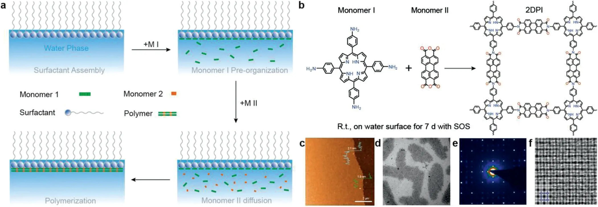
Fig.6.(a)Schematic illustration of chemical synthesis at air-water interface assisted by Surfactant monolayer.(b)A reaction scheme illustrating the synthesis of 2D polyimide(2DPI).(c)An AFM image of the 2DPI film.The traces in green and cyan are AFM height profiles at two selected positions,showing a thickness of∼2.0 nm,room temperature.(d)An overview of the 2DPI film obtained by bright-field TEM.Dark regions are crystalline.(e)A SAED pattern from the crystalline domain in(d).(f)An AC-HRTEM image of 2DPI.Inset:a simulated image of 2DPI along the[001]projection with the structure model overlaid.Reproduced with permission[11].Copyright 2019,Nature Publishing Group.
As shown in Fig.6a,the surfactant can spontaneously assemble at the interface to form a stable structure,then the orderly and close-packed structure control the anisotropic growth of twodimensional materials after injecting the monomers sequentially.In addition to increasing the lateral size of the product,surfactants can also assist in the synthesis of high crystallinity films with large domain sizes.In 2019,high crystallinity two-dimensional polyimide film was obtained with a thickness of∼2 nm(five layers)and an average domain size of∼3.5μm2by SMAIS(Figs.6b-d)[11].The function of the surfactant is to promote the horizontal or vertical alignment of the monomers with respect to the water surface,which in turn promotes their polymerization.The morphology,crystal structure,defects and order of the films were studied by optical microscopy,transmission electron microscopy,selectedarea electron diffraction(SAED)and other methods.Based on the above techniques,the accuracy of the results was verified and the aberration corrected high-resolution electron microscopy(ACHRTEM)images of the polymer materials were obtained(Figs.6e and f).The crystal structure and grain boundaries of the materials were analyzed at the molecular level of resolution.
With the development of synthesis strategy,Parket al.[28]synthesized 2D boronate ester covalent organic frameworks(2D BECOF)at the water/air interface with porphyrin monomer assisted by surfactant(SOS),whose single crystal domain size is about 60μm2(Figs.7a and b).Through the efficient synthesis method,a highly crystalline 2DPs film(Figs.7c and d)with excellent electrical properties can be integrated into an organic thin film/silicon nanowire-based field-effect transistor(FET)for the first time to simulate neuronal synapses.This opens up a new field for the development of emerging materials such as active ingredients in memory that can be used in future neuromorphological computing devices,which also offers possibilities for the future development of COF-based flexible wearable electronic devices.Besides,Sahabudeenet al.[29]have prepared a variety of crystalline 2DPs by SMAIS method(Figs.7e and f),which provided a controlled synthesis method of large-area crystalline 2DPs,and revealed the relationship between structure and properties,providing a basis for the further development of semiconductor 2DPs films.The intrinsic electronic properties of polyimine-based 2DP(PI-2DP)films with porphyrin structure were measured by ultraviolet photoelectron spectroscopy and terahertz spectroscopy,which display the band gap of PI-2DP films of 1.38 eV and the mobility of 0.01 cm−2V−1s−1.In addition,the average chip size of the PI-2DP film is up to 150 nm determined by transmission electron microscopy,and the crystal structure of the material is characterized by high-resolution electron microscopy(Figs.7g-i).As mentioned before,the SMAIS strategy can synthesis covalent–organic frameworks or crystalline polymers,which can be used in variety fields with excellent performance.Recently,micrometer-sized single-crystal COFs ribbons was also been synthesized by SMAIS,showing the applicability of this method[30].
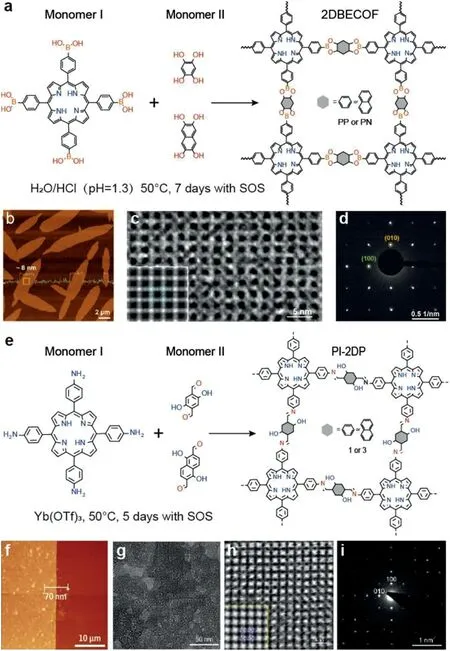
Fig.7.(a)A reaction scheme illustrating the synthesis of 2D BECOFs.(b)Enlarged AFM image of crystalline domains on film.(c)Enlarged HR-TEM image.Insets are lattice-averaged image calculated from the DFT and experimental electrondiffraction patterns,respectively.(d)Experimental electron-diffraction patterns.Reproduced with permission[28].Copyright 2020,John Wiley and Sons.(e)A reaction scheme illustrating the synthesis of PI-2DP.(f)AFM image of PI-2DP.(g)TEM image showing the increased average domain size up to∼150 nm.(h)HRTEM image showing the square lattice with significantly reduced distortion(Inset:simulated HRTEM image with the atomic model overlaid).(i)SAED pattern of a single-crystalline domain along the[001]direction of PI-2DP.Reproduced with permission[29].Copyright 2020,John Wiley and Sons.
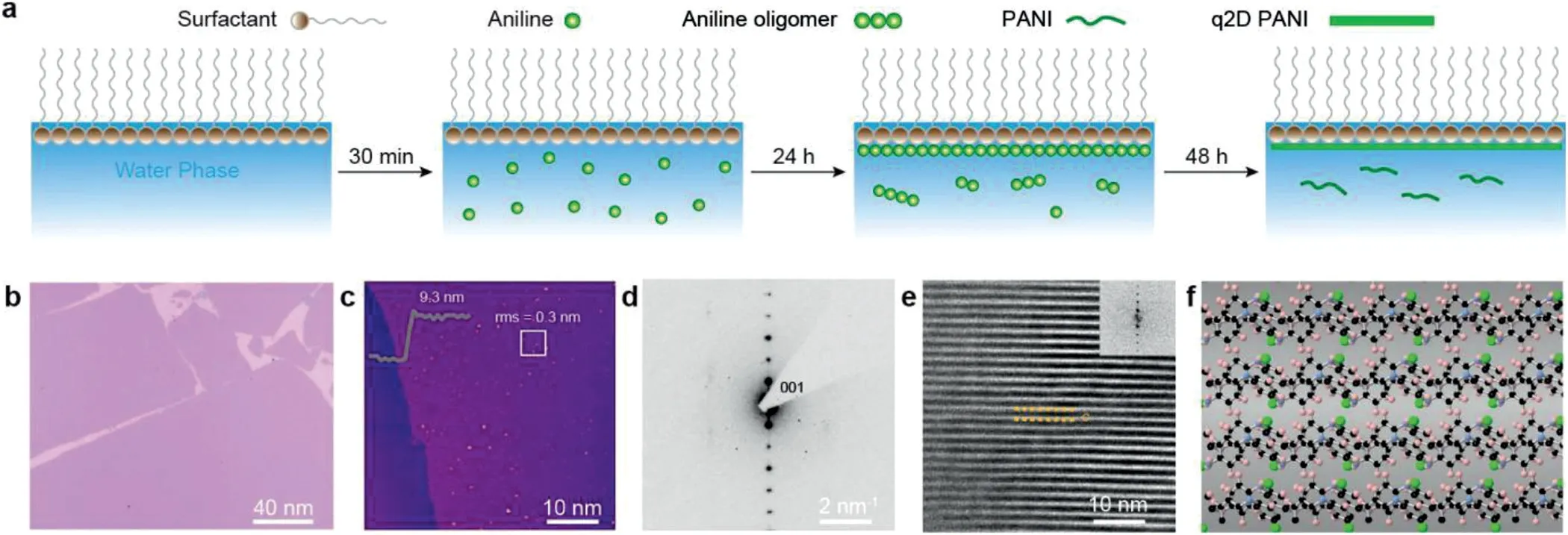
Fig.8.Synthesis of q2D PANI.(a)Schematic illustration of the synthetic procedure of q2D PANI:preparation of surfactant monolayer on the water surface;addition of aniline into water subphase and standing for 24 h for the diffusion of monomers to the water subphase and interface;introduction of HCl and ammonium persulfate(APS)to the water subphase;oxidative polymerization for 48 h.(b)Optical microscopy image of q2D PANI.(c)AFM image and height profile of q2D PANI.(d)SAED and(e)AC-HRTEM image of q2D PANI perpendicular to[001]axis.The two yellow lines mark out the interlayer distance c=13.41˚A.Inset of(d)corresponding fast Fourier transform(FFT).(f)Simulated atomic structure of the q2D PANI.Reproduced with permission[31].Copyright 2019,Nature Publishing Group.
Except for the 2DPs film synthesized from small molecular,surfactant assisted synthesis strategy also can guide the chain polymers into films.Polyaniline has excellent electrical conductivity and various chemical properties,while the synthesis of large-area and crystallization polyaniline films with thickness control have some challenges due to the complex molecular interactions between aniline oligomers.In 2019,Zhanget al.[31]synthesized polyaniline films with adjustable thickness(2.6–30 nm)and lateral size of∼50 cm2with the help of surfactants.The authors used a surfactant to align polymer chains at the air/water interface to form a uniform quasi-two-dimensional crystalline polyaniline(q2D PANI)film with average thickness of∼9.3 nm after 48 h polymerization(Figs.8a-c).Moreover,the PANI chains in the film exhibit excellent long-range order,in agreement with the simulated atomic structure(Figs.8d-f).When it came into application,the film showed good anisotropic electron transport ability with conductivity up to∼160 S/cm by hydrogen chloride doping.Moreover,the film also could be applied in high-performance flexible on-chip micro-supercapacitors[32].
In addition to the synthesis of single-crystalline 2DPs by reversible reactions,the use of kinetically irreversible reactions for the synthesis 2DPs is both attractive and challenging.Recently,Fenget al.[33]synthesized few layers,large area,single-crystalline charged 2DPs by Katritzky reaction with the aid of monolayer surfactant on water surface.The film displays adjustable thickness of 2–30 nm and a lateral domain size up to 120μm2.So far,it has been demonstrated the SMAIS is a promising strategy for synthesizing single-crystalline 2DPs[10,28-31,33].However,there remain challenges in utilizing SMAIS:(1)The sodium oleyl sulfate(SOS)and its analogues have been found suitable for SMAIS to grow 2DPs single crystals,but further development of novel surfactant monolayer is needed;(2)Interestingly,the monomers for SMAIS are limited for the porphyrin-based monomers,which could be due to that these monomers have strong interactions with SOS at air-water interface[11,31].As such,both surfactant monolayer and monomers should be investigated simultaneously in the development of new SMAIS system;(3)In order to take the full advantage of this interfacial methodology,the mechanism of SMAIS needs to be further explored in the aid of state-of-the-art interfacial characterization techniques[34].
2.4.Interface assisted synthesis
The interface is a flat or curved space between two regions of space occupied by different substances or substances in different physical states,with the thickness of the order of microns typically.The unique physical or chemical properties of different interfaces can provide corresponding conditions for the synthesis of materials,such as:facilitating the lateral movement of monomers to guide the assembly of precursors,and limiting the direction of reaction to control the structure and morphology of final products.As for the interface-assisted synthesis of 2D materials,Donget al.[35]had summarized the progress on interfacial synthesis strategies and their advancements in the structural,morphological,and crystalline control at confined 2D space.Here,we mainly focus on the advanced large-scale interfacial synthesis strategy for singlecrystalline 2DPs film.
In traditional solvothermal approach,it is difficult to control the nucleation and aggregation of organic crystal,which are mostly polycrystalline powder-like materials.Although Evanset al.[36]have successfully synthesized single-crystal 2D borate covalent organic framework by separate nucleation and growth process,the materials obtained by this method are usually limited by the small domain size and the high defect density and difficult to overcome the defects of monomer migration limitation and product transfer.Be different form the singe solution environments,two immiscible fluids can form a sharp interface,providing confined space for the growth of 2DPs which can continuously grow to the centimeter level with sufficient space and be easily transferred to the substrate by slowly removing a liquid.In 2017,Matsumotoet al.explored the influence of trifluoromethanesulfonic acid metal catalyst on COF synthesis[37]at room temperature and then synthesized imine-linked COFs film,assisted with Lewis acid,at the oilwater interface[38].The addition of water plays an important role in the polymerization reaction occurring at the interface,which spatially segregates the catalyst as well as the monomer to cause site-selective polymerization.
By combining the liquid-liquid interface and LB method,Zhonget al.[10]synthesized monolayer wafer-scale 2DPs film at the pentane/water interface based laminar assembly polymerization(LAP).As shown in Figs.9a and b,the porphyrin monomers dissolved in carrier solvent were injected into the interface by micro-injection pump to form monolayers of metal organic frameworks with Cu2+linkers or covalent organic frameworks with terephthalaldehyde linkers(Figs.9c and d).This strategy can provide improved scalability and patterning capability over previous gas-liquid polymerization methods that formed wafer-sized covalent 2DPs[39]with good crystallinity(Figs.9e-h).By controlling the reaction rate at the liquid-liquid interface,Deyet al.[13]synthesized the crystalline COF polymer by Schiff base polycondensation at room temperature,which employed salt-mediated technique to slow the diffusion of the precursor to obtain a thermodynamically controlled crystallization reaction.In addition,metal organic framework(MOFs)materials generally require metal ions to bind to organic ligands,and thus can be synthesized in aqueous solutions and organic solution interfaces.Donget al.[40]reported a porous 2D MOFs film,synthesized in the interface of aqueous solution and trichloromethane solution,with direct infrared band gap of 0.25 eV and room temperature conductivity of 220 cm2V−1s−1.
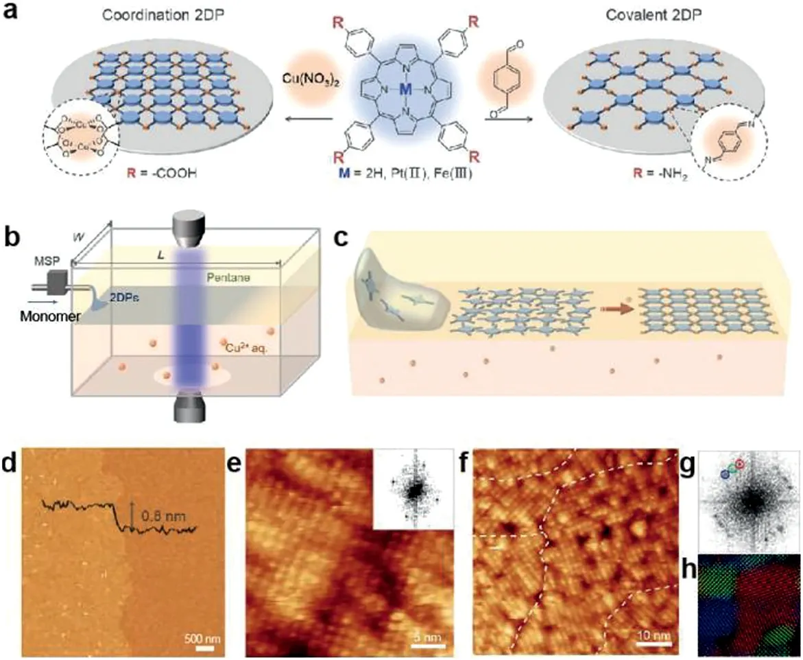
Fig.9.Laminar assembly polymerization.(a)Schematic of monolayer 2DPs and corresponding chemical structures of the molecular precursors.(b)Schematic of a LAP reactor and in situ optical characterization apparatus.(c)Schematic of the LAP synthesis that involves three phases.(d)AFM height image of monolayer 2DP.(e)Constant-current STM topography image of a single crystalline domain of monolayer 2DP on a thin film of Au(111)on mica.Inset:2D FFT of the image.(f)Constantcurrent STM topography image of multiple crystalline domains of monolayer 2DP II.(g)2D FFT of STM topography image showing square lattices of three major orientations.(h)Color-coded inverse 2D FFT image generated using the three sets of square lattice spots in(g).Reproduced with permission[10].Copyright 2019,the American Association for the Advancement of Science.
Moreover,few 2DPs based on carbon-bond had been synthesized in ambient condition.In 2016,Matsuokaet al.[41]reported a bottom-up synthesis of all-carbon,π-conjugated multilayer graphdiyne in liquid-liquid interface through a alkynealkyne homocoupling reaction.More successfully,the singlecrystalline graphdiyne nanosheets can be obtained in gas/liquid interface at room temperature.By sprinkling a very small amount of hexaethynylbenzene in a mixture of dichloromethane and toluene onto the surface of the aqueous phase,single-crystalline graphdiyne nanosheets were generated,which feature regular hexagonal domains,a lower degree of oxygenation,and uniform thickness(3.0 nm)and lateral size(1.5μm)(Figs.10a-e).
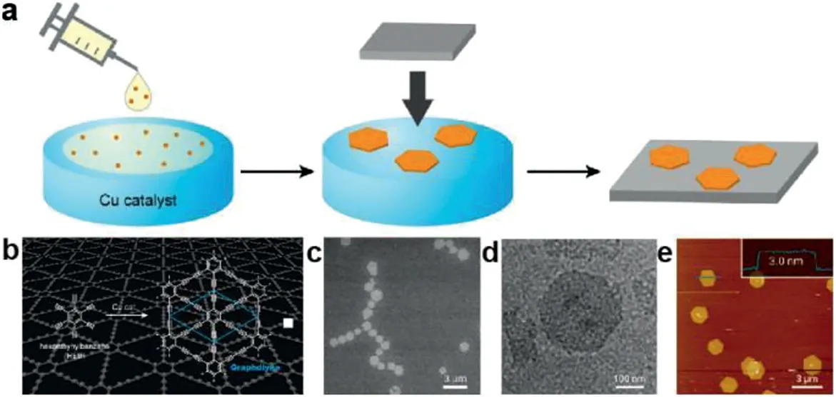
Fig.10.(a)Gas/liquid interfacial synthesis and microscopic observations of few-layer graphdiyne.(b)Chemical structure of hexaethynylbenzene(HEB)and graphdiyne.(c)SEM micrograph on silicon (100)modified with 1,1,1,3,3,3-hexamethyldisilazane[HMDS/Si(100)].(d)TEM micrograph on an elastic carbon grid.(e)AFM topographic image on HMDS/Si(100)and its cross-sectional analysis along the blue line.Reproduced with permission[41].Copyright 2017,American Chemical Society.
In liquid-solid interface synthesis,the 2DPs are usually guided by the specific material surface in reaction solution or the reaction solution is drop cast to the surface.When the solid interface is introduced into solution,the precursor in the liquid phase is physically or chemically adsorbed on the substrate surface and can be pre-organized along the substrate direction to provide a suitable orientation for growing.Dichtelet al.[42]reported the synthesis of 2D COF layered films on single-layer graphene(SLG)in solvothermal condition,which can grow in specific substrate for further analysis.Compared with grazing incidence X-ray diffraction(GIXRD)data of COF powders,the COF thin films showed improved crystallinity.The vertical alignment and long-range order of thin film growth on SLG make it more potential in organic electronic devices.Moreover,by adjust the properties of substrate,Songet al.[43]synthesized highly crystalline and oriented thin 2D conductive metal–organic frameworks(2D c-MOF)thin film with adjustable thickness,which combined layer-by-layer assembly method and functional substrates.Byin situgrowing organic spacer on the La0.67Sr0.33MnO(LSMO)electrode,the author demonstrated 2D c-MOF-based organic spin valves(OSV)with a vertical device structure for the first time.Compared with air-liquid and liquid-liquid interfacial synthesis,the liquid-solid interfacial approach allows direct device fabrication and characterization in specific substrate without transferring.Moreover,by controlling the concentration of precursor in the drop-cast process,it is possible to synthesis covalent films with tunable thickness.In 2015,Medinaet al.[44]synthesized several 2D COF films with tunable thickness at room temperature.The precursors were dissolved in polar solution and then drop-cast on a clean glass substrate for further vapor-assisted conversion,which played an important role in the formation of periodic structure.
Under the guide of solid template,two-dimensional polymers can be synthesized in atomically flat metal surface in ultra-high vacuum(UHV),where the specific direction and surface propertied can confine the polymerizationsviakinetic control[45].Various low-index noble metal surface,such as Au(111),Cu(111),Ag(111),had been used in surface-mediated polymerization,which was regarded as an effective bottom-up method for synthesizing conjugated molecular.Combined with various technologies,especially scanning probe microscopy,the process of monomer activation is detected,and the formation ofπ-conjugated skeleton is judged according to the change of substance absorption peak after the polymerization reaction.Nowadays,several classical methods and new reactions have been used to prepare 2DPs.
Ulman reaction is a kind of copper-catalyst C-C dehalogenation reaction and now it has been used in UHV to synthesis 2DPs in various substrates,such as Au(111),Ag(111),Ag(110)at high temperature.In 2007,Grillet al.[46]reported the synthesis of 2D covalent polymeric nanostructures by thermal activation of porphyrin building blocks in Au(111)at high temperature.By controlling the chemical structure of the building blocks and reaction process,a versatile route for future bottom-up construction of 2D conjugated network was reported(Figs.11a-d).Few years later,the same author synthesized layered covalently linked 2DPs films on Au(111)surfaces by selective and sequential activation of active sites with substrate-oriented growth[47].By introducing a specific weak molecular bond(halogen-carbon bond)into the monomer and dissociating the halogen atom without breaking the molecular bond by heating during the synthesis process,a reactive active point is generated,and then the active unit diffuses on the surface and form a covalent bond at the position of the previous halogen atom to connect with other units,thereby synthesizing a covalently bonded polymer on the surface.
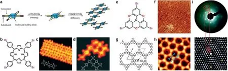
Fig.11.Surface-mediated polymerization.(a)Concept of the formation of covalently bound networks by connecting activated molecular building blocks.(b)Chemical structure of the tetra(4-bromophenyl)porphyrin(Br4TPP)molecule.(c)STM image(20×20 nm2)of a molecular island on Au(111)after deposition at low evaporator temperatures of 550 K prior to being activated.(d)STM image(8.5×8.5 nm2)of a network of eight molecular building blocks.Reproduced with permission[46].Copyright 2007,Nature Publishing Group.(e)Molecular structure of TBTANG.(f)STM images of P2 TANG on Au(111)kept at 210°C(90×90 nm2).(g)DFT-simulated P2TANG network.(h)STM images of P2TANG on Au(111)kept at 210°C(8×8 nm2).(i)Experimental and simulated low-energy electron diffraction(LEED)patterns of P2TANG/Au(111)at 210°C.Reproduced with permission[48].Copyright 2020,Nature Publishing Group.
As for the conjugated 2DPs,Bieriet al.[7]fabricated a covalently linked hydrocarbon superhoneycomb networks on Ag(111)surface.Under the surface-promoted coupling reaction,the hexaiodo-substituted macrocycle cyclohexa-m-phenylene(CHP)was fabricated and then the fully conjugated CHP network was obtained finally.with the discovery of conjugated 2DPs,it recently became possible to create virtually any lattice topology by stitching molecular building blocks of suitable symmetry together.Galeottiet al.[48]fabricated a mesoscale ordered two-dimensionalπconjugated polymers,whose electronic characterization reveals intriguing topological features.Most importantly,this 2DCPs is highly crystalline with domain dimensions greater than 100×100 nm2,which open opportunities for the synthesis of two-dimensionalπconjugated polymer Dirac cone materials(Fig.11f).By dosing the tribromotrioxaazatriangulene(TBTANG)(Fig.11e)onto an Au(111)surface,a highly ordered monolayer of 2DPs with large honeycomb was synthesized,in close agreement with the calculated dimensions of P2-trioxaazatriangulene(P2TANG)(Figs.11f-h).Be benefit from the sufficiently large domain size and low defect density of 2DPs,the authors prove the predicted electronic structure for these low-density 2DPs,and thus confirm that the lattice topology features the electronic band structure(Fig.11i).More information about surface-mediated polymerization is reviewed by Leonhard Grill[49].
3.Characterization of 2DPs films
Because of the complexity of the reaction and the particularity of the structure,the characterization of crystalline 2DPs has attracted much attention,including chemical bond formation,film morphology and internal structure.Each type of characterization methods presents its own pros and cons which are listed in Table 1 with the obtained information.
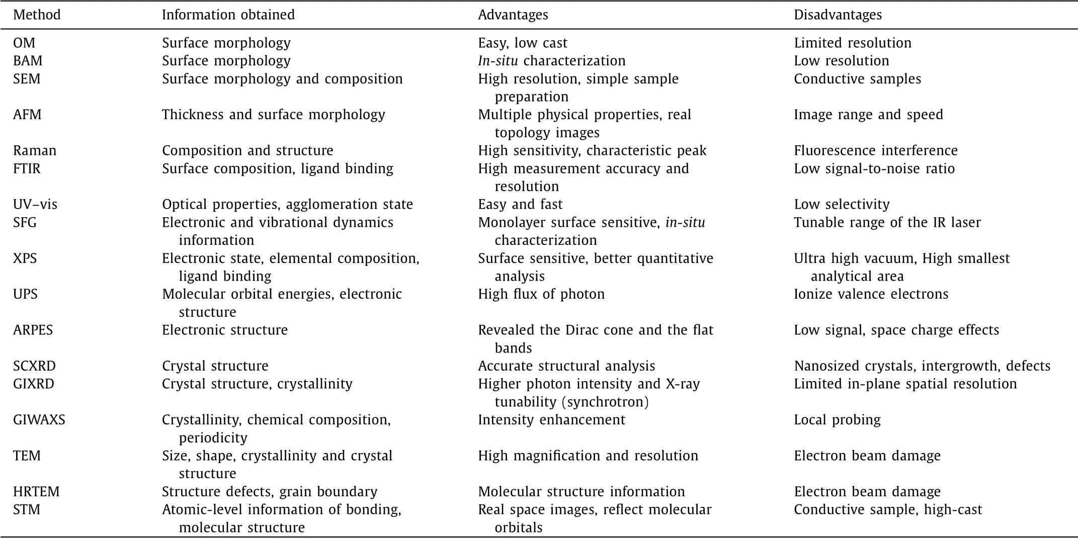
Table 1 The characterization of 2DP:Information,advantages and disadvantages.
3.1.Characterization of morphology
When the 2DPs film synthesized in the air-water interface,Brewster angle microscopy(BAM)canin-situcharacterize the response of film to surface pressure by monitoring the change of film morphology[50].However,the films synthesized at the interface need to be transferred to a specific substrate for further analysis,in which sufficient mechanical strength can make the polymers produce less structural changes and distribute continuously.The thin film is usually transferred onto a SiO2/Si substrate for optical microscopy analysis and atomic force microscopy(AFM)analysis to measure the size and thickness information of the thin film.When transferred onto solid substrate,the contrast between the substrate and the film can be used to distinguish the uncovered areas,to facilitate measurement of the film size[51]and reflect the uniformity of the film.
Unlike optical microscopes,which have limited resolution,scanning electron microscopes(SEM)can analyze the morphology of larger areas with higher resolution.When transferred to the copper mesh for SEM analysis,the thin film with less mechanical stability cannot fully cover the single mesh and the corresponding collapse occurs.For covalent polymers films,more than 65%of the molecules in the lattice region are connected with covalent bonds according to the percolation theory,so the film has sufficient mechanical stability.And the crack occur accidentally in copper mash can be a sign for identifying the film.The thickness and roughness of films are measured by AFM at atomic resolution and various surface properties can be measured by modifying the tip,such as adhesion,elasto-adhesive relationship and mechanical properties.In AFM images,the crack or edge location of the film is usually used to measure the thickness and roughness of specific areas.Similar to AFM,scanning tunneling microscopy(STM),as a probe-based analysis technique,can be used to characterize the surface of materials with local high resolution.Different from the contact analysis of traditional atomic force microscopy,STM can obtain the local electron density information and the surface morphology of covalent monolayer through the quantum tunneling effect between the probe and the sample surface[12].For polymer materials prepared on conductive surfaces,the structural information of the molecules can be directly obtained by STM to detect the reaction progress.
In addition,in-situcharacterization,as a time-dependent technique,can reflect the morphological changes of materials during polymerization.Zhonget al.[10]operated the optical system to characterize the reaction systemin situ,which showed the morphology of film in synthesis process of different stages:injection,self-assembly and polymerization.Through measuring the synthetic film area quantitatively,the author showed the relationship between the area and the amount of monomer solution,which is beneficial to control the synthesis process by adjusting the amountof monomer injection.For the longer time reaction,the material can be analyzed in different time periods.Kaushiket al.[13]characterized the morphology of the film in different time periods with electron microscope,which showed the process of fibrous to polymer thin layers through covalent bonds.
3.2.Characterization of chemical bonding
The characterization of the bond formation and the structure change in the reaction process is helpful to understand the polymerization mechanism and optimize the synthesis method.Infrared reflectance absorption spectroscopy(IRAS),Tip-enhanced Raman spectroscopy(TERS),ultraviolet-visible spectroscopy(UV–vis)and X-ray photoelectron spectroscopy(XPS)are commonly used to characterize the formation of bonds in polymers and calculate the conversion rate.Infrared spectroscopy and Raman spectroscopy,as non-contact characterization sensitive to bond formation,can characterize the formation of different bonds in the polymerization process.
By combined with scanning probe microscopy,TERS can analysis bulk materials and identify specific chemical components in nanometer scale.Mülleret al.[52]systematically studied the structure of 2DPs through[4+4]cycloaddition reaction of the monomer(Fig.12a)at air/water interface and characterized the information of polymer after transferred onto Au(111)substrate by TERS.According to the difference between the Raman spectra of the monomer and the thin film,the specific peak can be used as a marker of polymerization(Fig.12b),which can quantify the conversion rate of polymerization and provided directed spectroscopic evidence of crosslinks formed.In addition,based on the signal intensity ratio of the peaks in the Raman spectra of polymers,the Raman graphs were obtained to show the distribution of groups and defects,revealing the uniformity of polymer films(Fig.12c).Combing with various technologies,this study was able to systematically study how the reaction conditions affected the conversion and extended crystallinity during polymerization.
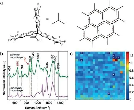
Fig.12.(a)Chemical structure of the monomer and the Packing model.(b)Normalized average TER spectra of monolayers of monomer and the polymer made from it deposited on Au(111).(c)Polymer TERS map measured over a 100×100 nm2 area with 5×5 nm2/pixel based on intensity ratio of the signals at 972 and 670 cm−1.Reproduced from with permission[52].Copyright 2017,John Wiley and Sons.
Similarly,UV–vis as well as fluorescence spectroscopy can be used as simple analytical method to detect the formation of polymer bonds.By measuring the electron transfer information in the monomer and polymer,the ultraviolet-visible spectrum can show the structural difference between the monomer and the polymer.While the fluorescence spectrum has high sensitivity and no damage to films,it can be used for detecting the formation of specific bonds.The formation of the conjugate network is indicated by the red shift of specific peaks in the UV–vis and fluorescence spectra.However,it is difficult to probe interfacial polymerization process using typical UV-visible and infrared(IR)spectroscopic techniques.Surface-specific vibrational sum-frequency generation(SFG)spectroscopy,as an interface-specific,molecular-level technique,could be used to understand the details of the on-water reaction mechanism.Sekiet al.[34]clarified how the polymerization reaction occurs at the water surfaces by tracking thequasi-2D polyaniline film generation process usingin situSFG(Fig.13a).By comparing the SOS-water and air-water interfaces,the authors revealed the charge of the surfactant monolayer on the water surface is key factor for generating highly conductive and crystalline PANI film(Fig.13b).
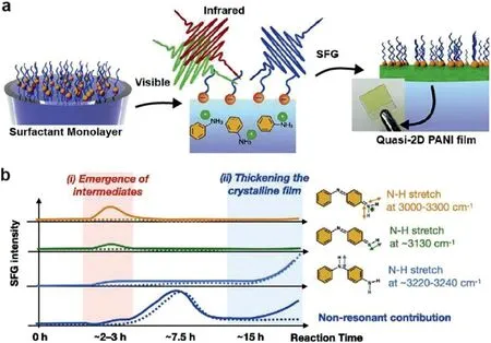
Fig.13.(a)Schematic illustration of the in-situ sum-frequency generation spectroscopy to follow on-water chemical reaction.(b)The corresponding time evolutions of the measured SFG signal.Solid and dotted lines represent the measured SFG signal evolution at the SOS-water and the air-water interfaces,respectively.Reproduced with permission[34].Copyright 2021,Elsevier Inc.
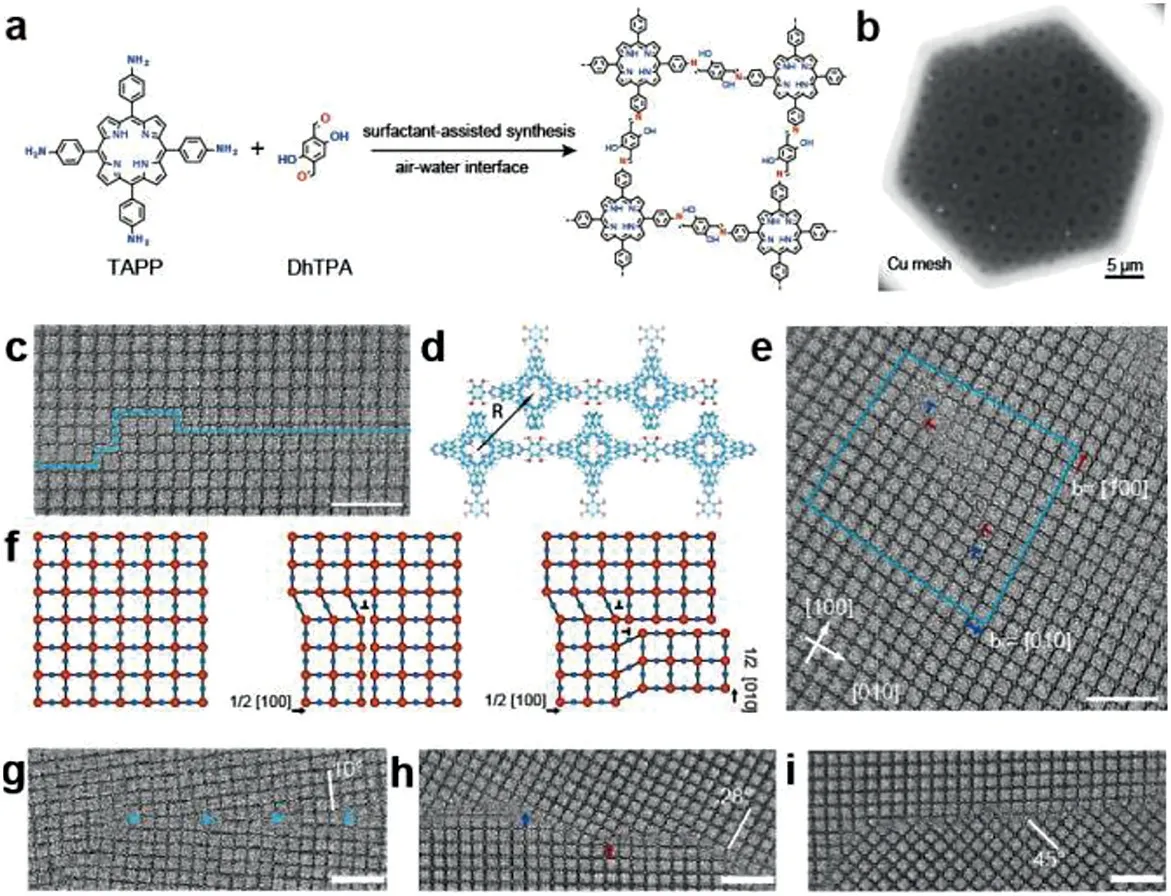
Fig. 14.(a) Reaction scheme of Schiff-base condensation between 5,10,15,20-tetrakis(4-aminophenyl)-21H,23H-porphyrin (TAPP) and 2,5-dihydroxyterephthalaldehyde(DhTPA).(b)Scanning electron microscopy(SEM)image of the freestanding L-2D-PI thin film.(c)Antiphase boundary(APB).(d)Schematic of the APB.(e)APB bounded with partial dislocations.(f)Schematic of APB formation via two nonlinear partial dislocations.The red and blue spheres represent TAPP and DhTPA units,respectively.(g)Low-angle grain boundaries(LAGB)with a misorientation of 10°.(h)High-angle grain boundaries(HAGB)with a misorientation of 28°.(i)HAGB with a misorientation of 45°.Scale bars:10 nm.Reproduced with permission[53].Copyright 2020,the American Association for the Advancement of Science.
In addition,X-ray photoelectron spectroscopy(XPS)and ultraviolet photoelectron spectroscopy(UPS)can also be used to characterize the polymerization process.XPS can obtain chemical information related to thin films,such as elemental composition,concentration and chemical information of surface and nearsurface atoms,while UPS can characterize critical formation with lower energy.XPS can be used to analyze the strength of different bonds when the spectra of monolayer and multilayer films are similar[16].Moreover,Angle-resolved photoelectron spectroscopy(ARPES),as a standard technique to probe the electronic structure,can revealed the Dirac cone and the flat bands of conjugated polymers[48],facilitating the characterization of the electronic band structure of fully conjugated polymers.
3.3.Characterization of crystal structure
Transmission electron microscopy(TEM)remains one of the primary methods for obtaining direct crystal structure and atomic scale information of 2DPs.Using TEM as a tool for crystal structure analysis,several types of information can be obtained,such as the image of molecular structure,the interplanar spacing of stacking layers,and the grain boundaries or size of the domain.By combining several characterization methods,such as GIXRD,the relationship between material structure and properties has been further understood.
Usually,because of the high sensitivity of polymer to electron beam,it is difficult to extract sufficiently information under the impact of electron beam,electrostatic charge and chemical etching.In order to reduce the influence of electron bean,Donget al.[27]performed SAED on the film at−175°C and adopted the corresponding synthetic powder sample to indirectly prove the internal structure of the film sample.On the other hand,graphene was used to encapsulate the film to form a sandwich structure in lowdose diffraction technology to protect the film from electron beam damage[16].Combined with density functional theory,the crystal structure of the material can be verified.
Moreover,the high-resolution transmission electron microscopy(HRTEM)has been widely applied to analyze the morphology,crystal phase,crystal domain,grain boundary and defects of films.By using AC-HRTEM,Liuet al.[11]obtained two-dimensional polyimide film molecular-level resolution lattice images with an average chip size of∼3.5μm2in 2019.Similarly,Sahabudeenet al.[29]obtained a lattice image with less distortion in HRTEM,which clearly shows the arrangement of porphyrin units,and the crystal domain size of the porphyrin units is∼150 nm measured by TEM images.Under high crystallinity of 2DPs films,an image of the polymer skeleton can be observed as the electron beam passes in a particular direction,and discrete bright diffraction spots can be observed in the SAED[12].When the resolution of TEM image reaches below 0.05 nm,it is necessary to introduce an aberration corrector to reduce the influence of defocusing and astigmatism in electron microscope.Be beneficial from the AC-HRTEM,Qiet al.[53]observed the grain boundaries in a layer-stacked 2D polyimine film(Figs.14a and b)near atomic scale,which revealed the formation mechanisms and potential influence to functions.Moreover,the AC-HRTEM image provided directly elucidation of grain boundaries(GB)structures and formation mechanisms in 2DPs(Figs.14ci),laying a solid foundation for characterizing organic 2D material.Usually,the parameters of TEM should set carefully because of the strong interaction of electron beam and hydrogen atoms in organic material.By determining the correlation of resolution and electron dose,the authors reveled the functions between diffraction spots intensity and electron dose.Under the condition of ensuring the resolution,reasonable parameter setting can keep the balance of electron dose and image contrast and proper operation can facilitate the high-resolution image of films,which is consistent with the simulated results.
Due to the weak interaction between the X-ray and the material,the diffraction signal of the film and the substrate is collected after penetrating the sample.The grazing incidence method is usually used to change the angle between the X-ray and samples to change the penetration depth of the X-ray beam,giving detailed information of the thickness and periodicity of the thin film.According to the interaction between X-ray and sample,it can be divided into GIXRD and grazing incidence wide-angle X-ray scattering(GIWAXS),and based on these two techniques,the structure information of samples with different scales can be analyzed.
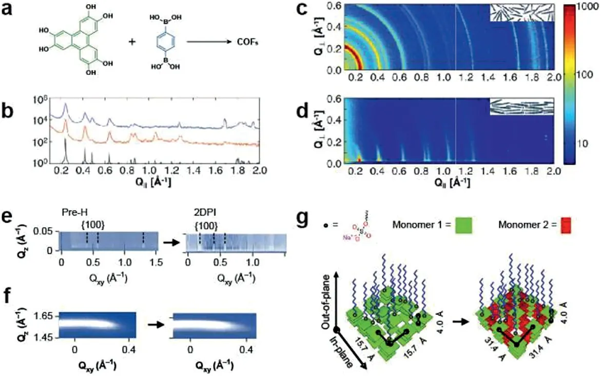
Fig.15.GIXRD and GIWAXS analysis of film.(a)Solvothermal condensation of 2,3,6,7,10,11-hexahydroxytriphenylene(HHTP)and 1,4-phenylenebis(boronic acid)(PBBA).(b)Projections of GIWAXS near Q┴=0 in(c,d),and the simulated powder diffraction spectrum(bottom/black).(c)X-ray scattering data obtained from COF powder;(inset)schematic of randomly oriented COF-5 grains in the powder.(d)GIXRD data from a COF film on(SLG/Cu);(inset)schematic of oriented COF grains in the film.Reproduced with permission[42].Copyright 2011,the American Association for the Advancement of Science.In-plane(near Qz=0)(e)and out-of-plane(near Qxy=0)(f)diffraction patterns,demonstrating the transition from pre-H to 2DPI.(g)A schematic of the pre-H to-2DPI transition.Reproduced with permission[11].Copyright 2019,Nature Publishing Group.
After synthesizing the oriented 2D layered COF films on SLG surfaces,Colsonet al.[42]employed the GIXRD to demonstrate the structure of films(Fig.15a),in which the substrate surface is nearly parallel to the incident beam.The synchrotron X-ray diffraction of the COF films and powders were shown in(Figs.15c and d),and the diffraction spectrum(Fig.15b)shows the improved crystallinity of film compared with COF powders.Similarly,GIWAXS,as an Xray diffraction method,is perfectly suited for the investigation of the material crystallinity of surfaces and thin films.As the previous literature reported,GIWAXS can be used to demonstrate that thin films are highly crystalline and non-oriented[38],to measure the thickness of superlattice repeat units[10],and to measure the lattice constant of crystalline thin film units[31].Compared with the SAED measurements and the DET simulation results,the polymer was measured by GIWAXS method to clarify the molecular stacking pattern of PI-2DP and verify the correctness of the results.Zhonget al.[10]used the GIWAXS technique to prove the polycrystalline structure of single-layer 2D porphyrin polymer,which also combined with the FFT image to analyze the crystal orientation and measured the crystal domain size and boundary.By collecting the information of the samples at different angles of incidence and rotation,GIWAXS can determine the orientation of the films and the direction of the internal cells according to the variation of the characteristic peaks and the signal intensity.Moreover,GIWAXS was used to gain insight polymerization mechanism before(Fig.15e)and after(Fig.15f)the addition of second monomer under SMAIS synthesis strategy(Fig.15g).
4.Application of 2DPs films
The multilayer film synthesized at the interface,even a single layer 2DPs,can be easily transferred to different substrate for further application.Due to the high crystallinity and unique physical chemistry property,the single-crystalline 2DPs film is becoming increasingly important for their promising applications in separation,energy conversion,and electronics.
Laiet al.[54]synthesized crystalline 2DPs film through the LB method,which can be transferred to anodic aluminum oxide(AAO)porous support layer by layer,showing excellent solvent permeability for both polar and nonpolar organic solvent.In comparison to the amorphous film prepared by the same LB process,the water permeance of crystalline film is approximately 100 times higher.As for the energy conversion,Fenget al.[33]synthesized singlecrystalline charged 2DP(C2DP)film by SMAIS on water surface,which displays high chemical stability and possess robust framework structure because of irreversible linkages.Be benefit to the high density of well-defined cationic sites(∼8.8×10⁷m−3)and a high density of pores(∼1.1×10¹⁷m−2)combined with highly orderedquasi-1D channels,the C2DP shows great potential in osmotic energy conversion.The output power density of film can reach as high as 4 W/m2,which outperforms 2D material such as graphene and boron nitride.
To expand the application of 2DPs film in electronic filed,Fenget al.[16]synthesized a crystalline monolayer film at the air/water interface with a thickness of 0.7 nm and an excellent Young’s modulus of 267±30 GPA,which can be used as a thin film transistor in the field of microelectronics.The carrier mobility of polyimine film can be increased to 1.6×10⁻⁴cm2V−1s−1when doping with I2,which shows potential to be used as semiconducting material for thin-film transistor(TFT)under ambient conditions.As for the chemical sensor,the q2D PANI is a promising electrode material owing to the ultra-thinness and wide range of tunability of electric conductivity[31].When doping by hydrogen chloride,the film showed good anisotropic electron transport ability with conductivity up to∼160 S/cm.Compared with porous conducting polymer,the q2D PANI film with ultra-thinness and long-range ordered chain structure provide sufficient exposure of activity cite and efficient pathways for the diffusion of NH3molecules[51,52].Moreover,the few layers single-crystalline 2D BECOF-PP film synthesized through SMAIS can also be integrated into an organic thin film/silicon nanowire(SiNW)-based FET to mimic neuronal synapses owing to the facile thin-film processability and high mechanical stability,which provides possibilities for the future development of COF-based flexible and wearable electronics[28].Further applications of crystalline 2DPs films can be found in other reviews[12,55,56].
5.Trends and challenges
Single crystal conversion and interface-assisted synthesis can separate the monomer pre-organization step from the monomer linking step,both of which have important application potential in the synthesis of crystalline polymers.At present,it is important to control the crystal phase,grain size,grain boundary and edge structure in the synthesis of crystalline 2DPs.In the aspect of crystal phase control,reducing the area of amorphous region and increasing the size of crystal domain are development direction of crystalline 2DPs.Improving the crystallinity and crystal quality is beneficial to the characterization of polymer,and can expand the application range of 2DPs.After understanding the mechanism and the optimal crystallization condition,the crystallization process of the material can be controlled by a thermodynamic or kinetic method,and ordered crystal structure and large crystal size are expected to be obtained.
For the monomer,topological chemistry can be used to guide the structural design and monomer selection,combined with density functional theory calculations to systematically adjusting the properties of materials[57].At present,the synthesis of 2DPs is mainly based on reversible covalent bonding reactions,but nonreversible reactions can produce 2DPs with higher conjugation degrees.How to prepare fully conjugated 2DPs by coupling reaction and enlarge the crystal domain size of the products is an important challenge in this field.Benefited from the surface-mediated polymerization,the fully conjugated 2DPs with electronic topological properties have been now confirmed experimentally[58].Moreover,the manifold of designed building blocks in organic chemistry offers a huge variety of skeleton for possible lattice topology[59]and specifical function[60],combining with multiple synthesis strategies.Even under very mild condition,the Suzuki reaction can be employed to synthesis C-C bonded 2D conjugated polymers on liquid/liquid interface,which opened a door for 2D conjugated polymers[61].
For the characterization of the 2DPs structure,the analysis difficulty lies in the sensitivity of the material to the electron beam and the difficulty in preparing the electron microscope sample[62].Various characterization techniques can only provide partial material structure information,and need to obtain a comprehensive and representative structure information map,even in molecular or atomic scale.No matter what strategy is used to synthesize 2DPs,it is necessary to develop appropriate characterization methods to analyze the structure,long-range ordering,purity,defects and so on[19].By combining with the characterization of property,the relationship between the geometric structure and properties can be given,which can guide the material structure design for specific properties.
With the further development of material systems and characterization methods,we can use modular design strategies,improved synthesis strategies and morphological control to achieve the synthesis and even commercial application of 2D polymer materials.
Declaration of competing interest
The authors declare that they have no known competing financial interests or personal relationships that could have appeared to influence the work reported in this paper.
Acknowledgment
This work was financially supported by the Zhejiang Provincial Natural Science Foundation of China(No.LR21E030001).
 Chinese Chemical Letters2022年12期
- Chinese Chemical Letters的其它文章
- Diverse strategic approaches en route to Taxol total synthesis
- Recent advances in gold-complex and chiral organocatalyst cooperative catalysis for asymmetric alkyne functionalization
- Unmodified methodologies in target discovery for small molecule drugs:A rising star
- Environmental applications of graphene oxide composite membranes
- Recent advances in the application of metal organic frameworks using in advanced oxidation progresses for pollutants degradation
- Recent progress on two-dimensional materials confining single atoms for CO2 photoreduction