Design and Energy Estimation of QCA Based Simple Data Path Selector Cum Router Unit for Nano Communication
Angshuman Khan,Rajeev Arya
1 Department of Electronics and Communication Engineering,National Institute of Technology Patna,Bihar 800005,India
2 Department of Electronics and Communication Engineering,University of Engineering and Management,Jaipur,Rajasthan 303807,India
Abstract: Quantum dot cellular automata (QCA)is promising nanotechnology due to the three main advantages: faster speed,nanoscale size,and ultrasmall power consumption.This paper proposed a simple data path selector cum router as the ‘multiplexerchannel-demultiplexer’ unit using QCA,an unavoidable building block of nano communication.A Simple 2×2 block and the extended 4×4 block of data path selectors have been proposed in this article.The layouts of the proposed designs have been verified in QCADesigner,and the energy dissipation has been evaluated using two tools,QCAPro and QCQDesigner-E(QDE).The suggested designs reached a significant improvement in cell complexity(cell count)and covered area over the existing designs.In precise,the proposed 2×2(4×4)block shows 86%(63%)lower cell complexity and 87% (37%) smaller area than the prior reported similar designs.In addition,the currently reported 2×2 (4×4) unit has 86% (60%) lower QDE based energy dissipation compared with prior reported designs.
Keywords: nanocommunication; quantum dot cellular automata;router;switch
I.INTRODUCTION
Quantum dot cellular automata(QCA)is an emerging technology to design the logical circuits at nanoscale using Coulomb’s interaction property of electrons[1].Nowadays,nano communication system design using QCA is a popular trend for modern communication systems design and network analysis.Router,switch,etc.,are essential and unavoidable building blocks of communication systems and networks.The basic unit of a data path selector cum router for a communication system is the ‘multiplexer-Channeldemultiplexer’ module.This article aims to propose a ‘MUX-Channel-DeMUX’ segment using QCA for nano communication applications.It is a simple data path selector of a nano-router.A data is selected from one of the many data lines using a multiplexer.It is transmitted through a channel,and the transmitted data is now routed to any one of the output data lines using a demultiplexer.
In current work,the simplest type of QCA-based data path selector cum router unit has been designed using a 2:1 multiplexer,a QCA wire,and a 1:2 demultiplexer.Then the work has been extended to develop the next higher block with four input lines and four output lines.
The basic unit of the QCA circuit is a square boxshaped ‘cell’ consisting of four quantum dots at the four corners of the box with two free electrons [2].When the tunneling barrier between dots remains low,the electrons can travel between dots based on quantum mechanical effects.The electrons always try to stay at corner positions due to the Coulomb’s repulsion.It produces two stable states relatively,and two polarization levels represent states; polarization P=‘+1’indicates logical‘1’and polarization P=‘-1’indicates logical ‘0’ as shown in Figure 1.These QCA cells are used to design the basic building blocks like wire,inverter,and majority gate [3,4].QCA wire is an array of cells used to propagate signals from input to output,keeping the same polarization as shown in Figure 2.To flip the electrons’ positions or change the polarization states,QCA inverters are there,which can be formed by placing cells diagonally,as shown in Figure 3.A logic gate whose output attains the polarization of the majority of the inputs is known as the majority gate or majority voter,as shown in Figure 4.It is a three-input gate and works with the function M(A,B,C)=AB+BC+CA[5].It can form AND gate if it follows the logical function M(A,B,0)=AB with C=0,and it can form OR gate if it follows the function M(A,B,1)=A+B with C=1.
The primary source of signal transmission in QCA circuits is a clock that can decide the direction of information delivery and provides the energy to propagate signal information.No external supply or clock is required for QCA circuit operations;only internally applied clocks provide enough energy for information transmission[6].There are four zones of a QCA clock-cycle:switch,hold,release,and relax,as shown in Figure 5.QCA layout is implemented using the four zones mentioned above and 90 degrees out of phase to each other [3].The current work is a data path selector that can work as a router to route information.It is a communication network at the nanoscale between nanodevices.The multiplexer-demultiplexerbased single-layer sole design is the novelty of this work,and ultra-small energy dissipation is one of the main advantages of the proposed work.
II.EXISTING WORKS AND GAPS
A crossbar network using QCA was implemented long ago by Graunkeet al.in 2005[7].The designed circuit was a QCA wire-crossing network and was made using parallel to serial converters,registers,and latching devices [7].Then there was a long gap; in 2012,Das and De designed a multilayer design(4×4 size)data path selector cum router using 1:4 multiplexer and 4:1 demultiplexer.It utilized 419 QCA cells with a total area of 0.54µm2,and it had 3 clock cycles delay[8].In the same year,Liu et al.inspected both the best and worst cases for the aggressors to determine if QCA circuits are safe to power analysis attack [9].In addition to that,they presented the Serpent cipher design using QCA.In 2013,Sardinhaet al.designed a new nano-router architecture using a crossbar network,parallel to serial converters and demultiplexers[10].It was a 4×4 network that utilized 4026 QCA cells and 13.81µm2area.It had a massive delay of 48 clock cycles,and it was a multilayer design.Silvaet al.described the parallel-to-serial converter,serial-toparallel converter,hamming code checker,and parity checker using QCA technology in 2015[11].In 2017,Das and De projected a 2×2 circuit-switched network using multiplexers and demultiplexers with cell count 382.It exploited 1.02µm2area,and the input to output delay was 7-clock cycles [12].It was a singlelayer design,and it dissipated 687.8meVenergy.In the same year,Daset al.designed a 4×4 router using QCA demultiplexer and serial to parallel converter[13].It used 3351 QCA cells with 9.86µm2area.It was a single-layer design,and the input to output delay was 15-clock cycles.Again Das and De proposed polar encoder architecture using QCA in 2018[14].Next year,Daset al.designed an even parity generator and an even parity checker using the QCA XOR gate with reduced latency and lower cell count[15].
The above-discussed literature of QCA was very focused on nanocommunication related works.However,there are seldom works dedicated to data-path selectors or nanorouter in the QCA literature of nanocommunication.These include the works done by Das and De [8],Sardinhaet al.[10],Das and De[12],and Daset al.[13].Nevertheless,all these prior reported works suffer from high complexity,lack of simplicity,and missing detailed energy dissipation calculation in most cases.
The current work proposed a simple 2×2(and extended 4×4)data path selector cum router using 1:2 multiplexers and 2:1 demultiplexers.The energy dissipation analysis using two different methods,the signal flow diagram and the rigorous comparison with existing designs,have been used to make the work more significant.
III.PROPOSED DESIGNS
In the communication system,a data-path selector cum router which can be simply considered‘multiplexer-channel-demultiplexer’,is an unavoidable part of efficient channel utilization.It is the connecting part of the communication network between nanodevices.When many signals come from different sources,then data is selected from any one of the sources,and it is transmitted through the channel.The transmitted data is routed to any of the multiple output data paths,afterwards passed to target cells.This operation is performed by the part of the communication system,known as ‘multiplexer-channeldemultiplexer’,the experimental entity of this article.This concept has been implemented to design nanocommunication system using Quantum dot Cellular Automata.
It is clear that the proposed data-path selector cum router has three main parts,as shown in Figure 6.As we know,a multiplexer is used to select data from many sources.To choose a path from two paths,a 2:1 QCA multiplexer [16,17]has been used.To implement a channel,the authors used QCA wire which can transmit the output of the multiplexer.The channel data is now routed to the target cells using a 1:2 QCA demultiplexer[18].The proposed block has two input lines and two output lines: the simplest form of data path selector of size 2×2.This article presented a 2×2 block of data path selector cum router first,and then an extended 4×4 block has been designed.
3.1 QCA Implementation of(2×2)Block
The proposed design followed a bottom-up approach as the authors first designed multiplexer,demultiplexer,wire,etc.,and then assembled them to form the ultimate architecture.After completion of the layout design,accurate clocks have been applied to make it ready for simulation.
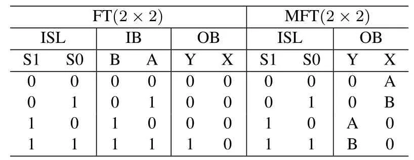
The functional table(FT)and modified(optimized)functional table(MFT)of the proposed 2×2 size data path selector cum router are shown in Table 1.Here input select lines(ISL)are S1,S0;the incoming bits(IB)are B,A;and the output bits(OB)are Y,X.The MFT is the simplified functional table,and it shows how the incoming data is passing through output lines.To understand the workings of the proposed 2×2 data-path selector cum router,it is easy to use the MFT.From the transmitted data bits,one can straightforwardly derive the Boolean expressions of the two output lines of 2×2 block as shown in equations(1)and(2),respectively.
To realize the design straightforwardly,we added a signal flow diagram(SFD),as shown in Figure 7.The input select line is S0,and the output path selector is S1,according to the SFD in Figure 7.The majority gate-based schematic of the proposed 2×2 block is shown in Figure 8.The proposed QCA layout is shown in Figure 9(a).It has been employed using the popular tool QCADesigner 2.0.1[19].The simulation output in normal form and bus form is shown in Figure 9(b) and Figure 9(c),respectively.The outcome has been generated using 10 clocking zones or clock phases in the QCA layout designing tool; therefore,the latency or input-output delay is 2.5 clock cycles.It is worth mentioning that 4 clock zones or 4 clock phases are equal to 1 clock cycle.The proposed QCA layout is a single-layer design which is an essential feature of this design.The entire layout has been developed using 55 QCA cells;hence the cell complexity or cell count is 55.The total area(cell area)occupied by this circuit is 0.13µm2(0.01782µm2); therefore,the area usage is 13.70%.The simplicity,less area requirement,and fewer cell count or lower complexity are the striking features of the proposed 2×2 data path selector cum router.
3.2 QCA Implementation of(4×4)Block
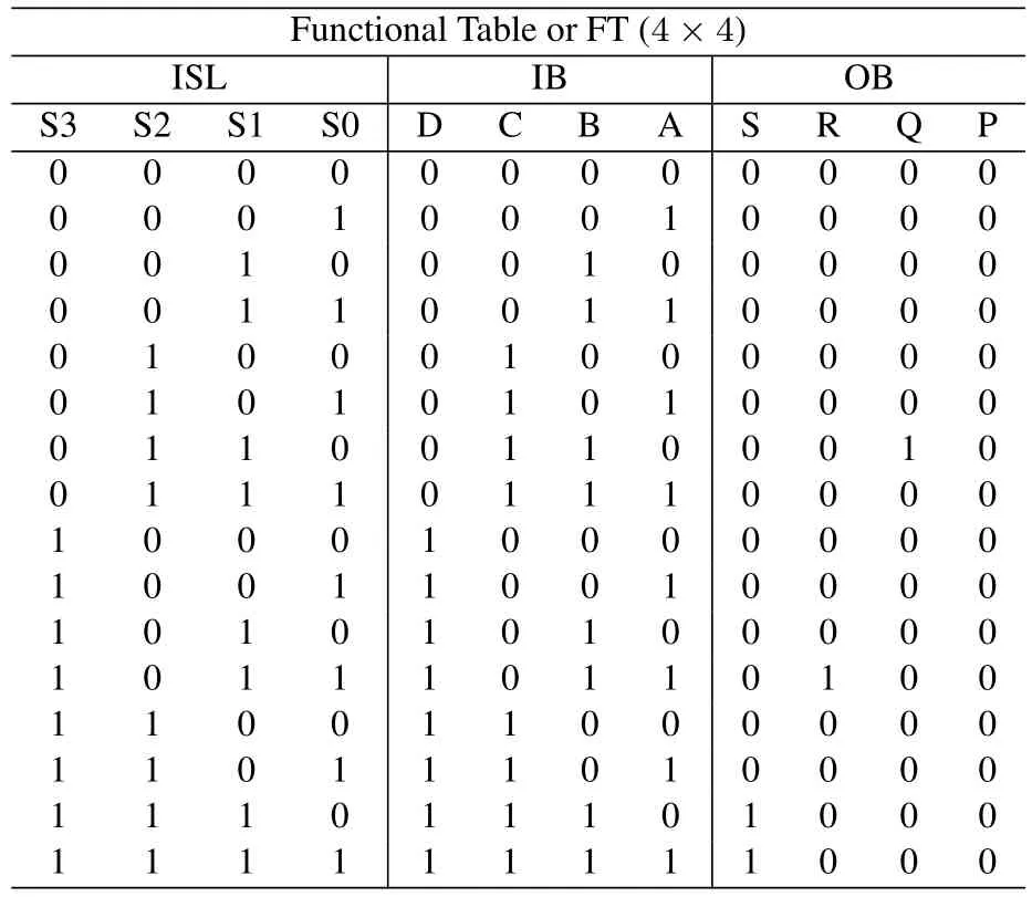
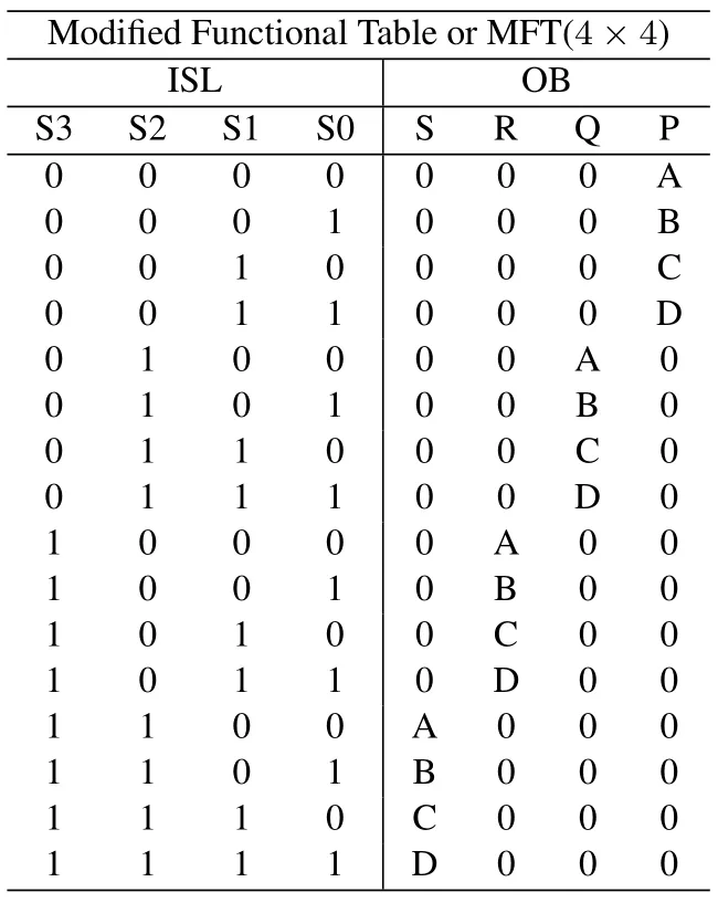
The extended design of the data path selector cum router with size 4×4 has been carried out successfully.Here the implementation method is the same as the previous unit (2×2) implementation procedure.The functional table or FT (4×4) is shown in Table 2,where the input select lines (ISL) are S3,S2,S1,and S0;the incoming bits are D,C,B,and A;the output bits are S,R,Q,and P.The simplified or modified functional table(MFT)is shown in Table 3,which may help to understand the working of 4×4 size data path selector cum router easily and quickly.

Table 1.Functional table (FT) and modified functional table(MFT)of proposed 2×2 block.
The majority gate or majority voter-based schematic of the proposed 4×4 size data path selector cum router is shown in Figure 10.The proposed QCA layout is shown in Figure 11 (a),designed using the tool QCADesigner.The simulation output in standard form and bus form is shown in Figure 11(b)and Figure 11(c),respectively.Like the previous design(2×2 size),here also(4×4 size),the output has been generated after using 10 clocking zones or clock phases in QCA technology; therefore,the latency or inputoutput delay is 2.5 clock cycles.Again,it is a singlelayer design which is the most significant feature of this design.In this design,the cell complexity or cell count is 134,the total occupied area is 0.34µm2,the cell area requirement is 0.049896µm2,and therefore the area usage is 14.67%.
IV.ENERGY ESTIMATION
The estimation of energy dissipation is an integral part of QCA based circuit analysis.Two popular power estimation tools,QCAPro [20]and QCADesigner-E or QDE[21],have been used to calculate the energy dissipation of the proposed data path selector cum router.
4.1 Energy Estimation Using QCAPro Tool
QCAPro is a popular tool to estimate the non-adiabatic power loss of QCA circuits during switching operations for different tunneling energy levels at a fixed temperature.The power dissipation of a QCA circuit is calculated with the help of the Hartree-Fock approximation [20].During this process,the overall energy of a QCA cell is calculated using the following Hamiltonian matrix as mentioned in equation(3).
Here H is a 2×2 Hamiltonian matrix,Ciindicates the polarization of the ith adjacent cell,fi,jis the geometrical factor related to electrostatic interaction between theithcell andjthcell,γis tunneling energy between two cell states,andEKis the kink energy of two neighboring cells having opposite polarization[20,22].
For every clock cycle,the expectation energy value of the cell is derived from the equation(4)below.
Whereis the coherence vector,ℏ is the reduced Planck’s constant,andis the energy vector (threedimensional)[20,23].
QCAPro is a suitable energy estimation tool only for small and single-layered QCA circuits.Therefore,the proposed circuits are best suitable for energy analysis using QCAPro.The energy estimation has been carried out at a fixed temperature 2K with three different tunneling levels (γ=0.5EK,γ=1.0EK,andγ=1.5EK).Atγ=0.5EK,γ=1.0EK,andγ=1.5EK,the leakage energy dissipation of the proposed 2×2(4×4)data path selector cum router is 12.05meV(36.82meV),33.73meV(101.86meV),and 58.64meV(176.59meV); the switching power dissipation is 43.82meV(132.13meV),37.72meV(113.83meV),and 32.34meV(94.69meV);the total power dissipation is 55.87meV(168.95meV),71.45meV(215.69meV),and 89.98meV(217.28meV).Table 4 shows the detailed energy dissipation data of the proposed QCA circuits at a temperature of 2 K.As expected,the proposed 2×2 block dissipates∼89%,∼88%,and∼88%less energy atγ=0.5EK,γ=1.0EK,andγ=1.5EK,respectively,concerning the prior design[12].Similarly,the proposed 4×4 block dissipates∼21 times,∼21 times,and∼21 times less energy atγ=0.5EK,γ=1.0EK,andγ=1.5EK,respectively,compared to the existing design[13].

Table 2.Functional table(FT)of proposed 4×4 block.
4.2 Energy Estimation Using QDE Tool
QCADesigner-E or QDE [21]is a new tool to estimate the energy dissipation of QCA circuits.In this energy estimation approach,a cell is considered a bath of energy,which is the mathematical summation of all possible energy transfers during circuit operation.It is denoted as,also known as,in which the energy is going to the environment from the cell.Mainly there are three parts of the total energy dissipation of QCA circuit; first partor,the second part of energy dissi-pation is the energy transfer between cells and clock,denoted as; and the last part of energy dissipation only the part of input-output energy sharing between cells and represents as.is the difference between the incoming energy part to the outgoing energy part,written as==.During this energy estimation process an error may be generated as positive or negative of magnitude,=(+) [24].A negative error indicates that the energy is coming towards QCA cells [21].It should be noted that a cell of a circuit is assigned fixed coordinates,and the entire circuit is represented as an array of cells during this process [21,24].Total energy dissipation of the proposed 2×2 (4×4) module is 18.60meV(64.60meV) with a negligible error of−1.71meV(−6.11meV)and average energy dissipation per cycle is 1.69meV(5.87meV)with an insignificant error of−0.0156meV(−0.555meV).All energy dissipation values are tabulated in a nutshell in Table 5.In particular,the proposed 2×2 size circuit and 4×4 size circuit dissipates∼86%and∼60%less energy compared with the best prior reported design[12]and[13],respectively.

Table 3.Modified functional table(FT)of proposed 4×4 block.
V.COMPARISON
For evaluating our proposed designs,several parameters for comparison are given in Table 6.It shows the design summary of the proposed 22 and 4×4 data path selector cum router,including prior reported similar designs.The comparing parameter includes the cell complexity,cell area requirement,total occupied area,area usage,latency,energy dissipation,etc.

Table 4.Energy dissipation analysis of the proposed and prior designs using QCAPro at temperature 2K.

Table 5.Energy dissipation analysis of the proposed and prior designs using QCADesigner-E(QDE).

Table 6.Comparative study of the proposed and prior designs.
Compared with previous designs,the proposed 2×2 and 4×4 data path selector cum routers have a smaller cell complexity (cell count),less occupied area,and lower latency that is obvious in Table 6.In particular,the proposed 2×2 unit requires∼86% fewer cells; therefore,there are∼7 times improvements in cell complexity compared with the best existing design[12].Moreover,the proposed 2×2 block occupies∼85% less requirement of cell area and∼87% less total occupied area than the previous design in [12].In addition,the proposed block has∼13.70% area usage,which is quite good,and the design is a single layer design,which is very important for QCA layout design.Furthermore,compared with the existing design[12],there is∼64%improvement in latency for the proposed 2×2 design.In the case of energy dissipation,there is a notable improvement in the proposed 2×2 design.At 2Ktemperature,there is∼9 times improvement in energy dissipation when tested in the QCAPro tool atγ=0.5EK.In addition,the proposed 2×2 circuit dissipates∼86% less energy if the experiment is performed in QDE tool.
According to Table 6,the proposed 4×4 block requires 63%fewer cells;therefore,cell complexity improves∼3 times compared with the design reported in [8].There is∼63% and∼37 improvements in cell area and total area requirement,respectively,compared to the design in [8].Furthermore,the area usage of the proposed 4×4 block is∼15% which is good,and it is a single layer design which is one of the most important advantages.In 4×4 unit,the latency improves∼17% compared to [8].Compared to the design reported in[13],there are∼21 times(atγ=0.5EK)and∼60%improvements in total energy dissipation of the proposed 4×4 circuit when experiment performed in QCAPro and QDE,respectively.
VI.CONCLUSION AND FUTURE DIRECTION
A simple and efficient 2×2 QCA based data path selector cum router has been reported in this article.Then the work has been extended to implement 4×4 module.To design the proposed circuits,we have used few simple multiplexers (MUX) and demultiplexers(DeMUX).By utilizing these simple MUX and De-MUX units,the proposed designs attained a significant improvement in terms of cell complexity (cell count)and covered area over the existing designs.In particular,the proposed 2×2 (4×4) block exhibits 86%(63%) lower cell complexity and 87% (37%) smaller area requirement than the prior reported similar designs.In addition,the simplicity of the proposed architecture and the single-layer QCA layout helps to make the proposed work more significant and attractive to QCA researchers.The proposed designs also achieved a notable improvement in terms of energy dissipation.The proposed 2×2(4×4)block showed 86%(60%)lower energy dissipation when examined by the tool QCADesigner-E (QDE),which demonstrates the advantage of the designs.We anticipate that the proposed simple blocks will be a reference model for designing higher-order QCA based data path selector cum router and similar designs in the nanocommunication paradigm.
- China Communications的其它文章
- Environment Information-Based Channel Prediction Method Assisted by Graph Neural Network
- Multi-Scenario Millimeter Wave Wireless Channel Measurements and Sparsity Analysis
- AG Channel Measurements and Characteristics Analysis in Hilly Scenarios for 6G UAV Communications
- Long-Range VNA-Based Channel Sounder: Design and Measurement Validation at MmWave and Sub-THz Frequency Bands
- A Novel Millimeter-Wave Channel Measurement Platform for 6G Intelligent Railway Scenarios
- A Geometry-Based Stochastic Scattering Channel Model for V2V Communications in Dense Urban Street Environments

