
A mini review:Constructing perovskite p-n homojunction solar cells
2022-06-20 06:19YananSunWeiChenZhengyiSun
Chinese Chemical Letters 2022年4期
Yanan Sun,Wei Chen,Zhengyi Sun
Key Laboratory of Flexible Electronics(KLOFE),Institute of Advanced Materials(IAM),Nanjing Tech University,Nanjing 211816,China
ABSTRACT Organic metal halide perovskite materials have excellent photoelectric properties,and the power conversion efficiency(PCE)of the perovskite solar cells(PSCs)has increased from 3.8% to more than 25%.In the development of PSCs,innovative architectures were being proposed constantly.However,the use of the electron transport layer(ETL)and hole transport layer(HTL)increases manufacturing costs and process complexity.Perovskite material has ambipolar charge transport characteristics,so it could functionalize as both the optical absorption layer and carrier transport layer(CTL).In this review,we analyzed the p/n-type perovskite materials,perovskite p-n homojunction solar cells,and carrier transport layers-free(CTLs-free)devices.Finally,we propose some innovative device architectures.We hope that this mini review could pave way for the simplification of the architectures,promote the preparation of the low-cost and high-efficiency devices,and accelerate the commercialization of the PSCs.
Keywords:Perovskite Ambipolar p-n Homojunction Solar cell
1.Introduction
Solar energy is inexhaustible and environmental-friendly.It could help mankind to solve the current energy and environmental challenges,as shown in Fig.1a.Organic metal halide perovskite is used as the light absorption layer in PSCs,as shown in Fig.1b.The general formula of perovskite is ABX3,where A represents a monovalent organic cation(such as CH3NH3+,CH(NH2)2+,Cs+,Rb+),B represents a bivalent metal ion(such as Pb2+,Sn2+,Ge2+),and X symbolizes a halide ion(such as Cl-,Br-or I-),as shown in Fig.1c[1,2].It has high absorption coefficient[3,4],low exciton binding energy[5-7],ambipolar characteristic[5,8,9],longdistance electron-hole diffusion[10,11],and high defect tolerance[12-14],and was used as the absorbing material in 2009[15].Then,with the help of device architecture engineering[16,17],film morphology engineering[18,19],energy level alignment[20,21],electron transport materials[22,23],hole transport materials[24],additive engineering[25,26],interface engineering[27],composition engineering[28],defect engineering[29],hysteresis optimization[30,31],stability optimization[26,32]etc.,the PCE of the device has risen from the initial 3.8% to higher than 25%[15,33]
In the development of PSCs,innovative architectures had been proposed constantly,as shown in Fig.2.PSCs had experienced the development from the liquid state to solid state.The solid-state devices could be divided into the mesoporous and planar architectures.The planar architectures could be divided into the regular(n-i-p)and reverse(p-i-n)architectures.Then,scientists and researchers further prepared the HTL-free and ETL-free PSCs.Table 1[4,15,34-53]summarized the evolution of the architectures and PCEs for the devices.
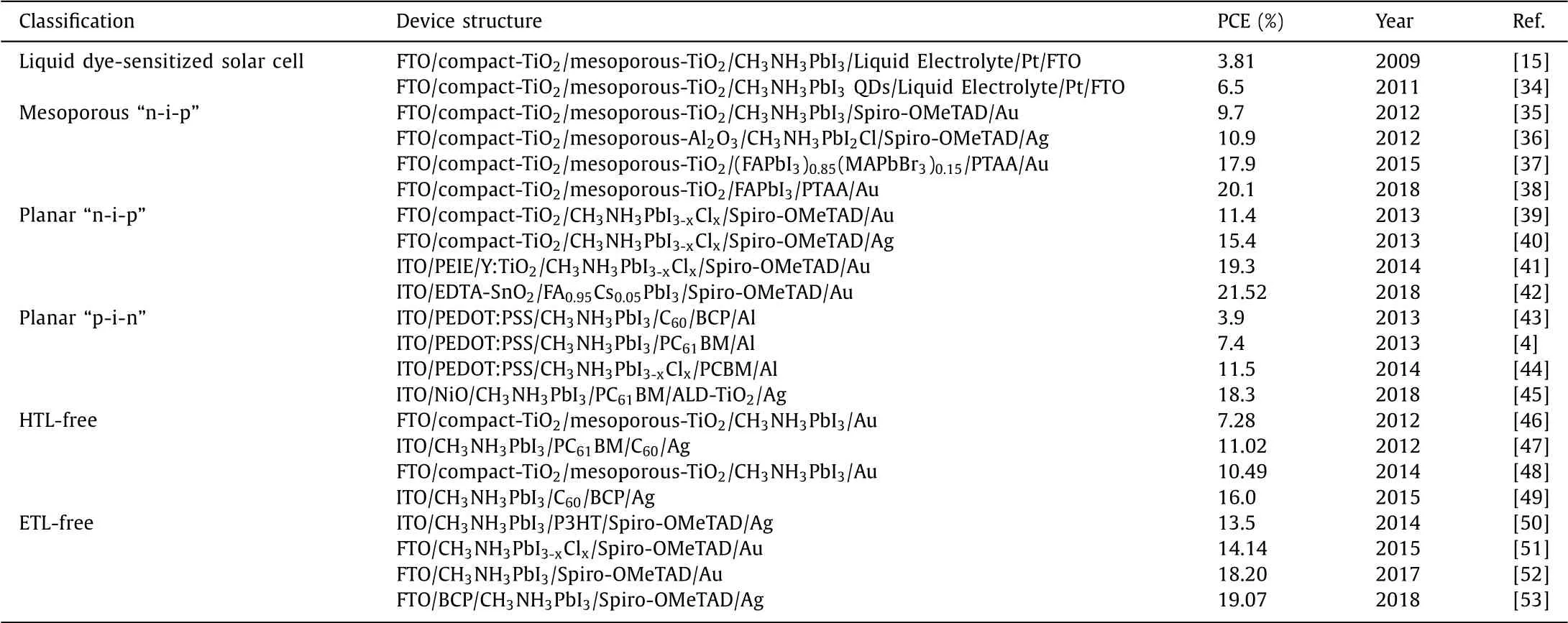
Table 1 Evolution of the architectures and the PCEs of PSCs.
Generally,the PSCs contain a HTL and an ETL to build in the electric field,which can suppress the recombination of electrons and holes and promote their separation.However,the use of ETL and HTL increased the manufacturing costs and process complexity.Organic metal halide perovskite had ambipolar carrier transport characteristics,so it could be used as the absorption layer and CTLs simultaneously.But the recombination probability of the electrons and holes was increased significantly and the performance of the device was poor.The establishment of the perovskite p-n homojunction could enhance the built-in potential and improve the performance,but there was few research on this aspect[17,54].
Herein,we analyzed the p/n-type perovskite materials,perovskite p-n homojunction solar cells,and CTLs-free PSCs.Finally,we proposed some innovative architectures.We hoped that this mini review could provide reference for the simplification of PSCs,pave way for the preparation of low-cost and high-efficiency devices,and accelerate the commercialization process.
2.Perovskite p-n junction
The first solar cell was invented in 1954.It was a silicon(Si)solar cell based on p-n junction,as shown in Fig.3.Due to the huge difference of electron concentration between n-type and ptype Si,the electrons would diffuse from the n-type Si to p-type Si and holes would diffuse from the p-type Si to n-type Si.When the diffusion force and electric field force reached equilibrium,an internal electric field would be formed within a certain thickness on both sides at the interface.
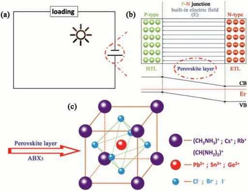
Fig.1.(a)Circuit diagram of the PSCs.(b)p-n junction in device.(c)lattice structure of the ABX3-type perovskite.
When the p-n junction was illuminated,a half of photogenerated carriers were produced in the form of excitons and the other were free electrons and holes.Under the function of built-in potential,the majority of excitons would be dissociated into the free electrons and holes.The electrons would be transferred to n-type Si and then extracted by the cathode,while the holes would be transferred to p-type Si and then extracted by the anode.
2.1.Perovskite as hole transport layer
In the HTL-free PSCs,perovskite layer should have high hole concentration and a certain hole mobility to ensure the transport and extraction of the holes.Because the ionic radius of boron tetrafluoride(BF-4,0.218 nm)was similar to iodine(I¯,0.220 nm),Chenet al.prepared the MAPbI3-x(BF4)xpolycrystalline films by adding MABF4into the perovskite precursor solution.The result showed that the hole mobility was improved significantly and the films behaved as a good p-type semiconductor.In the device,perovskite layer not only acted as the light absorption layer,but also the HTL[55].Aharonet al.prepared the HTL-free PSCs by twostep solution process.The perovskite layer was MAPbI3,FAPbI3,or FA1-xMAxPbI3.Through the surface photovoltage spectrum(SPS)analysis,they were all p-type semiconductors[56].Etgar and Labanet al.also used MAPbI3as both the absorption layer and HTL in HTL-free PSCs.The PCE was 7.28% and 8%,respectively[46,57].Leeet al.prepared the Cs2SnI6film by solution method and employed it as the HTL in solid dye-sensitized solar cells[58].Table 2[46,47,55-70]summarized the architectures and the PCEs of the devices,in which perovskite layers were used as the HTLs.
Table 2 PSCs using perovskites as the HTLs.
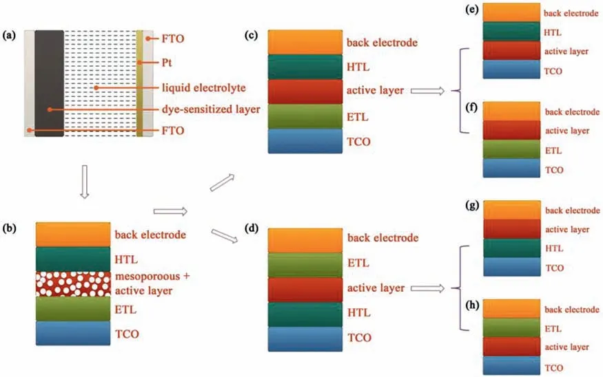
Fig.2.Development of the architectures:(a)liquid dye-sensitized solar cell;(b)mesoporous“n-i-p”;(c)planar“n-i-p”;(d)planar“p-i-n”;(e)planar“n-i-p”-ETL free;(f)planar“n-i-p”-HTL free;(g)planar“p-i-n”-ETL free;(h)planar“p-i-n”-HTL free.
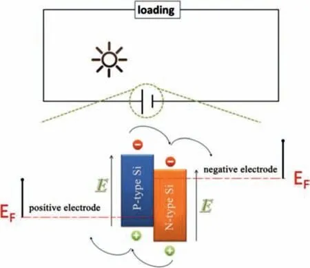
Fig.3.Si solar cell based on p-n junction.
2.2.Perovskite as electron transport layer
Normally,the devices had no selectivity for electrons and holes in the ETL-free PSCs.The serious carrier recombination would occur at the interface between the perovskite and the cathode.Cuiet al.modulated the semiconductor type of the film by controlling the annealing temperature.When the temperature was increased from room temperature to 150 °C,the semiconductor was converted from p-type to n-type.The p-n junction was composed of an n-type perovskite layer and a p-type hole transport layer.And the p-n junction improved the directional transport ability and reduced the recombination probability for electrons and holes.Finally,the PCE of the ETL-free PSCs could reach 15.69%[71].The semiconductor type of film was closely related to the precursor composition,processing conditions,and preparation methods(such as evaporation,solution).And it could be modulated from n-type to p-type,or vice versa correspondingly.Wanget al.found that the semiconductor type was essentially determined by the intrinsic defects in films.The composition of perovskite precursors and annealing temperature could affect the intrinsic defects.Theoretical analysis showed the relative size of formation energy for the intrinsic defects in MAPbI3films:VPb2+<VI-<Pb2+i<VMA+.In the system of PbI2-rich or MAI-deficient,there was a tendency to formVI-,rather than Pb2+iorVMA+.And the film tended to behave as the n-type semiconductor.However,in the system of MAIrich or PbI2-deficient,there was a tendency to formVPb2+rather thanVI-.And the film tended to exhibit a p-type feature[72].By adding antimony chloride(SbCl3)into the precursor solution of MAPbI3-xClx,Huanget al.introduced Sb3+into the crystal structure of perovskite,which made the MAPb1-ySbyI3-xClxfilm behave as an n-type semiconductor.The X-ray diffraction(XRD)patterns showed that the introduction of Sb3+did not change the lattice structure of MAPbI3-xClx.In addition,the optical absorption spectra showed that the band gap did not change significantly.The Hall effect measurement showed that the electron concentration in MAPbI3-xClxfilm was about 7.2 × 1014cm-3when the doping concentration was 0.But when the doping concentration was 2%,the electron concentration in MAPb1-ySbyI3-xClxfilm was increased to 8.3 × 1016cm-3and the conductivity reached 2.19 × 10⁻⁶Ω-1cm-1.In the device,perovskite layer was used as both the absorption layer and ETL.The p-n junction was constructed between the doped n-type perovskite film and p-type HTL.Accordingly,the PCE was increased from 7.71% to 12.62%[73].Graphite materials were abundant,cheap,environmentally friendly,and stable and they could extract holes and block electrons.Weiet al.constructed the p-n junction between the perovskite layer and graphite electrode.By optimizing the interface contact,the PCE of the device increased from 2.60% to 11.02%[74].Table 3[50-53,71,73,75-86]showed the architectures and the corresponding PCEs,in which perovskites were used as the ETLs.
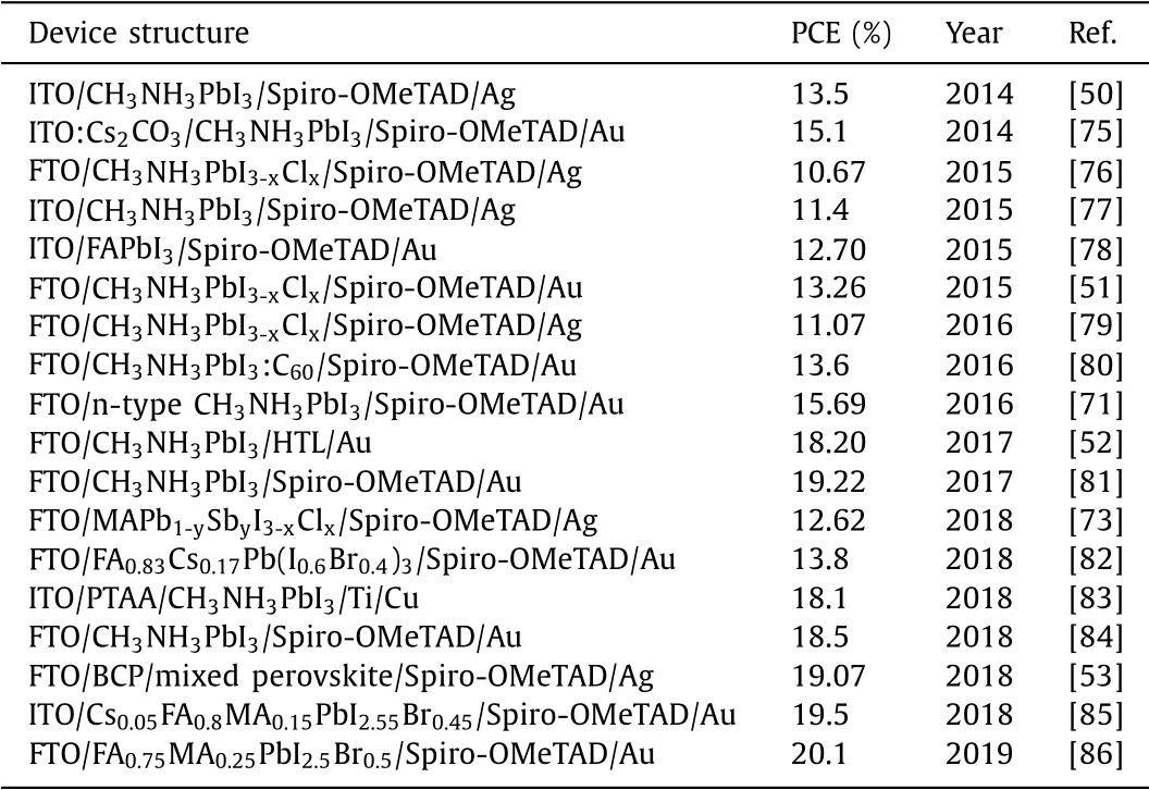
Table 3 PSCs using perovskites as the ETLs.
2.3.Perovskite p-n homojunction solar cells
The underlying physical principles in p-n junction had been studied for decades and most photovoltaic devices based on conventional inorganic semiconductors(such as GaAs,CIGS,and CdTe)were invented.Because the perovskite possessed ambipolar carrier transport characteristics,it could be used as the CTL.Some research teams had prepared the perovskite p-n homojunction solar cells.
The first layer of perovskite could be prepared by solution method.However,the second layer could not be prepared by solution method,otherwise the first layer would be destroyed.The perovskite films could also be prepared by the double source evaporation system[40].By controlling the evaporation rate of MAI and PbI2,the p-type and n-type perovskite films could be deposited sequentially.Finally,the perovskite p-n homojunction was constructed.Due to the establishment of the built-in electric field,the carrier recombination rate was reduced significantly and the directional carrier transport was enhanced.Accordingly,the PCE was increased to 14.7%[87].Cuiet al.had prepared the n-type and p-type MAPbI3films by controlling the stoichiometric ratio of precursors.By constructing the perovskite p-n homojunction,the PCE was increased from 17.76% to 20.80%.Their work demonstrated that constructing perovskite p-n homojunction could be a valid alternative to enhance the performance of the device[88].Ouet al.prepared the n-type perovskite film with a certain thickness.Then,the MoO3was introduced into the surface of the film,which converted the n-type film with a thickness of 20 nm into p-type.The built-in potential and depletion width were 0.5 eV and 10 μm,respectively[89].Sunet al.prepared the n-type(FA,MA)Pb(Cl,Br,I)3and p-type FAPb1-xSnxI3films sequentially in the device and the corresponding PCE could reach 21.4%[90].Chenet al.spun the guanidine bromide(GABr)isopropanol solution on the surface of perovskite film,followed to form a certain layer of n-type GAxFA0.8Cs0.2Pb(I0.7Br0.3+x/3)3at the perovskite/C60interface by annealing.The PCE of the device was increased from 17.16% to 18.19%[91].Renet al.prepared the p-type perovskite films by controlling the stoichiometric ratio of precursors.Then,an n-type perovskite layer with a certain thickness was achieved on the surface by Ar+bombardment.Finally,a perovskite p-n homojunction was constructed successfully[92].Xiaoet al.showed that the applied electric field could make point defects migrate in films and cause the aggregation on the surface,as shown in Fig.4.The aggregation could produce the n-type and p-type doping[93].
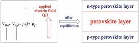
Fig.4.The n-type and p-type doping in perovskite by external electric field.
The double layers(MAPbI3/MAPbIxBr3-x)was formed by coating the amines bromide(MABr)solution on the top of MAPbI3.The double layers promoted the hole extraction and reduced the recombination probability.Finally,the PCE could reach 16.2%[94].Table 4[74,87-92,94,95]summarized the architectures and the PCEs of the perovskite p-n homojunction solar cells.
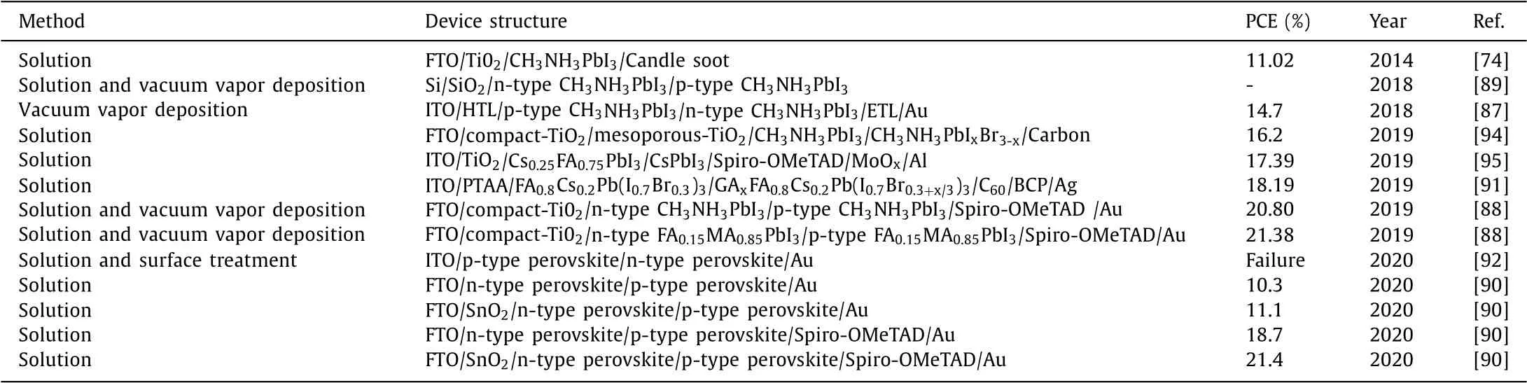
Table 4 The perovskite p-n homojunction solar cells.
In a word,the perovskite p-n homojunction could enhance the built-in electric field.The built-in electric field could suppress the recombination of electrons and holes and make the electrons and holes migrate to the cathode and anode side in the opposite direction.For the PSCs with ETL and HTL,constructing perovskite p-n homojunction could further improve the performance of the device.Regard to CTL-free PSCs,the perovskite p-n homojunction could be used to simplify the architecture and ensure the PCE simultaneously.
2.4.Conclusion
Based on the above analysis,we took the MAPbI3as an example to summarize the preparation of p-type and n-type perovskite films and analyze the internal mechanism.These methods for modulating the majority carrier type in perovskite could pave way for the fabrication and investigation of the perovskite p-n homojunction solar cells.
(I)The electronic conductivity of the perovskite film could be tuned by changing the molar ratio of the precursors(PbI2/MAI).When PbI2/MAI>1,the film tended to behave as an n-type semiconductor.When PbI2/MAI<1,the film tended to behave as a p-type semiconductor.
(II)Heterovalent doping could modulate the majority carrier type in perovskite.The introduction of monovalent ions(such as Ag+,Na+,K+,and Rb+)could make the film behave as a p-type semiconductor,while the introduction of trivalent ions(such as Sb3+and Bi3+)could make the film behave as an n-type semiconductor.
(III)Annealing temperature and time could also affect the semiconductor type of the perovskite.High temperature(100-150 °C)and long-term annealing treatment could make the film behave as an n-type semiconductor,while low temperature(<100 °C)and short-term annealing treatment could make the film behave as a p-type semiconductor.
The molar ratio of the precursors,heterovalent doping,and annealing process could affect the defect type(VPb2+,VI-,Pb2+i,andVMA+)in perovskite.The majority carrier type was closely related to the defects,and could be reflected by the position of Fermi level(EF).We reproduced the schematic energy level diagram of some perovskite films including the position ofEF,as shown in Fig.5[71-73,88,96-99].
3.Devices without any carrier transport layer(CTLs-free)
The ambipolar characteristic of the perovskite materials endowed them with great potential to construct the CTLs-free PSCs.The photo-induced excitons could be dissociated into free electronsand holes in the absence of the CTLs owning to the low binding energy.Long carrier diffusion length and high carrier mobility allowed the carriers to pass through the perovskite layer and be extracted by the electrodes.The preparations of a continuous,compact,smooth,and flat perovskite film,suitable energy level,and a p-n junction inside the device were imperative to a high efficiency CTLs-free PSCs.
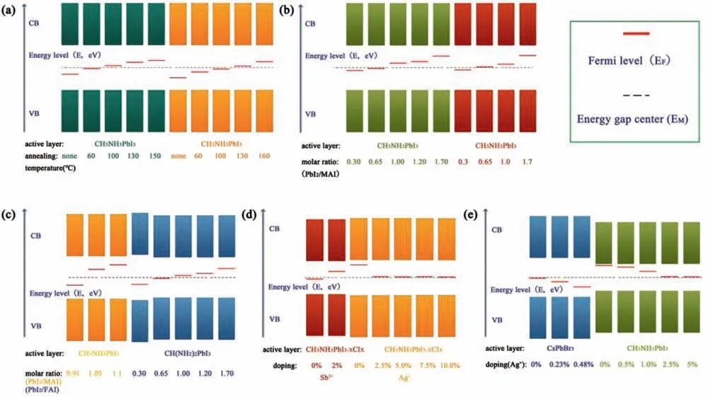
Fig.5.(a)Influence of the annealing temperature(0-160 °C)[71,96].(b)Influence of the molar ratio for the precursors[72,97].(c)Influence of the molar ratio for the precursors[88,97].(d)Influence of the heterovalent ion doping[73,98].(e)Influence of the heterovalent ion doping[98,99].
The perovskite p-n homojunction,containing a p-type FAPb1-xSnxI3layer and an n-type(FA,MA)Pb(Cl,Br,I)3layer,was prepared in a CTLs-free PSCs.The PCE could reach 10.3%[90].By controlling the molar ratio of the perovskite precursors,Cuiet al.prepared an n-type and a p-type films sequentially.In the device,the perovskite films were used as both the absorption layer and the CTLs.The corresponding PCE could reach 8.08%[88].Theoretical calculation showed that the CsSnI3had a direct band gap of 1.3 eV.At room temperature(300 K),it behaved as a p-type semiconductor with an exciton binding energy of 18 meV[100].Chenet al.prepared the CTLs-free PSCs by using CsSnI3as the absorption layer.However,the PCE was only 0.9%[101].Duanet al.had prepared the CTLs-free PSCs by employing CsPbBr3and carbon materials as the absorption layer and electrode.The initial PCE was only 2.35%.But the PCE could be increased to 4.10% after the interface optimization[102].Table 5 summarized the architectures and PCEs of the CTLs-free PSCs.
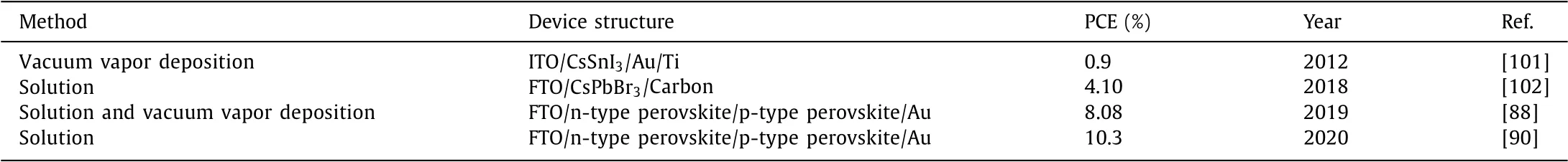
Table 5 Devices of the CTLs-free PSCs.
4.Summary and outlook
In summary,we analyzed the p/n-type perovskite materials,perovskite p-n homojunction solar cells,and CTLs-free PSCs.In order to construct the CTLs-free perovskite p-n homojunction solar cells,we could learn the preparation methods of p-type and Ntype perovskite films from the different studies.It should be noted that the electrode layers would directly contact with the perovskite layers.And the contact quality was generally poor.In order to optimize the interfaces,we could refer to the methods in the CTLs-free PSCs.
Carbon materials had an ability of extracting holes from the perovskite layer and their properties could be adjusted by con-trolling the doping level and the preparation process.In addition,transparent conductive oxide(TCO)played a role of transmitting sunlight and extracting carriers in PSCs.And its semiconductor type could also be changed by doping.If the N-type or p-type TCO could be used as both the CTL and electrode,the architecture of the device could be further simplified.In view of this,we proposed some innovative architectures,as shown in Fig.6.
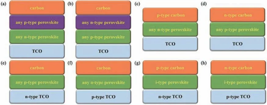
Fig.6.Some innovative architectures of the PSCs.
In the future,employing carbon materials and TCO as the electrode and CTL,using perovskite materials as the absorption layer,and constructing the p-n junction in device were expected to simplify the architecture and ensure the PCE of the device simultaneously.We hoped that this mini review could pave way for the simplification of the architectures,promote the preparation of lowcost and high-efficiency devices,and accelerate the commercialization of the PSCs.
Declaration of competing interest
The authors declare no conflict of interest.
Acknowledgment
The authors gratefully acknowledge the financial support from the Natural Science Foundation of Jiangsu Province(No.BK20191358).
 Chinese Chemical Letters2022年4期
- Chinese Chemical Letters的其它文章
- Key progresses of MOE key laboratory of macromolecular synthesis and functionalization in 2020
- Small nanoparticles bring big prospect:The synthesis,modification,photoluminescence and sensing applications of carbon dots
- Cell membrane-coated nanoparticles for immunotherapy
- Diketopyrrolopyrrole-derived organic small molecular dyes for tumor phototheranostics
- Exosome based miRNA delivery strategy for disease treatment
- Recent advances in targeted stimuli-responsive nano-based drug delivery systems combating atherosclerosis