
Strain tuned efficient heterostructure photoelectrodes
2022-06-18 10:53HihongZhengMingyngLiJinsongChenAnhngQunKihngYeHngRenShengHuYngCo
Chinese Chemical Letters 2022年3期
Hihong Zheng,Mingyng Li,Jinsong Chen,Anhng Qun,Kihng Ye,Hng Ren,Sheng Hu,d,Yng Co,d,∗
a State Key Laboratory of Physical Chemistry of Solid Surfaces,Collaborative Innovation Center of Chemistry for Energy Materials (iChEM),College of Chemistry and Chemical Engineering,Xiamen University,Xiamen 361005,China
b Department of Chemistry,University of Texas at Austin,Austin,TX 78712,United States
c Guangzhou Key Laboratory of Clean Transportation Energy Chemistry,School of Chemical Engineering and Light Industry,Guangdong University of Technology,Guangzhou 510006,China
d Pen-Tung Sah Institute of Micro-Nano Science and Technology,Xiamen University,Xiamen 361005,China
Keywords:Photoelectrochemical water splitting van der Waals heterostructures Two-dimensional MoS2 Strain engineering Scanning electrochemical cell microscopy
ABSTRACT van der Waals (vdWs) heterostructures based on two-dimensional (2D) materials have become a promising candidate for photoelectrochemical (PEC) catalyst not only because of the freedom in materials design that enable the band-offset construction and facilitate the charge separation.They also provide a platform for the study of various of interface effect in PEC.Here,we report a new kind of mixed-dimensional vdWs heterostructure photoelectrode and investigate the strain enhanced PEC performance at vdWs interfaces.Our heterostructures are composed of 2D n-type MoS2 nanosheets and three-dimensional (3D) p-type Cu2O nanorod arrays (NRAs),where Cu2O NRAs introduce periodically strain in the p-n junction interface.We find a promotion of the HER catalytic activities in heterostructure based PEC photoelectrodes using in-situ measurement techniques including the scanning electrochemical cell microscopy and various local spectrum probe measurements.This is attributed to the efficient charge separation at the strained heterointerface.Our results demonstrate an interesting venue for understanding the local interface effects with high spatial resolution,and shed light on design and developing high-efficiency photoelectrodes.1L MoS2/Cu2O vdWs heterostructure photocathodes were prepared by nanoindentation technology.The effects of strain on promoting charge separation at the heterointerface were verified by the enhanced performances in PEC hydrogen evolution reaction of vdWs heterostructure through scanning electrochemical cell microscopy technique and various local spectrum probe measurements.
Hydrogen production by photoelectrochemical (PEC) water splitting converts the inexhaustible solar irradiation to storable H2as clean energy,and thus has received widespread attention [1–4].One of the key limiting factors for the PEC performance is the fast recombination of photo-generated charge carriers.Among various strategies for enhancing charge separation efficiency,the creation of heterojunctions by assembling two distinct materials has been demonstrated to be promising.It allows for efficient electron-hole separation where charge carriers generated in one photocatalytic material is able to transfer through the contact interface to the other material [5–9].In particular,van der Waals(vdWs) heterostructures constructedviathe vdWs interaction between dangling-bond-free materials have attracted much attention for a number of reasons: First,vdWs interactions allow creating artificial heterostructures with sharp and atomically clean interfaces[10].These characteristics provide them as ideal model systems to study the interface effect for PEC.The unique properties of 2D materials like their high specific surface area,proper crystal facet,and large number of active sites will further improve the PEC performance [11,12].Second,the heterostructure construction requires only physical assembly of two kinds of materials regardless of their lattice structures and dimensions [13,14].This allows considerable freedom in integrating,for example two-dimensional (2D) materials,with materials with different dimensions,and enables the creation of naturally non-existing heterostructures containing merits from each of their components [15–19].Moreover,the 2D materials based vdWs heterojunction allows a short photo-generated charge diffusion distance,and further accelerates charge separation to improve the PEC performance [20,21].This is different from the traditional two-dimensional (2D) materials,such as graphene and black phosphorus where the charge separation is limited by the in-plane diffusion [22–24].
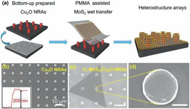
Fig.1.(a) Scheme of the fabrication process of 1L MoS2/Cu2O (NRAs) heterostructure nanorod arrays.SEM image of top surface view of (b) Cu2O nanorod arrays,the inset is the AFM height profile of the Cu2O NRAs.(c) 1L MoS2/Cu2O heterostructure nanorod arrays,and (d) an enlarged view of a single 1L MoS2/Cu2O heterostructure nanocolumn.Scale bar in (c): 10 μm.Scale bar in (d): 2 μm.
However,due to the lattice mismatching,strain is usually produced at the interface of vdWs heterostructure when assembling multiple 2D layers together [25,26].Although it has been reported that strain engineering effectively tunes both the band structures and band alignment in PEC anode and optimize the charge transfer dynamic in heterostructure [27–29],the effect of strain to PEC performance in vdWs heterostructure based photoelectrode remains elusive.From fundamental level point of view,strain is a local effect and its influence to hydrogen evolution reaction (HER)requires probe measurements with high spatial resolution [30–32].However,the currently prevailing electrochemical detection for the current-voltage characteristics within the whole photoelectrode fails to acquire those detailed signals at the heterostructure interface.
With this in mind,in this work,we combine the scanning electrochemical cell microscopy (SECCM) technique and various local spectrum probe measurements to investigate the charge transfer at the strained PEC photocathode.The cathodes used here are made from mixed-dimensional vdWs heterostructure with 2D monolayered (1L) MoS2nanosheets and three-dimensional (3D) Cu2O nanorod arrays (NRAs).Here we choose 1L MoS2due to its high HER activities among 2D materials,and Cu2O as the traditional ptype semiconductor photocatalyst [11,12,33,34].Both of the materials have been reported for high HER catalytic activities.The unique feature detailed herein is the integration of the p-type Cu2O and ntype MoS2not only form a p-n junction for charge separation,but also Cu2O NRAs provide an essential nanopatterned structure for constructing MoS2/Cu2O heterostructure arrays with periodically strain-engineered interfaces.In this model system,we found the strain tuned heterostructures dramatically suppress the photoluminescence emission for 1L MoS2,indicating the enhanced charge separation at the heterostructure interface.As a result,both SECCMin-situmapping and PEC measurements demonstrate a promotion of the HER catalytic activities compared to photocathodes based on the pristine Cu2O,MoS2,and MoS2/Cu2O heterostructures without strain.

Fig.2.(a) Schematic diagram of strain distribution for 1L MoS2 in different regions of Cu2O NRAs substrate.(b) Raman spectra of 1L MoS2 at different regions.(c) Schematic diagram of 1L MoS2 on the single Cu2O nanorod.(d) Raman spectra of 1L MoS2 at different heights of Cu2O nanorod.
The periodically strained monolayer (1L) MoS2/Cu2O nanorodarrays (NRAs) mixed dimensional van der Waals (vdWs) heterostructures were prepared stepwise by the method depicted in Fig.1a and the “Experimental methods” section (Supporting information).First,the metallic Cu substrates were patterned by photo lithography and electron beam deposition (EBD) to form NRAs with diameters of ∼4 μm,∼100 nm to 200 nm in height,and intervals of 10 μm (Fig.1b).Then the patterned Cu NRAs were oxidized to Cu2O NRAs by anodizing,which were verified by Raman spectrum and X-ray photoelectron spectroscopy (XPS) (Figs.S1a and b in Supporting information).Second,the 1L MoS2prepared by chemical vaper deposition (CVD) method were transferred to the surface of Cu2O NRAs by polymer-assisted wet transfer processes(Fig.S2 in Supporting information for the optical image,Raman and photoluminescence (PL) characterization of the MoS2flakes)[35].Then the polymer was removed by acetone treatment.The scanning electron microscopy (SEM) images (Figs.1c and d),Raman scattering (Fig.S3a in Supporting information) and energy dispersive spectroscopy (EDS) mappings (see details in Figs.S3bg in Supporting information) of our samples suggest the successful fabrication of the 1L MoS2/Cu2O NRAs mixed dimensional vdWs heterostructure and intimate contact between the nanorods and flakes.
In order to investigate the distribution of strain on MoS2,the confocal Raman measurements were performed under the laser excitation of 532 nm.For the convenience of analyzing,we deliberately divide the 1L MoS2into two regions: the area A (on the flat Cu2O substrate) and the area B (on the top of the Cu2O NRAs),as shown in Fig.2a.It could be observed from Fig.2b that compared with the spectrum from area A,there is a red shift for the E12gpeak in the spectrum from area B.With the height of Cu2O nanorod increasing from 100 nm to 200 nm,the E12gpeak gradually redshifts,as shown in Figs.2c and d.This is attributed to the strain induced by the nanorods that modified the in-plane vibration mode of 1L MoS2and thus a shift of the corresponding E12gpeak [36,37].The position of the E12gpeak is directly related to the strain in MoS2samples and is calculated to be 0.2%,0.4% and 0.6% for 100 nm,150 nm and 200 nm nanorods,respectively,using the methods previously reported [37].The E12gpeak shift is only observed at area B,further confirming that the interfacial strain of 1L MoS2was originated from the Cu2O NRAs induced structure deformation.Note that the strain causes the changes in the restoring force constant of both the out-of-plane and in-plane vibration mode,resulting the red shifts of both E12gand A1gpeaks [37,38].
To spatiallyin-situinvestigate the PEC performance of the strained MoS2,a novel scanning electrochemical cell microscopy(SECCM) technique,in which the measured area on the samples could be confined in the scale of nano/micro-meters,was conducted on the 1L MoS2/Cu2O NRAs (see details in “Experimental methods” section in Supporting information).As shown in the schematic (Fig.3a),a single barrel nanopipette was filled with electrolyte solution (0.25 mmol/L KCl) and mounted on a zpiezoelectric positioner.The tip of the nanopipette probes were circle with the radii of approximately 250 nm.A bias of 0 Vvs.RHE,which would cause distinguished transient current upon the electrolyte at the pipet tip contacting the MoS2substrate,was applied between the quasi-reference counter electrode (QRCE) and the substrate.

Fig.3.(a) Diagram of SECCM measurement for 1L MoS2/Cu2O NRAs.(b) Linear sweep voltammetry of strain region at different height heterojunction.(c-e) SECCM photocurrent images of 1L MoS2/Cu2O NRAs with different heights.Scalar bar: 4 μm.
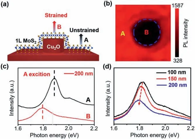
Fig.4.(a) Schematic diagram of strain distribution for 1L MoS2 in different regions of Cu2O NRAs substrate.(b) Scanning PL map with integrated peak intensity of the MoS2 on Cu2O NRAs.(c) PL spectra of 1L MoS2 at different regions.(d) PL spectra of 1L MoS2 at different heights of Cu2O nanorod.
The linear sweep voltammograms (LSVs) obtained from the strain regions (area B) show that under the illumination of 50 mW/cm2,the photo-current gradually increases by almost four times with increasing the height of Cu2O nanorod from 100 nm to 200 nm (Fig.3b).This photo-current dependence on nanorod heights was also observed in SECCM mappings as shownin Figs.3ce.Specially,by means of SECCM mapping,the HER activities of the heterostructures with or without strain can be compared in-situ.From Figs.3c-e,all the strained 1L MoS2/Cu2O NRAs heterostructures show a higher photo-current than the unstrained part,directly revealing the strain enhanced HER performance.
To study the mechanism of the enhanced PEC performance at the interface of 1L MoS2/Cu2O NRAs vdWs heterostructure,we performed a comprehensive PL measurement to reveal the charge transfer at the interface.As shown in Figs.4a and b,the PL intensities for the strained area B of the 1L MoS2/Cu2O NRAs vdWs heterostructures were almost 5 times lower than that for the unstrained area A,indicating a suppressed charge recombination at the heterostructure interfaces.We note that both the strain gradient and the band offset of p-n junction (in our case,1L MoS2/Cu2O heterostructure) could induce a build-in field [39].This field would adjust the carrier transfer at the interface,thus affecting the PL emission of 1L MoS2.To distinguish these two effects,we abrupt the MoS2-Cu2O interactions by depositing an insulating layer of 20 nm Al2O3on the surface of Cu2O NRAs,before the transfer of MoS2layers (Fig.S3a in Supporting information).Thus,only the strain in 1L MoS2would affect the PL signal.As shown in the PL intensity mapping of MoS2/Al2O3NRAs vdWs heterostructure (Fig.S3b in Supporting information),the built-in field induced by strain can dramatically enhance the PL intensity of 1L MoS2on the strain region,which is agreed with the previously reported funneling effects caused by the strain induced band-bending of MoS2[40–42].Thus,the effect of strain induced build-in field in MoS2layer could be excluded in our MoS2/Cu2O NRAs vdWs heterostructure from the opposite trend of the PL intensity.The decreased PL signal was mainly related to the suppressed charge recombination at the heterostructure interfaces.
Besides,as shown in the PL spectra for 1L MoS2/Cu2O NRAs vdWs heterostructure at regions with or without strain (Fig.4c),a red shift of A-exiton from 1.88 eV to 1.79 eV was observed for the strained area B with a 200 nm height Cu2O nanorod.And the red shift trend showed the height dependence of Cu2O nanorods(Fig.4d),indicating that the band gap of 1L MoS2decreases with the strain increases.The reduction of the optical band gap results from the biaxial tensile strain,which has been demonstrated in previous reports [43].These results indicated that the strain can effectively tune the band off-set and charge transfer at the interfaces of heterostructures,inducing a more efficient separation of photogenerated carriers,and thus exhibit an enhancement of HER activity.The strain induced charge separation is further proved by the enhanced photocurrent measured from the two-terminal phototransistor made by 1L MoS2/Cu2O NRAs heterostructures (Fig.S5 in Supporting information).
The efficient PEC performance of our strained array suggests a potential strategy of designing and optimizing PEC cathodes.To demonstrate the scalability of our devices,the PEC water splitting of photocathodes based on centimeter sized array samples were measured in 0.5 mol/L Na2SO4aqueous solution (pH 7) as electrolyte,under simulated solar irradiation (AM 1.5 G,100 mW/cm2)(see details in “Experimental methods” section and Fig.S4 in Supporting information for the schematic diagram of the PEC device and reaction process).Fig.5 summarized the PEC performances for pristine MoS2,Cu2O photocathodes before heterostructure assembly,1L MoS2/Cu2O film heterostructure without inducing strain,and the strain tuned 1L MoS2/Cu2O NRAs photocathode,respectively (Fig.S5 in Supporting information for the optical images of the representative photoelectrodes).As shown in Fig.S6 (Supporting information),all the photoelectrodes were tested in the dark for the current curve.While under illumination,compared to the pristine MoS2,Cu2O photocathodes,the MoS2/Cu2O film heterostructure yields a photocurrent density of–1.4 mA/cm2at 0 Vvs.reversible hydrogen electrode (RHE),34.7 times and 1.2 times higher than those for MoS2(–0.04 mA/cm2) and Cu2O photocathodes (–1.2 mA/cm2),respectively (Fig.5a),suggesting that the construction of MoS2/Cu2O p-n heterostructure was beneficial for the HER performance.As a control experiment,we use ptype MoS2for creating the heterostructure and found a smaller photocurrent,albeit the similar strain effect is expected for the two types of MoS2.The result suggests that the p-n junction interface is crucial to the photo-generated electron-hole separation (Fig.S9 in Supporting information).Moreover,the introduction of strain further improved the photocurrent density of 1L MoS2/Cu2O NRAs vdWs heterostructure photocathode to–3.1 mA/cm2,which was 2.2 times higher than those for 1L MoS2/Cu2O film heterostructure without strain.It was also observed from the chopped photocurrent-potential (J-V) curves of related photocathodes (Fig.5b) and open circuit voltage attenuation curves (Fig.S7 in Supporting information) of related photocathodes,the 1L MoS2/Cu2O NRAs photocathode delivered the most obvious photocurrent responses.The enlarged part of the choppedJ-Vcurves was depicted in Fig.5c.The 1L MoS2/Cu2O NRAs photocathode exhibited a positively shifted turn-on voltage of 0.59 Vvs.RHE,larger than that of 1L MoS2/Cu2O (0.56 V) film and Cu2O (0.45 V) photocathodes.The positive shift of the switching voltage indicates that the catalytic reaction consumes less energy [44–46].All these results indicate the importance of the strain in the heterostructure electrodes.The strain enhanced HER performance was further confirmed by the improved photocurrent response of the MoS2on Cu2O NRAs with various heights (Fig.S11 in Supporting information).We also investigated the influence of the size and density of nanorods to the current density,and found an optimized condition of nanorods with diameter of 2-4 μm and intervals of 10–20 μm for high HER performance (Figs.S12 and S13 in Supporting information).

Fig.5.(a) LSV curves under simulated light in 0.5 mol/L Na2SO4.(b) Chopped photocurrent-potential curves of Cu2O NRAs,MoS2/Cu2O Film and MoS2/Cu2O NRAs.(c) Local enlarged chopped J-V curves.(d,e) Transient photocurrents for Cu2O NRAs,MoS2/Cu2O Film and MoS2/Cu2O NRAs photocathodes measured at 0 V vs.RHE.(f) IPCE spectra of Cu2O NRAs and 1L MoS2/Cu2O NRAs photocathodes at 0 V vs.RHE.
Photocurrent density-time curves of the photocathodes were also measured under intermittent illumination at 0 Vvs.RHE to further investigate the HER activities and the stability of the photocathodes.As shown in Figs.5d and e,all the photocathodes showed photocurrent response at the moment of illumination,indicating the rapid photoelectric charge generation.Compared with bare Cu2O NRAs which photocurrent density decays by 70% in 500 s,an improvement of the photocurrent stability was observed on the vdWs heterostructure photocathode (Fig.5d) with negligible photocurrent decay for long-term measurements up to 5 h (Fig,S14 in Supporting information).The enhancement of the photo response from the 1L MoS2/Cu2O NRAs heterostructure with strain further confirm the key role of strain in enhancing HER performance.
To investigate the wavelength dependence of the photocathodes,the incident photoelectric conversion efficiency (IPCE) tests were conducted and IPCE was calculated using the following equation:
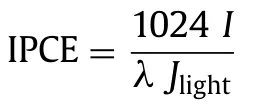
where the characterIstand for the photocurrent density,λis the wavelength of the incident light,andJlightrepresents the incident light power intensity.The IPCE data showed that the photo-active range of 1L MoS2/Cu2O NRAs vdWs heterostructure photocathode covers the full visible light range (350–700 nm) (Fig.5f).And the IPCEs of 1L MoS2/Cu2O NRAs photocathode were much higher than that of the Cu2O NRAs photocathodes in the range between 350 nm and 700 nm.The maximal IPCE value is up to 28% at 540 nm.These results all suggested that the strain tuned p-n heterostructure can effectively improve the PEC efficiency of photoelectrode,which can be attributed to the synergistic effect of band offset in the p-n heterointerface and strain gradient.
In summary,we have successfully prepared a 1L MoS2/Cu2O vdWs heterostructure photocathode material by nanoindentation technique.The effects of strain on promoting charge separation were verified by the enhanced performances in PEC hydrogen evolution reaction of vdWs heterostructure.The interfaces in the vdWs heterostructure were investigated by various characterization.Insituobservations further reveal that strain can be accurately applied in the vdWs heterostructure by controlling the height of the Cu2O NRAs.This work demonstrates the strain modulation is an effective method for regulating interface charge and promoting photoelectrochemical efficiency.Moreover,due to the large family of novel 2D materials and the compatibility of van der Waals heterostructures based on them,our results demonstrate a versatile method for the fabrication of effective PEC system and accurate understandings of the charge transfer processes in heterostructure.Furthermore,the strain engineer is introduced as a strategy of tunning the charge separation in mixed-dimensional vdWs heterostructures and is expected to be widely used in photoelectrochemistry,photo/electro-catalysis,photo-electronics,and so on.
Declaration of competing interest
The authors declare no competing interests.
Acknowledgments
The experimental work was supported by the National Key R&D Program of China (Nos.2018YFA0306900 and 2018YFA0209500),the National Natural Science Foundation of China (Nos.21872114,21972121 and 21908253),the Science and Technology Plan Project of Guangdong Province (No.2018A030310300),and the China Postdoctoral Science Foundation (No.2020M682616).Acknowledgment is made to the Donors of the American Chemical Society Petroleum Research Fund for partial support of this research (No.61155-DNI5).H.Ren and M.Li also thank the Defense Advanced Research Project Agency (DARPA) and the Army Research Office for the financial support (No.W911NF-20-1-0304).
Supplementary materials
Supplementary material associated with this article can be found,in the online version,at doi:10.1016/j.cclet.2021.08.062.
 Chinese Chemical Letters2022年3期
- Chinese Chemical Letters的其它文章
- Direct catalytic nitrogen oxide removal using thermal,electrical or solar energy
- Construction and applications of DNA-based nanomaterials in cancer therapy
- Recent research progress of bimetallic phosphides-based nanomaterials as cocatalyst for photocatalytic hydrogen evolution
- Nanostructured materials with localized surface plasmon resonance for photocatalysis
- Recent progress of Pd/zeolite as passive NOx adsorber: Adsorption chemistry,structure-performance relationships,challenges and prospects
- Microfluidic methods for cell separation and subsequent analysis