
H2S-assisted growth of 2D MS2 (M=Ti,Zr,Nb)
2022-06-18 10:53YiweiZhngPengZhngTengfeiXuXingguoWngHuningJingYongjiGong
Chinese Chemical Letters 2022年3期
Yiwei Zhng,Peng Zhng,∗,Tengfei Xu,Xingguo Wng,Huning Jing,Yongji Gong,∗
a School of Materials Science and Engineering,Beihang University,Beijing 100191,China
b State Key Laboratory of Infrared Physics,Shanghai Institute of Technical Physics,Chinese Academy of Sciences,Shanghai 200083,China
Keywords:Chemical vapor deposition Growth mechanism 2D transition-metal dichalcogenides Titanium disulfide FET properties
ABSTRACT 2D transition metal dichalcogenides (TMDCs) have drawn an enormous amount of attention due to their fascinating properties and application potential in next-generation information process and storage.However,the lack of proper synthesis approach limits their application.Here,we report a controllable synthesis method to grow ultrathin MS2 (M=Ti,Nb,Zr) nanosheets with H2S-assisted chemical vapor deposition (CVD).We found that the presence of H2S plays an important role to control the morphology of nanosheets including the lateral size and the nucleation density.With the assistance of H2S,the growth of MS2 shows much thinner thickness with largely decreased nucleation density,beneficial for the device application,which can be attributed to the kinetics dominated growth.Our method hence opens a new avenue for the CVD growth of 2D TMDCs and the corresponding heterojunction,and paves the way for exploring their intriguing properties and applications.
Two-dimensional (2D) transition metal dichalcogenides(TMDCs) are layered materials with fascinating properties,like the quantum spin Hall effect [1],valley polarization [2]as well as a wide range of potential applications [3],like field-effect transistors[4,5],photodetectors [6]and functional devices [7,8].Among them,the growth of semiconducting VIB group TMDCs such as MoS2and WSe2has been well realized and their applications in various fields have been systematically studied [9–13].In contrast,the growths of some metallic or narrow band-gap 2D materials with promising properties are still in their infancy.Titanium disulfide(TiS2) and niobium disulfide (NbS2),for example,have attracted increasing interests for their devisable electronic properties [14–18]and show application potentials as promising localized surface plasmon resonance materials [19]and superconductors.Another example,zirconium disulfide (ZrS2) with a smaller band gap than MoS2displays high carrier mobility and unusual electronic properties [20],which brings the potential applications in nanoelectronics [21]and photodetectors [22–24].However,many issues are remained to be tackled in the controllable synthesis of these ultrathin TMDCs nanosheets.
Several top-down methods,such as mechanical exfoliation [25],electrochemical lithium intercalation exfoliation and liquid sonication exfoliation [26,27],illustrate considerable handleability in the preparation of typical TMDs,black phosphorus (BP).However,it is usually difficult to control the shape,lateral size and thickness of the obtained nanosheets [28,29].Recently,bulk layered compounds[30]or large-size [31]TiS2flakes can be synthesized by chemical vapor transport (CVT) technique or a mixed-method of physical vapor deposition (PVD) and electron beam evaporation.Meanwhile,it is reported some substrates,such as h-BN and transferred graphene,are applied to synthesize ultrathin 2D nanocrystal by CVD [32,33].Nevertheless,the uniformity of the as-grown samples and the repeatability of these approaches are still not very satisfactory.
Herein,we report a highly reproducible synthesis of MS2(M=Ti,Nb,Zr) nanosheets using H2S-assisted CVD.By adjusting the growth parameters,like the growth temperature and the H2S flow rate,the size and thickness of the flakes can be well controlled.Various characterization techniques confirm the high quality of the as-synthesized MS2nanosheets and FET devices based on TiS2nanosheets show narrow band-gap semiconductor behavior and a thickness-dependent resistance.
The layers of MS2(M=Ti,Nb,Zr) are stackedviarelatively weak van der Waals interactions.In each layer,M (M=Ti,Nb,Zr) atoms are sandwiched by six sulfur atoms.Fig.1a shows the schematics of the growth of MS2(M=Ti,Nb,Zr) films on SiO2/Si substratesviaa CVD system together with the typical atomic structure of obtained MS2(M=Ti,Nb,Zr) from the side-view.More details about the growth process and experimental setup are provided in the Experimental Section and Fig.S1 (Supporting information).Briefly,sulfur powder and MOx/NaCl mixture were used as the reactants,where NaCl powder can help to decrease the energy barrier for the reaction and thus increase the growth rate[34].Ar is used as carrier gas and H2S is introduced only at the high temperature around 800 °C for about 3 min to get ultrathin nanosheets.The typical optical microscopy (OM) images of asgrown MS2(M=Ti,Nb,Zr) nanosheets with H2S-assistance are displayed in Figs.1b-d,where the as-synthesized samples display obvious contrast with the SiO2/Si substrates.The height profiles in Figs.1b-d show a smooth surface with the thickness of ∼2.4 nm for TiS2,∼1.3 nm for ZrS2and ∼1.8 nm for NbS2,respectively.And their corresponding AFM height images of the representative MS2(M=Ti,Nb,Zr) nanosheets are listed as Fig.S2 (Supporting information).Furthermore,the effect of H2S on the nucleation density and lateral size of these three kinds of samples are shown in Figs.1e-g.As shown,the presence of H2S can significantly reduce the nucleation density of TiS2,ZrS2and NbS2,thus,leading to much increased lateral size of the products.
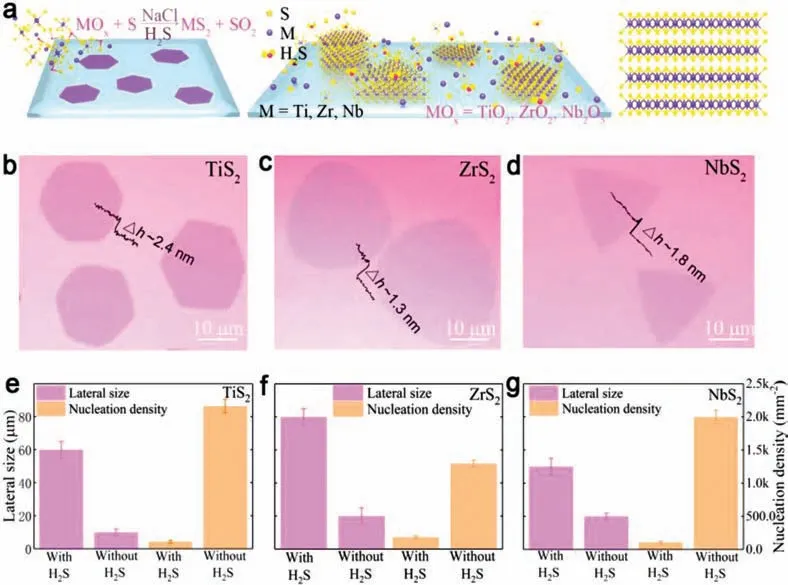
Fig 1.Synthesis of MS2 (M=Ti,Nb,Zr) nanosheets.(a) Schematic illustration of MS2 synthesis.(b-d) Typical OM images of MS2 nanosheets grown on SiO2/Si substrates with the corresponding height line profiles.(e-g) Sample statistical graphs of the lateral size and nucleation density of products grown with or without the assistance of H2S.
To find the optimal conditions for the growth of TiS2nanosheets,synthesis temperature and H2S flow are investigated in detail (Fig.2).Keeping the other growth parameters (growth time,carrier gas,precursor quantity,etc.) constant,H2S as auxiliary gas can obviously reduce the nucleation density and increase the lateral size of the samples compared to the growth without using H2S.Figs.2a-d show the typical OM images of TiS2grown from 750°C to 900°C without the help of H2S,where the thickness increases and the lateral size changes little with increased growth temperature.Figs.2e-h display the revolution of typical OM images of TiS2grown with 2 sccm H2S from 750°C to 900°C,in which the lateral size increases first and then the thickness becomes thicker.The corresponding statistical histogram of the number of layers increasing with temperature can be seen in Fig.S3 (Supporting information).The statistical histograms of the lateral size and nucleation density in Figs.2i and j show the effect of H2S clearly.The lateral size of TiS2nanosheets increases from ∼5 μm to ∼50 μm when introducing H2S while the nucleation density decreases from∼3k mm−2to ∼0.5k mm−2.In addition,the change of lateral size with different temperature is observed,which may be caused by the kinetic and thermodynamic process including the source sublimation rate,the nucleation rate,the growth rate and the stability of the products [35,36].At relatively low temperature,the growth process is largely kinetically controlled [37].With higher concentration of the reactants vapor at a little bit higher temperature,the product will prefer to deposit on the edge with high activity,which will lead to lateral growth.However,the growth is more thermodynamically controlled with further increased temperature,which will lead to thicker samples.Also,the supersaturated vapor source tends to increase the nucleation rate.As a result,the nanosheets tend to be thicker and smaller.However,the introduction of H2S could promote the growth of TiS2in the lateral dimension from both thermodynamics and kinetics,which will be discussed in detail in the following part.The above experimental results confirm that ideal ultrathin TiS2nanosheets could be gained at 800°C with the assistance of H2S.The same research methods are used to the synthesis of ZrS2and NbS2and the characterization of the asgrown nanosheets can be seen in Supporting information (Figs.S4 and S5),showing similar effects of H2S on the morphology control.
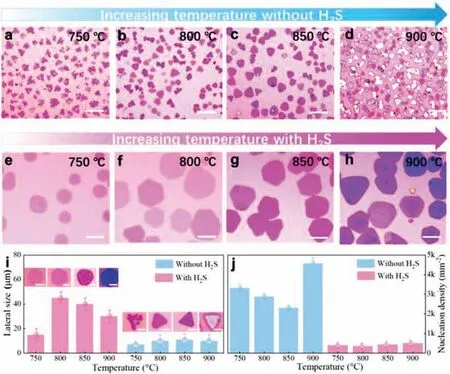
Fig 2.Typical OM images of TiS2 flakes grown under different conditions.OM images of TiS2 nanosheets grown without H2S at (a) 750°C,(b) 800°C,(c) 850°C,(d)900°C,respectively.OM images of TiS2 nanosheets grown with the assistance of H2S at (e) 750°C,(f) 800°C,(g) 850°C,(h) 900°C,respectively.(i) The lateral size as a function of the growth temperature with the corresponding OM images.(j) Nucleation density of TiS2 flakes as a function of the growth temperature.Scale bars in (a-i): 10 μm.
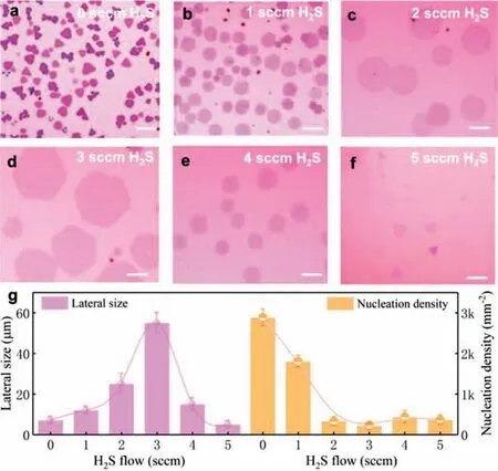
Fig 3.The effect of the flow rate of H2S on growing TiS2 nanosheets at 800 °C.(a-f) OM images of TiS2 nanosheets grown with H2S flow range from 0 to 5 sccm.All scale bars are 10 μm.(g) TiS2 lateral size and nucleation density as a function of the H2S flow rate.
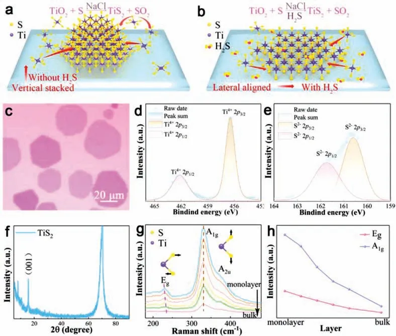
Fig 4.Phase characterizations of the as-grown TiS2.(a,b) Possible growth models of TiS2 nanosheets on SiO2/Si substrates.(c) Typical OM image of TiS2 films grown with 3 sccm H2S.(d,e) XPS characterization of Ti 2p and S 2p peaks of the as-grown TiS2 sample.(f) The XRD pattern of the TiS2 films flakes on SiO2/Si from a thick sample.(g)Raman spectrum of TiS2 nanosheets with different layers using a 532 nm excitation laser (including a representation of A1g and Eg vibrational modes).The dashed line in Eg highlights a minor change of the peak position.(h) Peak intensity change of the A1g and Eg vibrational mode as a function of layer numbers.

Fig 5.TEM characterization of the as-grown TiS2.(a) Low-magnification TEM image of TiS2 nanosheets.(b) The high-resolution TEM image.(c) The corresponding fast Fourier transform (FFT) image.(d) Representative EDS spectrum for the as-grown TiS2 and the corresponding elemental mapping images of Ti (e) and S (f) elements.
To deeply understand the mechanism of how H2S critically affects the synthesis of TiS2nanosheets,the effect of H2S flow rate on the reaction is studied in detail.Figs.3a-f illustrate the OM images of TiS2grown at 800°C with different H2S/Ar flow rate.Obviously,the nucleation density and domain size are very sensitive to H2S flow rate.With the increase of H2S flow,the lateral size firstly increases and then decreases while its nucleation density firstly decreases and then keeps constant.Thus,3 sccm H2S flow rate is the best condition that can get the maximum size of TiS2nanosheets (about 60 μm).The experimental phenomenon shows that a small H2S flow can significantly decrease the nucleation density (Fig.3g),which is beneficial for achieving a large domain size at the proper growth time and growth temperature.A simple growth mechanism model and typical OM images of TiS2nanosheets are speculated in Figs.4a-c.Firstly,compared to S,H2S could help to produce more active Ti intermediate products with higher Gibbs free energy,which could further lower theΔGof the reaction.This will further minimize the thermodynamic stability difference of the lateral growth product and vertical growth product.In this case,the dynamics will play a more dominant role and the source atoms will quickly add to the edge sites to realize the lateral growth [37].Secondly,the high activity of H2S can react with the TiO2/NaCl powder before its evaporation,this could decrease the vapor pressure of Ti species to obtain a low nucleation density.Thus,further increasing the flow rate of H2S will inhibit the growth of TiS2on the substrate.
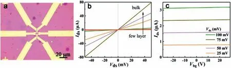
Fig 6.Electrical measurement of the TiS2 nanosheets.(a) The OM image of a fabricated device based on TiS2 grown on SiO2/Si substrate.(b) Ids-Vds curve of the TiS2 device collected at room temperature.(c) The transfer characteristic curves of the devices.
X-ray photoelectron spectroscopy (XPS) was further conducted to study the chemical states and elemental composition of the asgrown samples.As Figs.4d and e shown,the chemical states of Ti4+2p3/2and 2p1/2can be identified from the peaks at ∼456 and 462 eV (Fig.4d) and the peaks at ∼160 and ∼162 eV (Fig.4e) correspond to the 2p3/2and 2p1/2states of S,respectively.The elemental composition of Ti:S perfectly matches the stoichiometric ratio of 1:2.
X-ray diffraction (XRD) characterization was performed on a thick sample to further identify the crystal structure of the asgrown samples.As shown in Fig.4f,the peak at 2θ=15.56° of the CVD-grown sample matches well with the (001) crystal planes of TiS2reported in the literature [29,38].The peak at 2θ=69° can be indexed to the Si substrates.Raman characterization with 532 nm laser is further applied to characterize the grown samples,as shown in Fig.4g.It shows a peak at ∼230 cm−1ascribed to the inplaneEg,a peak at ∼330 cm−1corresponding to out-of-planeA1gmodes,and a shoulder mode at about 375 cm−1assigned toA2u,which is consistent with reported literature of TiS2[29].When the thickness increases,theEgpeak exhibits a blueshift from 228 cm−1(monolayer) to 236 cm−1(bulk) while theA1gpeak at ∼330 cm−1shows a negligible shift.Fig.4h further summarizes the evolution of Raman intensities with thickness,showing decreased intensity of bothEgandA1gpeaks with increased thickness.
Further,transmission electron microscope (TEM) was performed on the transferred samples to investigate the detailed atomic structures of TiS2samples.The low-magnification TEM image (Fig.5a)shows a typical TiS2flake on the lacey carbon films supported by Cu grids.Fig.5b shows a high-resolution TEM (HRTEM) image of the sample,displaying a good atomic arrangement.The lattice spacing of ∼1.70 and ∼2.93 ˚A matches the predicted spacing for the (110) and (100) planes of 1T-TiS2.The corresponding fast Fourier transformation (FFT) image (Fig.5c) presents only one set of hexagonal diffraction spots,which confirms the single-crystal nature and high crystal quality.Energy dispersive spectroscopy(EDS) employed along with TEM on the transferred samples identifies the chemical composition of ∼1:2 for Ti:S in Fig.5d.The EDS maps (Figs.5e and f) clearly exhibit the spatial distribution of Ti and S atoms and their uniform color distribution demonstrates the compositional uniformity of the synthesized TiS2nanosheet.Together,these TEM results confirm that the H2S-assisted CVD method can obtain ultrathin single-crystal TiS2nanosheets with high quality.
In addition,electrical measurements were performed on a series of FETs based on the as-grown TiS2samples with different thickness.Fig.6a exhibits the OM image of a typical fabricated device with a channel width (W) of 8 μm and channel length (L) of 7 μm.The Ti/Au electrodes were made directly on the samples using photolithography and e-beam metal deposition (more details are provided in the Experimental Section in Supporting information).Fig.6b shows the thickness-dependent resistance of TiS2devices,exhibiting that the resistance decreases with the increase of thickness.The corresponding linear current-voltage (Ids-Vds) curve collected at room temperature also demonstrates an Ohmic contact at the interface.The transfer characteristic curves of the devices under differentVdsin Fig.6c demonstrate the narrow bandgap semiconductor behavior of the TiS2channel [39,40].
In summary,we have introduced H2S to assist the synthesis of several 2D transition-metal dichalcogenide materials,such as TiS2,NbS2and ZrS2,in an ambient pressure CVD system.Further XRD,TEM and Raman characterizations reveal that the nanosheets are single crystals and possess high crystallinity.We take TiS2as an example to study the role of the H2S in the growth,where H2S can effectively inhibit the growth in the vertical direction and reduce the nucleation density due to its high reactivity.The method provides direct access to highly crystalline TiS2,ZrS2and NbS2nanosheets,with superior controllability over the growth morphologies,such as the domain size and thickness.Our study hence suggests a promising CVD paradigm to synthesize high quality various 2D atomic crystals.It also provides a possible inspiration for the preparation of other 2D TMDCs and opens up opportunities for exploring a variety of intriguing physics,corresponding properties and applications of 2D TMDCs.
Declaration of competing interest
The authors declare that they have no known competing financial interests or personal relationships that could have appeared to influence the work reported in this paper.
Acknowledgments
This work was supported by the National Key R&D Program of China (No.2018YFA0306900) and the National Natural Science Foundation of China (No.51872012).
Supplementary materials
Supplementary material associated with this article can be found,in the online version,at doi:10.1016/j.cclet.2021.07.036.
 Chinese Chemical Letters2022年3期
- Chinese Chemical Letters的其它文章
- Direct catalytic nitrogen oxide removal using thermal,electrical or solar energy
- Construction and applications of DNA-based nanomaterials in cancer therapy
- Recent research progress of bimetallic phosphides-based nanomaterials as cocatalyst for photocatalytic hydrogen evolution
- Nanostructured materials with localized surface plasmon resonance for photocatalysis
- Recent progress of Pd/zeolite as passive NOx adsorber: Adsorption chemistry,structure-performance relationships,challenges and prospects
- Microfluidic methods for cell separation and subsequent analysis