General Galois Processor for Transmitters in 5G/6G Base Stations
Qingbo Zhai,Yong Bai,Dake Liu
State Key Laboratory of Marine Resource Utilization in South China Sea,College of Information and Communication Engineering,Hainan University,Haikou 570228,Hainan Province,China
Abstract:This paper proposes a flexible eight-mode high parallel Galois SIMD ASIP(Application Specific Instruction Set Processor).It supports parallel executions of Gold,Scrambling,CRC,CC,Turbo,RM,PSS,SSS encoding LFSR(linear feedback shift registers)algorithms with high performance and flexibility.It can perform also general bit processing and m-sequence.Our design is based on proposed table conversion and a datapath for unified eight-mode encoding.Based on 28 nm digital CMOS technology,the total area is 0.177mm2 and the clock frequency can be up to 1 GHz.The throughputs of Gold,Scrambling,CRC32,CRC24,CRC16,CRC8,CC,Turbo are 64Gb/s,64Gb/s,128Gb/s,168Gb/s,256Gb/s,512Gb/s,3×80Gb/s,and 72Gb /s,respectively.
Keywords:multi-mode parallel encoding;ASIP;SIMD;URLLC;5G base station
I.INTRODUCTION
The communication encoding algorithms involve bitlevel operations and they cannot be directly executed in parallel since such algorithms are iterative.The flexibility of classical circuit solution is not enough to meet the base station requirements.The performance and process delay of classical software solutions are not acceptable.Industries need a solution to offer both flexibility(adapt changing of algorithms and standards)and efficiency(with high parallel degree and low process latency).
Parallelization for not-parallel-able algorithms is one of the well-known hard problems and it brings a challenge for short-delay broadband communication baseband encoding.According to the 3GPP standard[1—4],Gold,Scrambling,CRC,CC,Turbo,PSS(5G)and SSS are implemented using LFSR,an iterative algorithm using feedback data.It can only process 1bit data in one machine cycle and seemingly cannot be parallelized.Nowadays,the demand for high-speed data transmission is increasing so that the TTI(Transmission Time Interval)of URLLC(Ultra Reliable Low Latency Communication)is required to be reduced to sub-milliseconds.As the basic technology of the physical layer,channel coding must be executed with low latency.Therefore,the parallelization of LFSR is essential for 5G/6G.Luckily it can be resolved by SIMD architecture running Galois Field arithmetic[5].Furthermore,a unified design framework can be feasible because these LFSR algorithms can all be implemented in parallel by state parallel space conversion matrix(state-space conversion matrix[6])using parallel LUT(look-up table)method.The use of the SIMD architecture and bit-slicing[7]enables Galois ASIP to achieve high parallelism and low computing latency at a low silicon cost.
Aforementioned parallel method can be implemented by ASIC,FPGA,and general processors.However,ASIC as a fixed circuit is not enough flexible,the price of FPGA is too high,and the performance of general processor is low.The rest of the paper will demonstrate that our Galois ASIP is so far the best solution within bit manipulation domain thanks to its dedicated instruction set architecture offering the high performance and flexibility,as well low cost by the same solution.
We built a processor supporting eight-mode LFSRrelated parallel encoding algorithms.To our best knowledge on available references,no previous work can achieve the goal.There were many single-mode circuits with parallel implementations[8—10]or dualmode parallel schemes[11,12].Reference[8]realized Gold coding with a maximum parallelism of 6;[9]realized convolutional coding with a parallelism of 8;[10]realized turbo parallel coding with a throughput of 9.595Mbpc;[11]introduced an EDA tool that can generate circuits for parallel CRC and parallel Scrambling,the maximum parallelism of CRC and Scrambling is 64 and 32.Some of these schemes cannot be massively parallelized and some cannot be adapt to multi-mode.In[12],a multi-standard and high-parallel CRC encoding and RS decoding is realized,which showed the potential of the look-up table method in high parallelism and fusion.
The rest of the paper is arranged as follows:Section II introduces the eight encodings we have involved and contributions of our work;Section III highlights the mapping from algorithm to architecture and eight-mode unified data path;Section IV introduces the hardware design of Galois ASIP.Section V exposes simulation verification of our design and the comparison to references.Section VI concludes this paper.
II.EIGHT ENCODINGS OF GALOIS ASIP
In 5G/6G mobile communication systems,Gold coding has good cross-correlation characteristics;Scrambler processes bit-level randomization before transmission,effectively improves the accuracy and reliability of data detection;CRC(Cyclic Redundancy Check)is for error detection with low detection cost;Convolutional coding offers strong error correction capabilities,and is suitable for low latency serial transmission;The error correction capabilities of Turbo coding close to Shannon’s limit.RM(Reed-Muller)code offers multi-bit error detection and correction.PSS(Primary Synchronization Signal)and SSS(Secondary Synchronization Signal)are for UE synchronization with base station and also for passing physical cell identification PCI or NCellID.The configurations of these coding algorithms keep varying and are complicated.It is thus excellent to implement a parallel programmable coding processor offering high performance and flexibility the same time.
We thus offer our contributions as follows:
1:We propose an innovative multi-mode architecture,we are the first one merged 8 modes into a unified architecture;
2:We pre-calculate all step results and store them in LUT,and then use parallel input data as the LUT address,instead of using hardware circuits with no flexibility;
3:We define and realize flex ASIP instructions and LUT as well the unified architecture,it offers strong flexibility to allow algorithm and standard changes;
4:We provide enough throughput for transmitters in 5G/6G base stations;
5:The silicon implementation proves high quality of our design;
In summary,our research results significantly reduced TTI for URLLC in 5G and 6G base stations.
III.ALGORITHMS
3.1 Mapping From Algorithm to Architecture
[6,13,14]provide mathematical method converting LFSR to its equivalent state-space form.Combining[8]and[15],we can summarize the following table:
Here ‘T’ stands for transpose.X(t+1)and Y(t+1)are vectors representing the parallel input and parallel output at the t+1 cycle,respectively.D(t+1)is a vector representing the value of the shift register after t+1 cycle.The feedback data is obtained in the current cycle and will be used in the next cycle.G is the state-space transition matrix[6,8,15]representing the input and output relation of the corresponding LFSR.
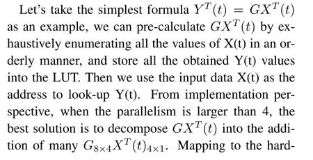
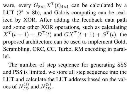

Table 1.Summary of parallel implementation formula.
3.2 Eight-mode Unified Data Path
We designed unified datapath as a core part for Galois ASIP.The core part consists of four steps:Prepare input data(input data permutation),Get pre-processed input data(Look-up table);Logic computing(XOR);and Result Selection and iteration(write permutation).All parallel calculations can be realized through this core part.As shown in Figure 1,the four modules of this core part are at the pipeline of execution stage as the longest critical path with delay of 0.78ns.All mentioned above are mapped into a SIMD architecture which implemented by two steps:bit-slicing technology and multipath parallel look-up table.
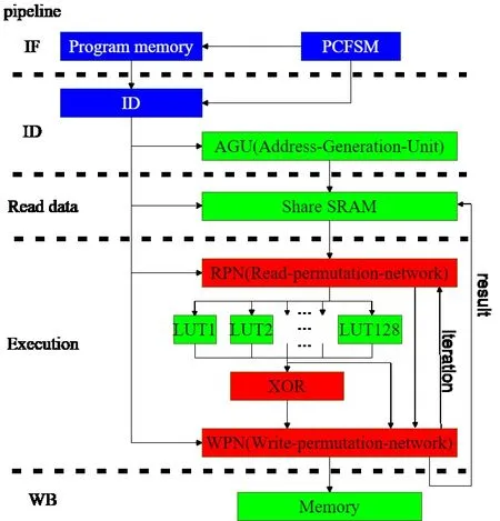
Figure 1.Top-level architecture.
To meet different communication standards,extra pre-processing and postprocessing circuits are required to adapt the differences.Our Galois ASIP realize all eight algorithms by adding pre-processing(adapt data to the parallel architecture by fill in zeros)before the core and post-processing(remove added zeros)after the core following[16].
IV.GALOIS ASIP HARDWARE DESIGN
4.1 Top-level Architecture
As shown in Figure 1,the top-level architecture consists of three parts:control logic(blue),storage subsystems(green)and data paths(red).Control logic calculates the PC to read an instruction from the program memory to instruction decoder in every clock;The share SRAM gives the coding input bits addressed by AGU(Address-Generation-Unit).RPN(Read-Permutation-Network)selects data for the core datapath from initial value,input,and iterative feedback.RPN also outputs 512=128×4-bit data to the LUT composed of 128 SRAM blocks(the size of each block is 16×8b).The LUT data is the step result of a target algorithm.In each clock,LUT provides a total of 128 bytes of data to XOR for Galois computing.XOR module outputs data to the WPN(Write-Permutation-Network).The WPN selects data from XOR module and RPN for reorder output or,sometimes,iteratively,for further Galois computing according to the algorithm in execution.The WPN also offers feedbacks for iteration.
4.2 FSM(Finite State Machine)and Instruction
The PC State Machine has four states:PC=0,PC=PC,PC=PC+1,PC=X.They are used to initialize PC value,single instruction loop,and normal execution,respectively.Galois ASIP has two states,normal and single instruction loop[17].The control path consists of a PC FSM with 5 pipelines.The simple ASIP has only 13 instructions.One instruction is used to load the pre-stored table and 12 instructions are used for Gold,Scrambling,CRC32,CRC24,CRC16,CRC8,CC,Turbo,RM,PSS,SSS5G,SSS4G encoding,where the command CRC32 is also used for general bit processing.We execute an algorithm using one instruction.In addition,RM,PSS,SSS encoding can be completed respectively in one machine cycle.
V.SIMULATION,VERIFICATION AND ANALYSIS
Our proposed design is synthesized using System Verilog implementation and Synopsys DC and IC Compiler with SMIC 28nm digital CMOS technology.We use 128×16×8b= 16384-bit registers instead of SRAM.The total cell area is 0.177mm2and the synthesized total peak power consumption is 117 mW(including the power consumed by back annotated capacitances).The power consumption is measured on 0.9V supply voltage at the clock frequency of 1GHz.Figure 2 describes the layout result where the die size without pin is 0.446mm×0.446mm.

Figure 2.Layout result.
Our Galois ASIP takes over the Turbo and CC encoding excepting for the Turbo and CC interpolation which are executed by another ASIP in our project.
Reference[8]realized a Gold encoding scheme with throughput of 6bpc,throughput of our Galois ASIP is 10.7 times of[8];[10]realized a turbo encoding scheme with throughput of 9.595bpc.The throughput of our Galois ASIP is 7.5 times of[10].There are[18]and[19]with 32bpc and 16bpc respectively for scrambling in 802.11.Our Galois ASIP can also achieve the same scrambling with a throughput of 512bpc by changing the configuration,which is 16 times of[18]and 32 times of[19].
The comparing result shows the superior performance of our Galois ASIP.Our Galois ASIP has high throughput by applying SIMD architecture running at high clock frequency(1GHz).It ensures high computing performance and low computing latency by specially accelerated instructions and meets the 5G standard requirements especially for URLLC.
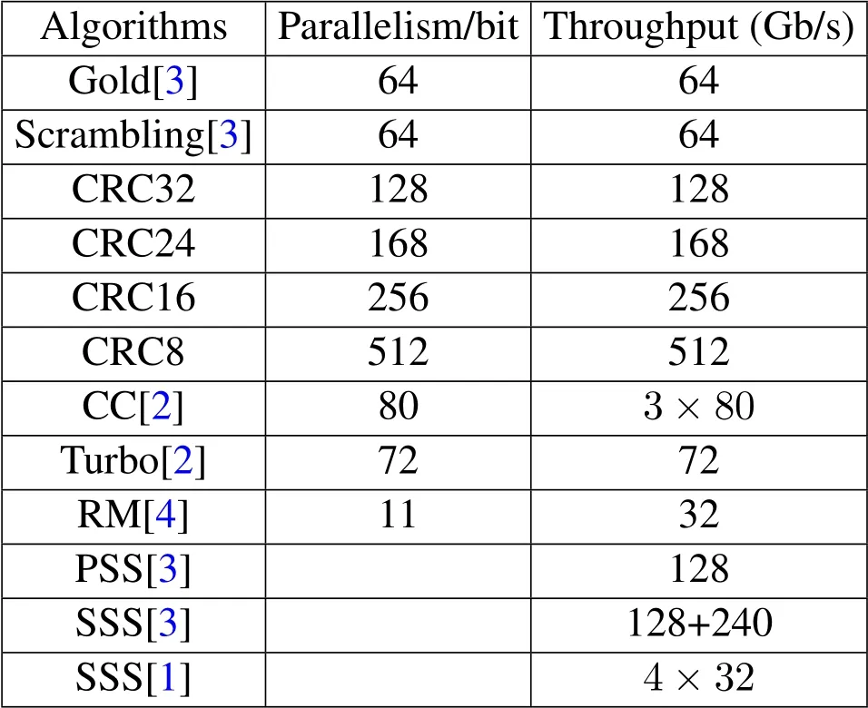
Table 2.Performance of our Galois ASIP.
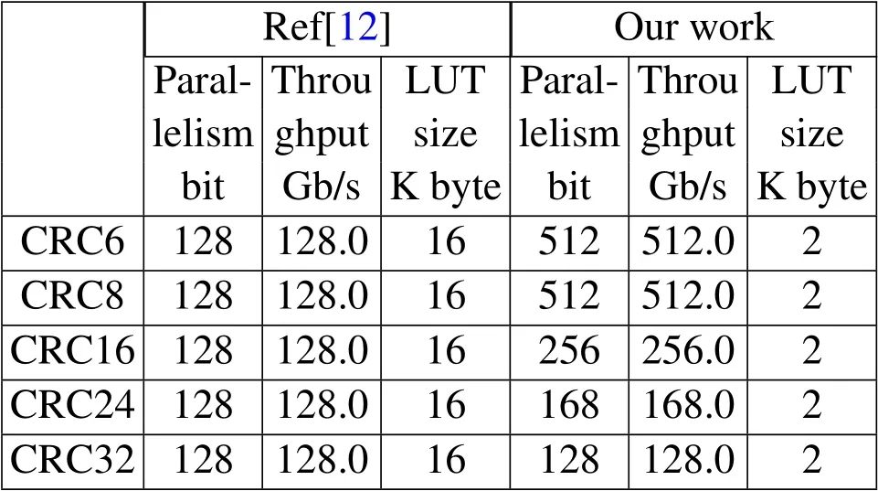
Table 3.Comparison between proposed processor and ref[12].
VI.CONCLUSION
This paper proposes a Galois ASIP as a flexible eightmode high-parallel ASIP for most encoding running in parallel in base station and terminals(except for Polar and LDPC encoding).It can be used as a general-purpose encoding processor.The Galois ASIP uses programmable hardware to support flexibility.It thus extend product life while keeping silicon costs at a reasonable level.It can highly accelerate general encoding algorithms,perform general bit processing and general encoding algorithms of eight algorithms.Our Galois ASIP can further support URLLC with ultra-low TTI[20],and can be a candidate technology for addressing the high-rate challenges of 6G in the future[21—24].According to reachable references,our Galois ASIP is the first solution implemented most encoding algorithms for sub-6G and millimeter-wave 5G and compatible 4G.We offered an encoding processor for base stations with an innovative implementation method.
ACKNOWLEDGEMENT
This work was supported in part by the Project of the National Natural Science Foundation of China(Grant No.61961014),and this work was also supported by the Hainan University project funding KYQD(ZR)1974.
- China Communications的其它文章
- Wireless Network Requirements and Solutions for the Future Circular Collider:A Hostile Indoor Environment
- On the Performance of Active Analog Self-Interference Cancellation Techniques for Beyond 5G Systems
- Multi Object Tracking Using Gradient-Based Learning Model in Video-Surveillance
- Catalyzing Random Access at Physical Layer for Internet of Things:An Intelligence Enabled User Signature Code Acquisition Approach
- A Task-Resource Joint Management Model with Intelligent Control for Mission-Aware Dispersed Computing
- Research on Online Education Consumer Choice Behavior Path Based on Informatization

