
Surface plasmon resonance characteristics of a graphene nano-disk based on three-dimensional boundary element method
2021-10-10 09:46WANGShuoHUBinLIUJuan
中国光学 2021年5期
WANG Shuo,HU Bin,LIU Juan
(School of Optics and Photonics, Beijing Institute of Technology, Beijing 100081, China)
* Corresponding author,E-mail: hubin@bit.edu.cn
Abstract: Compared with the commonly used simulation algorithms such as Finite Element Method (FEM)and Finite-Difference Time-Domain (FDTD) method, the Boundary Element Method (BEM) has the advantages of high accuracy, small memory consumption, and ability to deal with complex structures. In this paper,the basic principle of three-dimensional BEM is given, the corresponding program based on C++ language is written, and the Surface Plasmon Resonance (SPR) characteristics of a graphene nano-disk structure are studied. The Scattering Cross-Section (SCS) spectral lines of a graphene nano-disk under different chemical potentials, as well as the distributions of electromagnetic fields at the resonance wavelengths are calculated. The electromagnetic response of the graphene nano-disk in the infrared band is analyzed. In addition, considering the common corrugations of graphene materials caused by defects during processing, we study the influence of the geometric parameters of a convex structure in the center of the graphene nano-disk on the resonance intensity, wavelength and field distributions. A spring oscillator model of charge movement is used to explain the simulation results.
Key words: three-dimensional boundary element method; graphene; surface plasmon resonance; scattering characteristics
1 Introduction
When light is incident on the metal surface, the free charges in the metal will be driven by the incident light field to form collective oscillations with strong scattering, absorption or coupling. This characteristic is called Surface Plasmon Polaritons(SPPs) resonance. The SPPs have a strong local field enhancement effect. Because their transmission wavelength is smaller than that of incident light, they can be used in optical waveguide[1], lithography[2]and other fields. When the metal size is reduced to tens or hundreds of nanometers, the electromagnetic wave transmitted along the surface will be confined on the surface, generating Localized Surface Plasmonic Resonance (LSPR). Since the resonance wavelength, resonance intensity and scattering spectrum of LSPR can be modulated by the material, shape and other factors of nanostructures,LSPR has been widely studied and applied in the fields such as biosensing[3], energy[4]and information[5].
Graphene is a two-dimensional crystal made of a single layer of carbon atoms linked into honeycomb lattices[6], and is a good LSPR material with strong local field enhancement effect and low loss.In addition, the properties of graphene can be adjusted by the methods such as chemical doping and applied electric field, so graphene can be made into a new type of LSPR optical device with external modulation[6]. Graphene has a broad application prospect in optical waveguides[7-9], biosensors[10], metasurfaces[11], metamaterials[12,13], photoelectric devices[14]and other optical fields. Graphene nanodisk is a commonly used graphene structure. C.X.Cong et al.successfully prepared an ordered graphene nanodisk array by combining nanospheric lithography with reactive ion etching[15]. Sukosin Thongrattanasiri et al. investigated the application of graphene nanodisks in optical absorption and demonstrated a periodic graphene nanodisk array capable of achieving 100% optical absorption[16]. Zheyu Fang et al.proposed a tunable optical absorber based on graphene nanodisks and investigated the relationship between its absorption characteristics and the size, spacing and chemical potential of the nanodisks[17]. Hugen Yan et al. studied the coupling effect of graphene nanodisks and proved that different coupling modes would lead to different electromagnetic responses[18]. Jialong Peng et al. reported the study of a tunable terahertz half-wave plate based on coupled graphene nanodisks, using a reflective structure to achieve the function of half-wave plate[11]. Lauren Zundel et al. achieved infrared molecular sensing with subwavelength-level spatial resolution by utilizing the electrical tuning properties of the plasmon polaritons of graphene nanodisk arrays[19]. Vasilios D. Karanikolas et al. studied the role of graphene nanodisks between quantum emitters and demonstrated that the strong resonance of graphene nanodisks could increase the interaction distance between quantum emitters by an order of magnitude[20].
However, all of these studies focused on the ideal planar graphene. As a kind of flexible material,graphene can produce convex/concave structures,corrugations and other non-planar defects in the machining process.
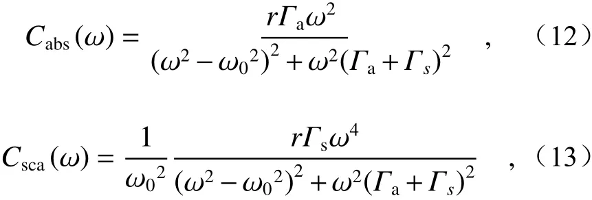
Meanwhile, with the progress of modern micro-nano machining technique, the three-dimensional structures with surface corrugations can also be fabricated by artificial stretching, squeezing, mechanical vibration and other methods, and their dimensional parameters can be controlled[21-23]. These three-dimensional structures can also modulate the SPP resonance of graphene. Penghong Liu et al.studied the SPP resonance mode of wedge-shaped graphene waveguides and obtained the SPP propagation constants and local field distributions in different modes[8]. Slipchenko et al. studied the SPP reflection properties of corrugated graphene layers and quantitatively described the effect of corrugations on the reflection intensity[24]. Shengxuan Xia et al. demonstrated the tunable electromagnetically-induced transparency of sinusoidal graphene layers[25].Li Wang et al. investigated the LSPR properties of bent graphene nanoribbon arrays molded on soft substrates and discovered a new decoupling mechanism[26]. However, the above studies were all based on two-dimensional structures. There are few reports on the non-planar graphene with a three-dimensional defect structure.
In this paper, the three-dimensional boundary element method (3D-BEM or BEM) was used to study the SPR properties of flat and convex graphene nanodisks. Compared with other simulation algorithms in common use, the 3D-BEM can simplify the calculation of three-dimensional objects into the solution of the surface field of objects,that is, it can reduce the three-dimensional calculation to two-dimensional calculation. Therefore, this method can reduce the occupation of computer resources, and improve the calculation speed. We have written a 3D-BEM numerical calculation program based on C++ language. From the calculation results, it can be seen that the incident light in the mid-infrared band can stimulate the SPR phenomenon of graphene structure. By adjusting the electrochemical potential of graphene, we found that the resonance wavelength, the scattering intensity, and the FWHM (Full Width at Half Maximum) of the spectral lines all changed regularly. By adding a convex structure to the graphene structure, the scattering spectrum can also be shifted. We have made necessary explanation of the change law given in this paper by using the law of charge motion and the spring oscillator model. Our research will help understand the LSPR properties of graphene, and also expand the application of BEM algorithm.
2 3D-BEM theory
The schematic of scattering in three-dimensional space is shown in Fig. 1. In an isotropic free space, there is a three-dimensional scatterer, which is hit by infinite incident light. The scatterer surfaceSdivides the scatterer space into two parts, namely the outer regionV2and the inner regionV1. The outer normal vector of the scatterer is →n. The refractive index, relative dielectric constant and permeability of the regionV1aren1,ε1andμ1, respectively. The refractive index, relative dielectric constant and permeability of the regionV2aren2,ε2andμ2, respectively.
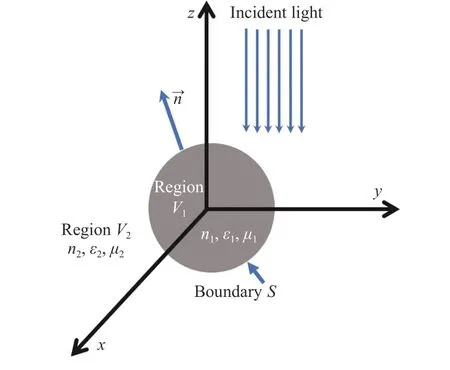
Fig. 1 Schematic of three dimensional scattering图 1 三维空间散射示意图
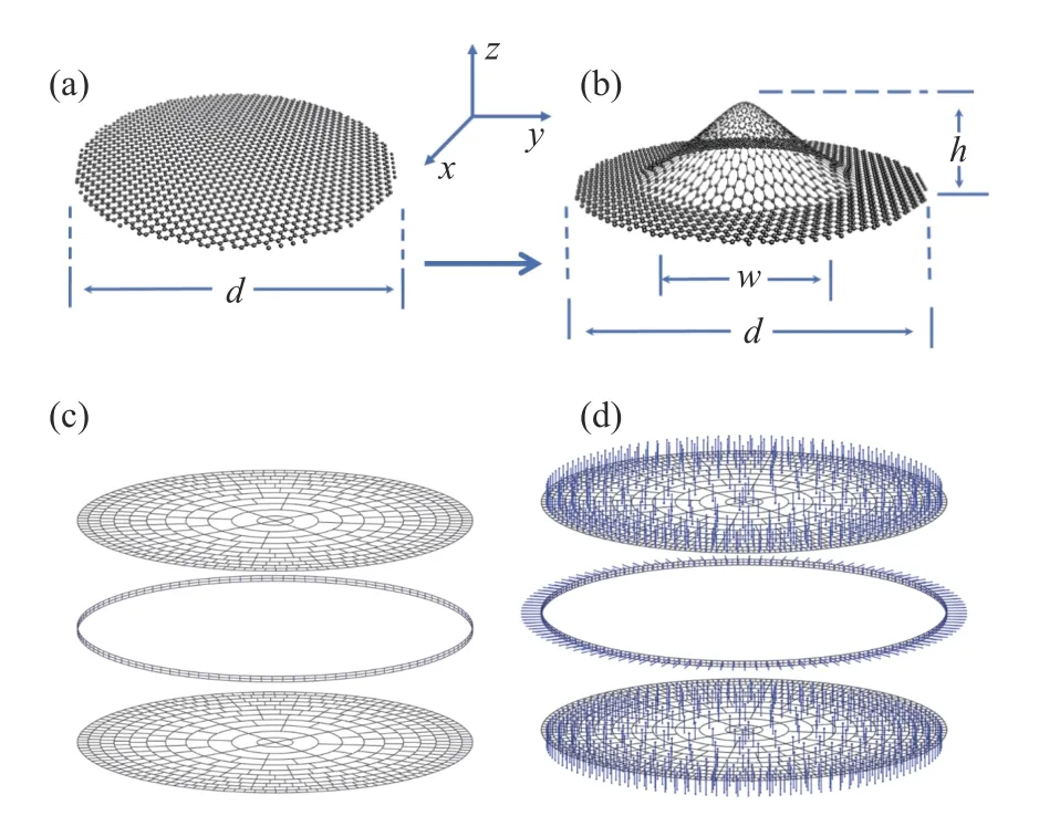
Fig. 2 Graphene model and surface-element division method (a) Graphene nanodisk model; (b) convex graphene nanodisk model; (c) mesh generation of graphene nanodisk model; (d) outer normal vectors of the meshes generated in graphene nanodisk(shown by blue arrows)图 2 石墨烯模型以及面元划分方法(a)石墨烯圆盘模型;(b)凸起石墨烯圆盘模型;(c)石墨烯圆盘建模的网格划分;(d)石墨烯圆盘所建网格的外法向矢量(蓝色箭头所示,见网络彩图)
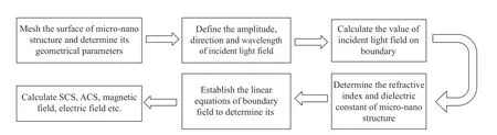
Fig. 3 Flow chart of boundary element method图 3 边界元算法流程图
By combining the classical Maxwell's equations with Green's function of vector potential, the following equations can be derived to show the distribution of electric and magnetic fields in the whole space[27]:


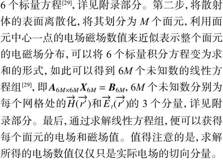
Next, we present the numerical method ofFirstly, the vector equations (3)and (4) are decomposed inx,yandzdirections to obtain 6 scalar equations[29], as shown in the appendix. Secondly, the surface of the scatterer is discretized and then divided intoMsurface elements.By using the values of electric and magnetic fields at the center of a surface element to approximate the electric and magnetic field distributions of the whole surface element, we can express the 6 scalar integral equations in the form of summation. Thus we can obtain the linear equation set of 6Munknowns[29], namely A6M×6MX6M=B6M. The 6Munknowns are the three components ofandin every surface elements, respectively, as shown in the appendix. Finally, by solving the linear equations, we can obtain the electric and magnetic field values of each surface element. It is worth noting that the calculated electric field value is only the tangential component of the actual electric field.
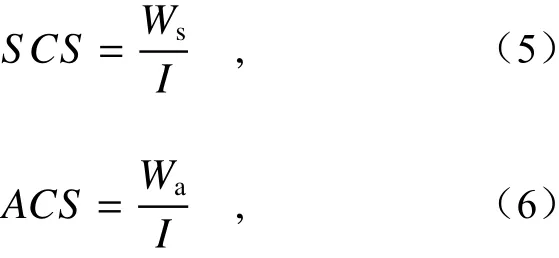
After the distributions of electric and magnetic fields on the surface of the scatterer are obtained,the magnetic field at any point in space can be obtained by further discretizing the equation (1) and equation (2). Then, by using Maxwell's equationthe electric field at this point can be calculated, and the distributions of electric and magnetic fields in the whole space can be obtained.After that, we can calculate other physical quantities, such as Scattering Cross Section (SCS), Absorption Cross Section (ACS), etc.
The SCS and ACS can be calculated by using the equations (5) and (6)[30]:

whereWsandWaare the scattering power and the absorption power. They can be calculated by using a closed surfaceГsurrounding the scatterer and the energy flux density (Poynting vector):


3 Modeling of the graphene nonadisk
We first consider the graphene nanodisk structure, with a diameter ofd=60 nm, located in thex-yplane, as shown in Figure 2(a). To study the graphene structure with a defect, we assume that there is a bulge at the center of the graphene nanodisk. This convex structure can be obtained by the mechanical vibration of a resonator[23]. The height of the bulge ish, as shown in Figure 2(b). The width of the bulge, marked as “w”, is defined as the length when the height is changed intoh/exp(1). Then the coordinates of the wrinkled nanodisk in thezdirection can be described as:
Next, we need to divide the surface elements of the graphene nonodisk structure through mesh generation. In the modeling process, the graphene thickness is set as 1 nm[32]. We consider the graphene nanodisk as a cylindrical model with very small height. Since the thickness of two-dimensional graphene material is very small relative to the size of the whole structure, the calculation instability can be caused easily. Therefore, an appropriate mesh generation method should be selected. The mesh generation here mainly follows the following two principles. Firstly, the aspect ratio of each mesh must not be too large. The maximum aspect ratio in this paper is 1.5:1. The structural change in the edge area is more complex than that in the central area, so the edge meshes should be denser. According to these two principles, meshes are generated in the disk, as shown in Figure 2(c). The upper and lower surfaces are divided into 11 rings. The width of each ring and the number of surface elements are shown in Table 1.
The flank is divided into two layers, each of which has 116 surface elements. Therefore, there are 1224 surface elements in total. The position of the center point of each face element and its outer normal vector are shown in Figure 2(d) (Color online). The mesh generation in a convex structure is realized by projecting the meshes of flat disk structure onto the convex structure along thezaxis.

Tab. 1 Parameters of mesh generation on the upper and lower surfaces of graphene nanodisk表 1 石墨烯纳米圆盘上下表面网格划分参数
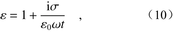
The optical parameters of graphene are calculated using the method in the reference [32]. Its dielectric constant can be calculated by the following equation:
whereε0is the vacuum dielectric constant,ωis the angular frequency of the incident light,σis the conductivity of graphene, i is the imaginary unit, andtis the thickness of graphene. The conductivity of graphene in the far-infrared and terahertz bands can be expressed as[7,33]:
whereeis the charge per unit,EFis the chemical potential of graphene, andτis the carrier relaxation time.
Our numerical calculation program is written in C++ language. Under the sub-surface element condition mentioned above, the program occupies about 1.6 G of memory. It takes about 5 minutes for an ordinary personal computer (configuration: i7-8550U,4.0 GHz, 8G RAM) to calculate a wavelength point.The calculation process of the whole algorithm is shown in Figure 3.
4 Simulation results and analysis
4.1 Comparison of the results from BEM and FDTD
In order to verify the correctness of the threedimensional boundary element program written, we first calculated the SCS spectrum of graphene nanodisk in the wavelength range of 5~11 μm and the electric and magnetic field distributions at the resonant position, and then compared the results obtained by BEM with those obtained by the commercial software Lumerical FDTD Solutions based on Finite-Difference Time Domain (FDTD) method. The graphene disk under calculation has a diameter ofd=60 nm and a chemical potential ofEF=0.25 eV.The incident light perpendicular to the disk and incident along the −zaxis is linearly polarized light,and the polarization direction of electric field is along theyaxis. The normalized SCS spectra of the two algorithms are shown in Figure 4(a) and Figure 4(d) respectively. It can be seen that, in the calculated band, only one scattering resonance peak is obtained in either of the two algorithms. The resonant peaks in BEM and FDTD are at 7.04 μm and 7.3 μm, respectively, with the relative error of 3.6%.
The electric and magnetic field distributions calculated by BEM and FDTD under the resonant wavelength are shown in Fig. 4(b)~4(c) and 4(e)~4(f), respectively. By comparison, it can be seen that the electric and magnetic field distributions obtained by the two methods are very similar.For the electric field, the corresponding light fields are mainly concentrated in the two areas along the polarization direction of the incident light (ydirection). The magnetic field distribution is perpendicular to the electric field. This is mainly because the electric field component of the incident light forces the free electrons inside the graphene to oscillate collectively in the direction of electric field to form the plasmon resonance. Therefore, the resonant peaks in Figures 4(a) and 4(d) are the enhanced scattering phenomena caused by the SPR of graphene.
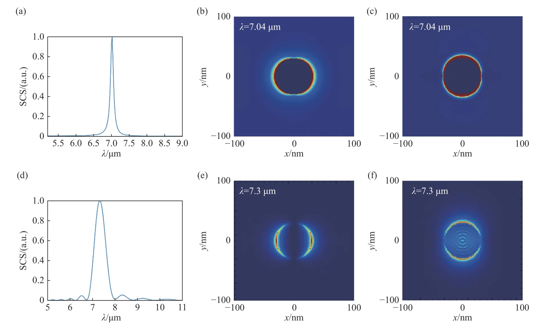
Fig. 4 Comparison of the results from BEM and FDTD. (a) SCS spectrum obtained by BEM; (b) magnetic field distribution obtained by BEM under the resonance wavelength; (c) electric field distribution obtained by BEM under the resonance wavelength; (d) SCS spectrum obtained by FDTD; (e) magnetic field distribution obtained by FDTD under the resonance wavelength; (f) electric field distribution obtained by FDTD under the resonance wavelength图 4 边界元算法与有限时域差分算法结果对比图。(a)边界元获得的SCS谱线;(b)共振波长下边界元获得的磁场分布;(c)共振波长下边界元获得的电场分布;(d)有限时域差分获得的SCS谱线;(e)共振波长下有限时域差分获得的磁场分布;(f)共振波长下有限时域差分获得的电场分布
4.2 Dependence of SCS spectrum on the chemical potential of graphene
One advantage of graphene over other materials is that its chemical potential can be dynamically adjusted by an applied electric field and other methods. Therefore, we calculated the influence of the change of chemical potential on the scattering characteristics of a graphene disk, without changing other parameter settings as shown in Figure 4. The chemical potentialEFwas set as 0.1, 0.15, 0.2 and 0.25 eV respectively. The calculation results are shown in Figure 5(a). It can be seen from the calculation results that, with the increase of chemical potential, the resonance wavelength is blue-shifted, the scattering intensity gradually increases, and the resonance peak width gradually decreases.
According to the reference [17], the relationship between the plasmon resonance frequency and electrochemical potential of graphene is ωp~(EF/D)1/2. Therefore, as the chemical potential of graphene increases, the resonant angular frequency will increase and the resonant wavelength will be blue-shifted. The number of charge carriers and the density of free charges gathered at both ends of the disk will increase with the chemical potential of graphene, leading to stronger scattering field intensity. The spring oscillator model presented in[32, 34] can explain many SPR phenomena. The scattering spectrum and absorption spectrum in the models meet the following linear law:
whereris the parameter related to structure and material, and Γaand Γsare the absorption coefficient and scattering coefficient respectively.
Since the SCS spectrum obtained by calculation is similar to the ACS spectrum, we only use the SCS spectrum to study the properties of graphene structure. By fitting the equations (12) and (13) with the ACS spectrum and SCS spectrum, we can obtain the scattering coefficientГsand the absorption coefficientГa. It is worth noting that since only the equation (13) is used to fit the scattering spectrum to obtain three relevant parameters, we should pay attention to the way of fitting and combine equation(13) with equation (12) in order to obtain accurate results. Ifω=ω0, both the SCS and ACS will be peaks, and the results will be as follows:

From the above two equations,andcan be obtained.Cabs_maxandCsca_maxcan be obtained from the scattering and absorption spectra. Therefore, we can fit the one parameterГsonly through equation (13), and obtain accurate results.
In Fig. 5(b), we show the relationship between the scattering coefficientГsand the chemical potential. It can be seen thatГsincreases with the chemical potential, which further explains the change rule of the scattering intensity. Also as shown in [32], for the narrow-band model structure of graphene in our paper, the scattering coefficient is directly proportional to the square of the charge involved in resonance and inversely proportional to the square of the resonance wavelength. This can also explain the change rule of the scattering coefficient. According to Reference [32], the half peak width of the scattering spectrum is directly proportional to the extinction coefficientГand the square of the wavelengthλ, that is, Δλ~Γ·λ2, where the extinction coefficientГis the sum of the scattering coefficientГsand the absorption coefficientГa. The relationship between the physical quantity Γ·λ2and the chemical potential is given in Figure 5(c). The physical quantity will decrease with the increase of chemical potential, thus explaining the change rule of half peak width.

Fig. 6 Influence of convex shape on SCS spectrum. (a) Relationship between SCS spectrum and convex height; (b) relationship between SCS spectrum and convex width图 6 凸起的形状对SCS谱线的影响。(a)SCS谱线与凸起高度的关系;(b)SCS谱线与凸起宽度的关系
4.3 Scattering spectrum changing with convex shape
In practical use, graphene may exhibit structural deformation due to the reasons mentioned earlier.Therefore, we also considered the influence of nonplanar convex structure on the LSPR of graphene.We calculated a disk-shaped planar graphene structure (as shown in Figure 4) with a bulge in the center and a chemical potential ofEF=0.2 eV. At first,the total width of the bulge was set as 20 nm, and its height was set as 10, 20, 30, and 40 nm respectively.The SCS spectrum results were obtained, as shown in Figure 6(a). We found that, with the increase of the bulge height, the resonance peak moved to the long-wave direction, resulting in a red shift. At the same time, the resonance peak intensity increased.The red shift of the resonance wavelength was mainly caused by two reasons. First, with the increase of the bulge height, the path of charge movement from one end of the graphene structure to the other end became longer[32]. Second, as the charge passed through the bulge, it could only be driven by the component of the electric field of the incident light in the direction of the path. Therefore, the increase of the bulge height led to the decrease of the charge-driving force, thereby slowing down the response of a charge to the incident light field[26]. That is to say, the bulge hindered the movement of the charge. Both reasons led to a longer cyclical movement period of the free charge, a lower resonance frequency and a red shift of the resonance wavelength. On the other hand, the increase of scattering intensity was possibly caused by the increase of the bulge height, which might lead to the increase of charge carriers inside the graphene and the increase of the charges gathering at both ends of the graphene structure to form a stronger scattering field. From this, we inferred that if the height of the bulge was fixed and its width was changed, a similar changing trend could also be generated to cause a resonance red shift and enhanced scattering. Then we did the calculation and obtained the results shown in Figure 6(b). We set the height ash=30 nm and the width changing from 10 nm to 20.5 nm. The calculation results were similar to what we expected, except that the SCS spectrum had no significant change until the bulge width was more than 18 nm.
5 Conclusion
In this paper, the SPR properties of the graphene nanodisk were studied by using the boundary element method. We established the numerical model of the geometrical structure of a graphene nanodisk, wrote a 3D-BEM algorithm based on C++language, and calculated the scattering spectrum of the nanodisk and its electric and magnetic field distributions at resonant wavelength.At first, we compared the results obtained by BEM with those obtained by the commercial software based on FDTD and verified the correctness of our program. Then we calculated the scattering spectra of the graphene disk under different chemical potentials. We found that with the increase of chemical potential, the resonance wavelength was blue-shifted, the scattering intensity increased, and the resonance peak width decreased gradually. Finally, we added a convex structure to the original graphene nanodisk model,and considered the influence of the convex structure on the scattering properties of graphene. Our research will contribute to the understanding of the physical law of graphene LSPR and the influence of surface corrugations on the LSPR phenomenon.
——中文对照版——
1 引 言
当光照射到金属表面,金属内的自由电荷在入射光场的驱动下形成集体震荡,表现出强烈的散射、吸收或者耦合,这个特性称为表面等离子体激元共振(Surface Plasmon Polaritons, SPPs)。SPPs具有很强的局域场增强效应,由于其传导波长比入射光小,因此可以应用于光波导[1]、光刻[2]等领域。当金属尺寸缩小至几十纳米或者几百纳米时,沿表面传导的电磁波将会被束缚在表面,形成局域表面等离子体共振(Localized Surface Plasmonic Resonance, LSPR)。由于LSPR的共振波长、共振强度、散射谱线等能够通过改变纳米结构的材料、形状等因素调节,所以在生物传感[3]、能源[4]、信息[5]等领域被广泛研究和应用。
石墨烯是由碳原子按蜂窝晶格链接而成的单原子层二维晶体[6],是一种良好的LSPR材料,可以实现超强的局域场增强效应,同时损耗较低,此外,石墨烯的性质能够通过化学掺杂或者外加电场等方法进行调节,因而石墨烯可以用于实现外部调制的新型LSPR光学器件[6],在光波导[7–9]、生物传感[10]、超表面[11]、超材料[12,13]、光电器件[14]等光学领域具有广阔的应用前景。石墨烯纳米圆盘是一种常用的石墨烯结构,C.X.Cong等人通过纳米球光刻技术与反应离子刻蚀技术相结合,成功地制备了有序石墨烯纳米盘阵列[15]。Sukosin Thongrattanasiri等人研究了石墨烯纳米圆盘在光学吸收中的应用,展示了一种能够实现100%光学吸收的周期性石墨烯纳米圆盘阵列[16]。Zheyu Fang等人提出了基于石墨烯纳米圆盘的可调节光学吸收器,研究了其吸收特性与纳米盘尺寸、间距以及化学势的关系[17]。Hugen Yan等人研究了石墨烯纳米圆盘的耦合效应,证明了不同的耦合方式会带来不同的电磁响应[18]。Jialong Peng等人报道了基于耦合石墨烯纳米盘的可调太赫兹半波片,采用反射式结构实现了半波片的功能[11]。Lauren Zundel等人利用石墨烯纳米圆盘阵列的等离激元的电调谐特性,实现了亚波长空间分辨率的红外分子传感[19]。Vasilios D. Karanikolas等人研究了石墨烯纳米盘在量子发射极之间的作用,研究表明石墨烯纳米盘的强烈共振能够使量子发射器之间的相互作用距离提高一个数量级[20]。
然而,以上研究全部针对于理想的平面石墨烯。石墨烯作为一种柔性材料,在加工过程中会产生凸起、凹陷、褶皱等非平面的缺陷结构,同时,随着现代微纳加工技术的进步,也可以通过人为拉伸、挤压或者机械振动等方法,来制造具有表面褶皱的三维结构,并可控制它们的尺寸参数[21-23]。这些三维结构对石墨烯的表面等离激元共振也会产生调制作用。Penghong Liu等人研究了楔槽形状的石墨烯波导的SPPs模式,获得了不同模式下的表面等离子体激元传播常数以及局域场分布[8]。Slipchenko等人研究了带波纹的石墨烯层的SPPs反射特性,定量描述了褶皱对反射强度的影响[24]。Shengxuan Xia等人通过正弦型石墨烯层证明了可调节的电磁诱导透明特性[25]。Li Wang等人研究了在软基底上塑造的弯折石墨烯纳米带阵列的LSPR特性,并发现了新的解耦合机制[26]。然而,以上工作全部是二维结构,对于存在三维缺陷结构的非平面石墨烯的研究还鲜有报道。
This sounded like a reasonable idea to all of us kids, so we kept on going with the stories. My mom knew the true story, though. Bobby s mom was a single parent, and she suspected that they just couldn t afford the Easter Bunny.
本论文采用三维边界元算法(three dimensional Boundary Element Method,3D-BEM or BEM),研究了平坦及带凸起石墨烯纳米圆盘的表面等离子体共振特性。相对于其他常用仿真算法,3D-BEM能够将三维物体的计算简化为物体表面场的求解,即将三维计算降低到了二维,能够减小计算机资源的占用,从而提高计算速度。编写了基于C++语言的三维边界元数值计算程序,从计算结果可以看出,中红外波段的入射光能够激发石墨烯结构的表面等离子体共振现象。通过调节石墨烯的电化学势发现,共振波长,散射强度,谱线的半高宽都会发生规律性变化。通过对石墨烯结构加入凸起结构,也会使散射谱线发生移动。本文从电荷运动规律,以及借助弹簧振子模型,对文中的变化规律进行了必要的解释。本文研究将有助于理解石墨烯的LSPR特性,同时也推广了BEM算法的应用范围。
2 三维边界元算法理论
本文考虑的三维空间散射问题如图1所示。在各向同性的自由空间中,存在一个三维的散射物体。无穷远的入射光照射到散射体上。散射体表面S将空间分成两部分,散射体外部区域V2和内部区域V1。散射体的表面外法向量为区域V1和区域V2的折射率、相对介电常数、磁导率分别为n1、ε1、μ1,n2、ε2、μ2。
从经典麦克斯韦方程组出发,结合矢量格林定理,可以推导出以下方程,用以表示整个空间的电场磁场分布情况[27]:


获得了散射体表面上的电场磁场分布之后,再进一步离散化方程(1)和(2),便可以获得空间中任意一点的磁场。然后利用麦克斯韦方程可以计算得到该点的电场,进而获得整个空间的电场磁场分布。之后,可以计算其他物理量,比如散射截面(Scattering Cross Section,SCS)、吸收截面(Absorption Cross Section,ACS)等。
散射截面和吸收截面可以由式(5)和式(6)获得[30]:
其中Ws与Wa为散射功率和吸收功率,其可以选择一个包围散射体的闭合表面Г,借助能流密度(坡印廷矢量)来计算获得:


3 石墨烯纳米圆盘的建模
首先考虑石墨烯纳米圆盘形的结构,其直径为d=60 nm,位于x-y平面内,如图2(a)所示。针对有缺陷的石墨烯结构,考虑石墨烯纳米圆盘中心处有一个凸起,这种凸起型结构可以通过谐振器的机械振动来实现[23],凸起高度为h,如图2(b)所示。定义凸起宽度为高度变为h/exp(1)时的长度,标记为w,则该褶皱石墨烯纳米圆盘在z方向上的坐标可以描述为:

侧面分为两层,每一层分别为116个面元。因此所有网格面元合计共1224个。面元中心点位置及外法向向量如图2(d)(彩图见期刊电子版)所示。针对凸起结构的网格划分是在平整圆盘结构的基础上,沿z轴往凸起结构做投影产生的。
石墨烯的光学参数计算采用文献[32]中的方法。其介电常数可以由下式获得:

其中ε0为真空介电常数,ω为入射光的角频率,σ为石墨烯的电导率,i为虚数单位,t为石墨烯厚度。石墨烯电导率在远红外及太赫兹波段可以表示为[7, 33]:其中e为单位电荷电量,EF为石墨烯化学势,τ为载流子弛豫时间。数值计算程序采用C++语言编写,在上文所述的分面元条件下,程序占用内存大约为1.6 G,普通的个人电脑(配置:i7-8550U,4.0 GHz,8G RAM)计算一个波长点大约需要5 min。整个算法的计算流程如图3所示。
4 仿真结果与分析
4.1 边界元算法与有限时域差分算法的结果对比
为了验证编写的三维边界元程序的正确性,首先计算了石墨烯纳米圆盘在5~11 μm波长范围内的SCS谱线和共振峰位置处的电磁场分布,并将边界元算法获得的结果与基于有限时域差分算法(Finite-Difference Time Domain,FDTD)的商业软 件Lumerical FDTD Solutions的 结 果 做 了 对比。所计算的石墨烯圆盘直径为d=60 nm,化学势为EF=0.25 eV。入射光垂直于圆盘沿−z轴方向正入射,为线偏光,电场偏振方向沿y轴方向。两种算法的归一化SCS谱线分别如图4(a)和4(d)所示。可以看出,在所计算波段内,两种算法都只得到了一个散射共振峰。边界元算法的共振峰位置在7.04 μm,而有限时域差分算法的共振峰位置在7.3 μm,相对误差为3.6%。
图4 (b)~4(c)、4(e)~4(f)分别给出了在共振峰波长下,边界元算法和有限时域差分算法计算出的电场和磁场分布。通过对比可以看到,两种方法获的电场和磁场分布十分相似。对电场而言,光场主要聚集在沿入射光偏振方向(y方向)的两个区域。而磁场分布则与电场垂直。这主要是由于入射光的电场分量使得石墨烯内部的自由电子在电场方向产生集体振荡,形成等离子体共振。因此,图4(a)、4(d)中的共振峰是由于石墨烯的表面等离子体共振造成的散射增强。
4.2 散射谱对石墨烯化学势的依赖关系
石墨烯材料相对于其他材料的一个优势在于,其化学势可以由外加电场等加以动态调节。因此本文计算了化学势的改变对于石墨烯圆盘散射特性的影响,其他参数设置与图4保持一致。化学势EF分别选取0.1、0.15、0.2、0.25 eV,其结果如图5(a)所示。由结果可以看出,随着化学势的增加,共振波长发生蓝移,散射强度逐渐增强,且共振峰的宽度逐渐减小。
通过文献[17]可知,因为石墨烯的等离子体共振频率和电化学势满足以下关系:ωp~(EF/D)1/2。所以,当石墨烯的化学势增加时,共振角频率增加,共振波长发生了蓝移。当石墨烯化学势增加时,载流子的数量增多,聚集在圆片两端的自由电荷密度增加,由此产生的散射场强度会更大,进而增强了散射强度。文献[32, 34]所展示的弹簧振子模型,可以解释很多表面等离子体共振的现象。其中散射谱线与吸收谱线满足以下线型规律:
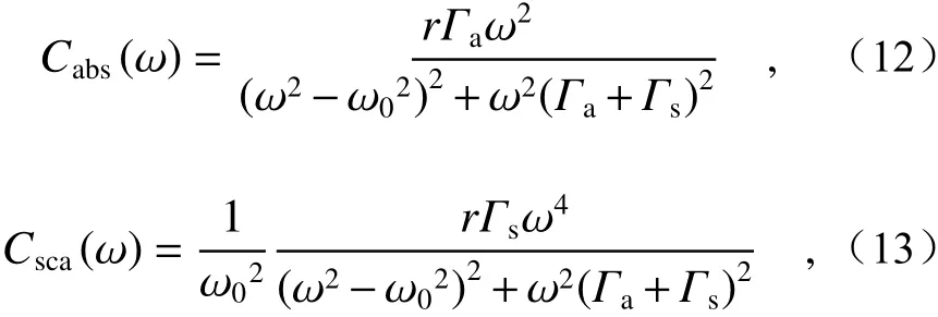
其中r为与结构、材料等有关的参量,Γa与Γs别为吸收系数与散射系数。
由于计算得到的SCS谱线与ACS谱线相似,故本文只采用SCS谱线来研究石墨烯结构性质,通过ACS谱线与SCS谱线来拟合式(12)和(13),可以得到散射系数Γs与 吸收系数Γa。值得注意的是,由于仅使用式(13)拟合散射谱线可获得3个相关参数,需要注意拟合的方式并且结合式(12),才能获得精确的结果。当ω=ω0时,散射、吸收截面均为峰值,结果如下:


图5 (b)展示了散射系数Гs与化学势的关系,可以看出Гs随着化学势的提高而提高,这也进一步解释了散射强度的变化规律。同时文献[32]也表明,对于石墨烯这种窄带模型结构,散射系数同时正比于参与共振的电荷量的平方而反比于共振波长的平方,由此也可以解释散射系数的变化规律。在文献[32]中,散射谱线的半峰宽度Δλ~Γ·λ2,半峰宽度正比于消光系数Г与波长λ的平方,其中消光系数Г是散射系数Гs与吸收系数Гa之和,图5(c)中给出了物理量 Γ ·λ2与化学势的关系,化学势的提高会引起此物理量的降低,这也解释了半峰宽度的变化规律。
4.3 散射谱线随凸起形状的变化
在石墨烯材料的实际使用过程中,由于上文所述的原因,石墨烯会产生结构上的形变,因此本文也考虑了非平面的凸起结构对石墨烯局域等离子体共振的影响。在图4圆盘型平面结构的基础上,计算了中心带有凸起的石墨烯结构,其化学势为EF=0.2 eV。首先设置凸起的总宽度为20 nm,其高度分别为10、20、30、40 nm,其SCS谱线结果如图6(a)所示。可以发现,随着凸起高度的增加,共振峰的位置往长波方向移动,产生红移。同时共振峰的强度随之提高。共振波长红移主要是由两个原因导致的,其一是随着凸起高度的增加,电荷从石墨烯结构的一端运动到另一端的路径变长[32];第二,当电荷经过凸起的时候,入射光的电场只有在路径方向上的分力才会对电荷产生驱动作用。因此当凸起结构的高度增加时,导致电荷驱动力降低,使得电荷对入射光场的响应减缓[26]。也就是说,凸起对电荷运动起到了阻碍作用,这两者同时导致自由电荷作周期性运动的周期变长,共振频率降低,共振波长红移。至于散射强度的增加,分析认为是所设置的凸起变高之后,可能使石墨烯内部的载流子数量增加,聚集在石墨烯结构两端的电荷会更多,散射场会更强,这就导致散射强度的增加。由此也可以预想,如果固定石墨烯凸起的高度不变,而改变石墨烯凸起的宽度,也会产生相似的变化规律,共振红移,散射增强。相关计算结果如图6(b)所示。固定高度h=30 nm,宽度从10 nm变化到20.5 nm,结果与预期相似,不同的是,宽度在18 nm以下时,SCS谱线变化缓慢,而超过18 nm之后,SCS谱线才有明显变化。
5 结 论
本文采用边界元算法研究了石墨烯纳米圆盘的表面等离子体共振特性。针对石墨烯纳米圆盘的几何结构进行数值建模,编写了基于C++语言的三维边界元算法,并计算了纳米圆盘的散射谱和共振波长下的电磁场分布。首先将边界元与基于有限时域差分算法的商业软件做了结果对比,验证程序的正确性。然后计算了石墨烯圆盘在不同化学势下的散射谱线。发现随着化学势的增加,共振波长产生蓝移,散射强度增强,并且共振峰的宽度在逐渐减小。最后,在原石墨烯纳米圆盘模型的基础上,加入了凸起结构,研究了凸起对石墨烯散射性质的影响。本文研究将有助于理解石墨烯表面等离子体局域现象的物理规律以及表面褶皱对该局域现象的影响。
附录:
标量化后的方程如(16)−(21)所示:

其中P1,P2,Q1,Q2分别为:

离散化后的方程分别如(22)−(27)所示:
猜你喜欢
测试技术学报(2021年3期)2021-06-11
广州化工(2020年21期)2020-11-15
石材(2020年6期)2020-08-24
长春师范大学学报(2019年8期)2019-09-10
数学物理学报(2017年1期)2017-06-05
红蜻蜓·低年级(2017年3期)2017-03-30
光学精密工程(2016年1期)2016-11-07
衡阳师范学院学报(2016年3期)2016-07-10
铜业工程(2015年4期)2015-12-29
周口师范学院学报(2015年2期)2015-04-24
