
An ultra-fast C-NOT gate based on electric dipole coupling between nitrogen-vacancy color centers
2021-09-29 09:04ShiShunyangJiWentaoWangYaDuJiangfeng
中国科学技术大学学报 2021年3期
Shi Shunyang, Ji Wentao, Wang Ya*, Du Jiangfeng*
1. Department of Modern Physics, University of Science and Technology of China, Hefei 230026, China;2. Hefei National Laboratory for Physical Sciences at the Microscale, Hefei 230026, China;3. CAS Key Laboratory of Microscale Magnetic Resonance, University of Science and Technology of China, Hefei 230026, China;4. Synergetic Innovation Center of Quantum Information and Quantum Physics, University of Science and Technology of China, Hefei 230026, China
Abstract: Our research proposes a new scheme to build a controlled-NOT(C-NOT) gate between two adjacent nitrogen-vacancy (NV) color centers in diamond, using electric dipole coupling between adjacent NVs and selective resonant laser excitation.The electric dipole coupling between two NVs causes the state dependent energy shift.This allows to apply resonant laser excitation to realize the C-phase gate.Combined with a single qubit operation, C-NOT gate can be implemented quickly.Between two adjacent 10 nm NVs, the C-NOT gate can operate up to 120 ns faster than the traditional magnetic dipole coupling method by 2 magnitudes.In order to reduce the effect of a spontaneous emission,we propose to use a non-resonant cavity to suppress the spontaneous emission.The simulation results show that the C-phase gate fidelity can reach 98.88%.Finally, the scheme is extended to a one-dimensional NV spin chain.
Keywords: nitrogen-vacancy color center;quantum computing;C-NOT gate;1D-spin chain
1 Introduction
Because of the great prospect of the quantum computing and quantum communication, there has always been a desire to implement a scalable, fault-tolerant, coherent, fully controlled quantum system in a physical system[1].Ion traps, superconducting circuits, quantum dots, and solid-state spins are all strong competitors to achieve this goal.The NV color center in diamond, which has the advantages of a long coherence time[2], optical initialization and reading[3], has been the focus of research for a long time, such as the manipulation of NV color center electrons[4], entanglement of electrons with nuclear spin, magnetic detection[5]. Using the hyperfine coupling between NV and a nuclear spin, combined with frequency-selecting microwave and radio frequency pulses, C-NOT operation between the NV electron spin and adjacent nuclear spin has been realized[6]. The long coherence time indicates that there is more time available to perform the quantum operation before the system is decoherent. But it also desires the fast operation, otherwise the advantage of the long coherence time will be offset. So, a fast gate operation scheme is required, and the rapid implementation of the two qubit C-NOT gate is the key in all schemes.
The most used manipulation of the NV color center is to perform single qubit operations via the interaction of the microwave with the magnetic dipole[7-8]. In order to shorten the operating time, the optical holonomic single-qubit gate was proposed[9]. Using the geometric interference of polarized light and NV’s spin-orbit interaction, the full control of NV spin-1 subspace has been realized[9]. However, this is limited to a single NV. As for two qubit operation of two NVs, via bell-state measurement of the two NV’s zero phonon line(ZPL) photons, entanglement is generated between the two NVs over a long distance[10]. But the whole process is inefficient, complex, difficult and not fully coherent. This research extends the optical quantum control from a single-qubit to two qubits, and proposes a scheme that can do C-NOT operation rapidly and efficiently between two adjacent NVs.
The core of the C-NOT gate is a C-phase gate. That is to selectively provideπphase (i.e., multiply-1) for one of the 4 base states(|00〉, |01〉, |10〉, |11〉) of two qubits. The Rabi oscillation between the state and an auxiliary excited state under resonant laser excitation goes through a 2πcycle, which exactly providesπphase for the state. Here we use electric dipole coupling between NVs to remove degeneracy and create a difference in excitation frequency to ensure that only one ground state will be excited and thus experiences a 2πRabi oscillations. Similar methods have precedents in the Rydberg atom system[11-13]. The electric dipole coupling is also used to implement a C-phase gate in the Rydberg atom system, such as the dipole blockade of excitation[13-14].
Spontaneous radiation originates from the interaction between NV’s electric dipole moment and a vacuum fluctuating field. It is not difficult to imagine that there is an electric dipole coupling between two adjacent NVs, like a common magnetic dipole coupling. As long as the distance between two NVs is small enough, the electric dipole coupling is strong enough. The coupling will cause the state mixing and energy level shift, especially the energy level shift is related to their spin state. So if the coupling is strong enough that transitions are no longer degenerate, a resonant laser excitation can be used to excite a specific transition which allows us to build an ultra-fast C-NOT gate.
This paper studies and proposes a new C-NOT gate scheme based on the electric dipole coupling between NVs at low temperatures. It can perform C-NOT operation on two adjacent NVs through microwaves and laser pulses. The operation is extremely fast, which shows that the same coherence time allows the construction of a quantum circuit with greater depth. Secondly, we numerically studied the effectiveness and fidelity of the scheme. Through the analysis of the parameters, an auxiliary method is proposed to improve the fidelity, which is to put the NV color center into the non-resonant optical cavity to suppress the spontaneous radiation. At last, the scheme is extended to a one-dimensional NV spin chain. We believe that this research will lay the foundation for the scalability and complete the control of the NV system.
2 Basic theory
According to the optical transition characteristics of the NV color center, transitions are allowed between the excited state |Ex〉, |Ey〉 and the ground state |ms=0〉. Transitions are also allowed between the excited state |E1〉, |E2〉, |A1〉, |A2〉 and the ground state |ms=±1〉, and the rest are forbidden[15](Figure 1(a)). First, we use two NV color centers that are very close(about 10 nm), and use their respective |Ey〉, |ms=0〉(logical 0), |ms=-1〉(logical 1) to construct a C-NOT gate. Each NV color center can be regarded as a three-level system(Figure 1(b)). We use |e〉 to represent |Ey〉, |0〉 to represent |ms=0〉, and |1〉 to represent |ms=-1〉. The solid arrow represents the allowed optical transition. It can be seen that transitions between |0〉 and |e〉 are allowed, and transitions between |1〉 and |e〉 are prohibited. This means that the electric dipole operatordexpands under the base vector: 〈e|d|0〉≠0 and 〈e|d|1〉=0.
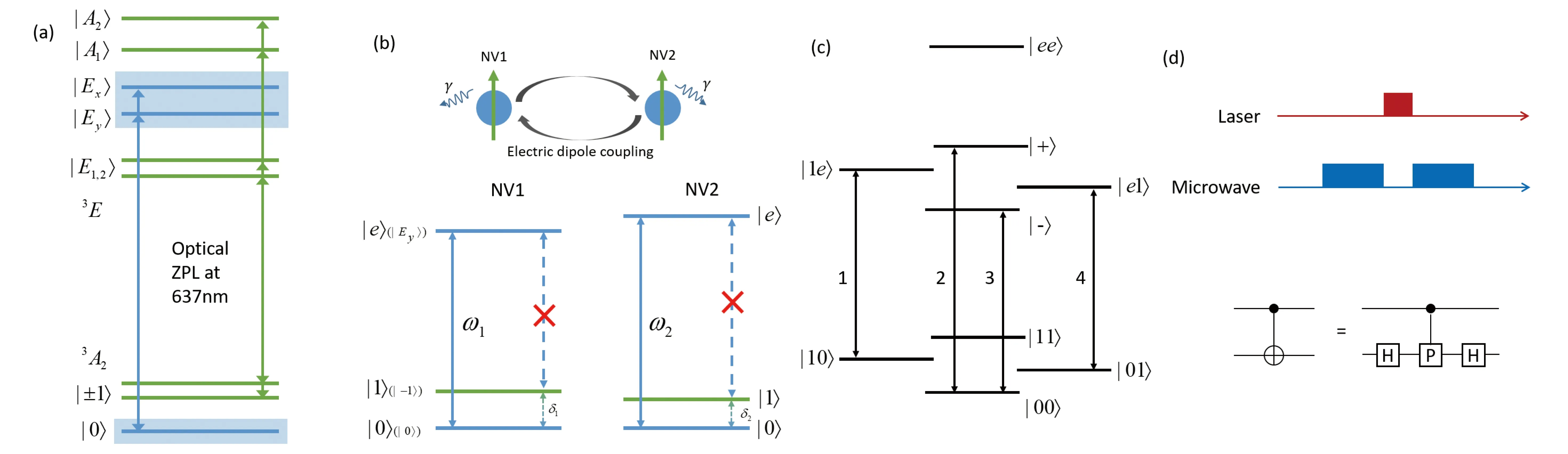
Figure 1. (a)NV color center energy level structure and transition properties.(b)Each NV can be simplied into a three-level system. There is a transition channel between |0〉 and |e〉, and transition between |1〉 and |e〉 is forbidden.(c)The |+〉 and |-〉 in the gure respectively represent the high and low energy state of mixed states between |0e〉 and |e0〉. There are four transition channels with dierent frequencies.(d)The pulse sequence forming the C-NOT gate: two hadamard gates combined with a C-phase gate.
On this basis, the electric dipole coupling term in the Hamiltonian is[16-17]
(1)
Hdd=ћν(|00〉〈ee|+|ee〉〈00|+|0e〉〈e0|+|e0〉〈0e|)
(2)
Here assume thatd1=〈e|d1|0〉 andd2=〈e|d2|0〉 are real. This form indicates that energy level shift and state mixing only occur in the states related to |e〉 and |0〉, but it does not affect the rest of the states. In Eq. (2),

(3)
Using the relationship between a spontaneous emission and a transition electric dipole, it can be estimated that when two NV color centers are separated by about 10 nm,ν=2π×414 MHz.The Hamiltonian of the two NVs themselves is
H0=HNV1+HNV2=ћω1|e〉1〈e|+ћδ1|1〉1〈1|+
ћω2|e〉2〈e|+ћδ2|1〉2〈1|
(4)
The ground state |0〉 and |1〉 have an interval of 2.87 GHz due to the zero-field splitting, and can be adjusted by a magnetic field, which are represented byδ1andδ2. The angular frequency of the transition between |0〉 and |e〉 can be adjusted by stress[19]or the electric field[20], denoted byω1andω2respectively. The overall Hamiltonian with no external field applied is
Htotal=H0+Hdd
(5)
Since theHddcontributes non-diagonal items |00〉〈ee| and |0e〉〈e0|, the linear superposition states of |00〉 and |ee〉, and the linear superposition states of |0e〉 and |e0〉 form new four eigenstates. The resulting energy level diagram is shown in Figure 1(c). Due to the large energy gap, the state mixing between |00〉 and |ee〉 can be safely ignored andE|00〉≈0,E|ee〉≈ω1+ω2. After calculation:
(6)
whereα=ω2-ω1. It can be seen that the role of the electric dipole couplingνis to make the energy levels more separated from each other. The arrow in Figure 1(c) indicates there are 4 allowed transitions.
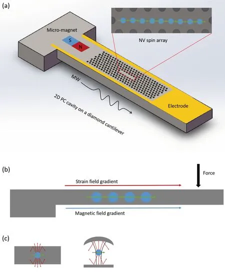
Figure 2. (a)Experimental conception: A two-dimensional photonic crystal cavity is machined on the diamond cantilever, and the NV array is placed in it. Metal electrodes are attached to the top of the beam, and the stress can be controlled by an external electric field. The magnet provides a gradient magnetic field. The cantilever will be placed in a radiating structure to receive microwave pulses.(b)Magnetic field gradient and stress gradient.(c)The schematic diagram of the photonic crystal cavity(left) and the Fabry-Perot cavity(right) respectively. For a dipole radiation source in a cavity, the photonic crystal cavity can confine most of the radiation, while the Fabry-Perot cavity allows most of the radiation to escape.
Based on this new energy level structure, the resonant excitation is explored to realize the desired fast C-phase gate. The key idea is to achieve a 2πoptical gate of one specific transition while leaving the other transitions unaffected. For example, A 2πoptical Rabi oscillation between |01〉 and |e1〉, will make |01〉 become -|01〉 and the other three states unchanged. This ultra-fast C-phase gate, can be combined with a microwave single-qubit operation to form a C-NOT gate (Figure 1(d)). The laser drive Hamiltonian is
Hdrive=-d·E=

(7)
ωis the laser angular frequency, here letω=ω1and consider thatg1=g2=g. Here the transition 4 is taken as an example to show the fast C-phase operation. When the coupling strength isg/2π≈50 MHz, the C-phase operation takes 20 ns. Compared with the scheme using the magnetic dipole coupling between NVs(coupling strength is about 100 kHz when the interval is 8 nm), whose phase accumulation takes about 10 μs to realize the C-phase gate[21], operation speed of our scheme is two orders of magnitude faster.

The required individual control of each NV center can be realized by applying a gradient magnetic field.For a reported magnetic gradient of 1 MT·m-1[23], 10 nm separation between two NVs have a magnetic field difference of 100 Gs, corresponding to a frequency difference of 280 MHz. This means a Hardmard gate can be implemented in about 50 ns. The execution time of the entire C-NOT gate is about 120 ns (about 10 μs in the traditional scheme). The execution time is 2 orders of magnitude smaller than the coherence time.
3 Parametric analysis
In this part, the factors affecting the fidelity of the operation is analysed. First, it is necessary to ensure that the resonance laser only excites the Rabi oscillation of the transition 4, and leave the transitions 1, 2, 3 unaffected. This requires the transition 4 to be separated in frequency from others, that is
Δ4,1≫g,Δ4,3≫g
(8)
gis the coupling strength between the light field and the NV color center.Δ4,1,Δ4,3represents the absolute value of the frequency difference between transition 4 and transition 1, 3. For the former case, the stress or electric field can be used. For the latter case, the electric dipole couplingνshould be as large as possible, andΔ4,1=αshould not be too large. Note that:
(9)
g≫γ
(10)
The larger theg, the smaller the C-phase gate operation time 2π/g. Combining the above two points, it can be found that the coupling intensitygcannot be too large or too small. The spontaneous radiation rateγsets a lower limit, and the interval between transition peaksΔ4,3,Δ4,1sets an upper limit.
To reduce the lower limit, here we explore the Purcell effect of optical cavity. Many experiments have used cavities to control the spontaneous emission, such as using superconducting microwave cavities to increase the relaxation rate of solid spins[25], enhancing the spontaneous emission of Rydberg atoms[26]. The optical cavity can be used to enhance the spontaneous radiation at resonance[27,28], and to suppress spontaneous radiation at non-resonance[29,30]. In fact, the excited state lifetime of the NV color center in the nano-diamond can reach 21 ns[31], which is longer than 12 ns in the bulk diamond, which shows that extending the lifetime is feasible.
According to the purcell effect[32], when the resonance wavelength of the optical cavity is equal to the zero phonon line (ZPL) of the NV color center, the ZPL of the NV color center will be enhanced. When the cavity resonance wavelength is shifted away from the optical resonance spectrum of NV, the spontaneous radiation will be suppressed. Regardless of enhancement or suppression, only part of radiation which enters the optical cavity in the correct direction can be affected. The electric dipole radiation occupies the azimuth angle of 8π/3 in the whole space. We hope that as much light energy enters the cavity as possible, and then be suppressed, so a 2D photonic crystal cavity is chosen (Figure 2(a)(b)). The refractive index of the diamond is 2.42, and the probability that a spontaneous radiation escapes from the cavity without being bound by total reflection isPleaky=0.134. This means that under ideal conditions, all parts in the cavity can be suppressed and the spontaneous radiation rate is reduced to 0.134 times of the original. The lifetime can be extended to 7.5 times of the original. The 2D photonic cavity has outstanding effect compared with other kinds of optical cavity, such as the Fabry-Perot cavity (FP cavity). The solid angle that can enter the cavity mode is extremely small, and a large amount of radiation directly escapes out of the cavity, and the suppression is almost negligible (Figure 2(c)).
4 Numerical simulation
The numerical simulation is used to verify the effectiveness of the entire scheme under the theory of part 2. The simulation ignores the imperfections of devices and microwave operations, and takes into account spontaneous emission, decoherence and unwanted non-resonant excitation, which are dominant error sources in the optical control. We first adopt ideal parameters, assuming that the extended lifetime of the NV color center is 60 ns, and the distance between two NVs is 5 nm, corresponding toν=2π×3.312 GHz. The result is shown in Figure 3(a). The process fidelity is around 98%, which proves that the experimental sequence does implement a C-NOT operation.

Figure 3. (a)The tomography simulation results of the C-NOT gate show that the probability distribution of the final state. It is obtained after the same pulse sequence in the four initial states respectively, which shows that the scheme indeed constitutes a C-NOT gate.(b),(c)With 10 nm and 8 nm interval respectively, the fidelity of the C-NOT changes with the coupling intensity g.(d)With three different coupling intensities, the simulated C-phase fidelity decreases as the distance increases.
Secondly, we consider the effect of the optical control strengthgby adjusting it in a range ofΔ4,1,Δ4,3≫g≫γ. Sincegonly involves the C-phase step, only the fidelity of the C-phase gate is simulated. Set the initial state |ψ0〉=0.5(|01〉+|10〉+|00〉+|11〉). The theoretical target state is |ψtarget〉=0.5(-|01〉+|10〉+|00〉+|11〉). The parameters and results are shown in Figures 3(b), 3(c). When the two NV color centers are separated by 10 nm and 8 nm, the maximum fidelity is 98.26% and 98.88% respectively. The smaller the distance, the stronger the electric dipole coupling. So with the weaker off-resonance excitation, higher fidelity can be reached. Asgincreases, the fidelity curve first rises rapidly and then falls. Whengis too small, the spontaneous radiation will be dominant and reduces the fidelity. Whengis too large, the laser will non-resonantly excite unwanted transitions 1, 2, 3. But the impair to fidelity is moderate. Further simulation shows that if the lifetime is prolonged 10 times (about 120 ns), the fidelity can reach 99.3% when the interval is 8 nm.
Finally, we consider the impact of the coupling strengthνbetween two NVs. The parameters and results are shown in Figure 3(d). The coupling strength decreases with the inverse cubic of the distance. The increase of the interval |r12| leads to the decrease ofν, which in turn leads to the decrease ofΔ4,3. In this situation the fidelity of the C-phase gate decreases due to the effect of the non-resonant excitation of other transitions. So the larger the optical control strengthg, the faster the fidelity decreases. At the same time, the simulation shows that as long asgis not particularly large, there is a slower-decreasing platform area before the rapid fall. When the interval is expanded from 5 nm to 15 nm, the fidelity is still higher than 95%.
5 Scalability
The aforementioned C-NOT gate scheme can be implemented in the case of 2 NVs. Naturally, it is desire to expand from 2 adjacent NV color centers to multiple NVs in a scalable way. Here we consider the C-NOT operation between any NViand NVi+1in a one-dimensional NV spin chain. In this case, the electric dipole coupling between NVi+2and NVi+1, NVi-1and NViwill affect the desired operation between NViand NVi+1. For example, the C-NOT operation between NV2and NV3requires a resonant excitation of the transition between |01〉2,3and |e1〉2,3, however, the electric dipole coupling between NV1and NV2, will induce a NV1’s state dependent frequency shift as shown in Figure 4(a). Undoubtedly this will greatly impair the fidelity.

Figure 4. (a)The state of NV1 will affect the transition frequency of NV2 and NV3.(b)As long as one of NVi-1 and NVi+2 is in |1〉, C-NOT operation between NVi and NVi+1 can be completed.(c)SWAP gate, consists of 3 C-NOT gate.(d)With redundant NV color centers, the SWAP-C-NOT-SWAP operation sequence can be used to implement a C-NOT operation and avoid the impair of additional electric dipole coupling.
To overcome this shortcoming, we consider a spin-chain configuration as shown in Figure 4(d). Some NV color centers are used as redundancy to shield the unwanted electric dipole coupling(the second nearest neighbour coupling is ignored). Let the odd-numbered NV in the chain be the redundant auxiliary NV, all initialized to |1〉. And the even-numbered NV color center used for calculation, which can be in any state. We use NVs in |1〉 as a shield because the energy shift only involves |0e〉 and |e0〉. If C-NOT gate between NViand NVi+1is being operated, at least one of NVi-1and NVi+2must be in |1〉, as shown in Figure 4(b). Due to symmetry, resonantly exciting transition 1(ω=ω2) can also achieve the goal. So there are two C-NOT schemes between NViand NVi+1, one is to resonantly excite NVi, the other is to resonantly excite NVi+1(with slightly different single-qubit operations). These two schemes can use either NVior NVi+1as the control qubit. When NVi-1is in |1〉, C-NOT can be realized by exciting NVi. When NVi+2is in |1〉, C-NOT can be realized by exciting NVi+1. This enables us to do the SWAP gate.
In summary, the one-dimensional NV spin chain can be used as an extension scheme. For example, we want to operate C-NOT gates for NV2and NV4, shown in Figure 4(d). Suppose the initial state of NV2and NV4is |φ2〉=α|0〉+β|1〉, |φ4〉=|0〉. Step 1 is to exchange NV3and NV4with the SWAP gate, then |φ4〉=|1〉, |φ3〉=|0〉. Step 2 is to perform C-NOT operations on NV2and NV3, after the operation |φ2,3〉=α|00〉+β|11〉, NV2and NV3are entangled. Step 3 is to use the SWAP gate to exchange the states of NV3and NV4. After the exchange, NV2and NV4produce entanglement |φ2,4〉=α|00〉+β|11〉. Note that in Steps 1 and 3, the SWAP gate is composed of 3 C-NOT gates[33], as shown in Figure 4(c). Because NV5on the right side of NV4is on |1〉 and the NV2on the left side of NV3is not in |1〉, so it is only feasible to implement these 3 C-NOT with a scheme to excite NV4.
This scheme introduces redundant qubits to avoid the influence of the adjacent electric dipole coupling, but also reduces the NV’s utilization to half. At the same time, a C-NOT operation must be combined with two SWAP operations, which requires a total of 7 C-NOT. So it is best to use a large gradient magnetic field to implement rapid hard pulses.
The NV color center array separated by 1 μm from each other[34]and silicon-vacancy color center separated by 500 nm[35]have been realized. The NV array with a spacing of 40 nm with a positioning accuracy of 10 nm has been realized[36]. Although it has not yet reached an array with an interval of 10 nm, with the advancement of micro-nano processing technology, we believe that this solution can be implemented in experiments in the future.
6 Conclusions
In summary, this study designed a C-NOT gate scheme based on the electric dipole coupling between adjacent NV color centers. The advantage is that the C-phase operation is very fast. Combined with a dynamically corrected gate(DCGs) that can greatly extend the coherence time and strong gradient magnetic fields, the execution time of C-NOT gates can be compressed to the order of hundreds of nanoseconds, which can be used to construct quantum circuits with depths of thousands. And the fidelity of the C-phase gate can be improved by putting the NV color center into the non-resonant optical cavity. It is assumed that the lifetime can be extended by 5 times. Based on this, a series of numerical simulations verified the effectiveness of the entire pulse sequence, and calculated that the fidelity of the C-phase operation between two NV color centers with an interval of 8 nm can reach 98.88%. Then we simulated the trend of decreasing fidelity as the distance between two NVs increases. Finally, we exemplified how to extend the scheme to a one-dimensional NV spin chain. We believe that this kind of C-NOT gate based on the electric dipole coupling can be extended to other systems and has great potential for improvement, making this solution a cornerstone for quantum networks.
Acknowledgments
This work is supported by National Key Research and Development Program of China (Nos. 2018YFA0306600, 2017YFA0305000), National Natural Science Foundation of China (Item Numbers: 11775209, 81788101, 11761131011), Anhui Quantum Information Technology Leading Project (Item Number: AHY050000), Fundamental Research Funds for the Central Universities and USTC Research Funds of the Double First-Class Initiative.
Conflictofinterest
The authors declare no conflict of interest.
Authorinformation
ShiShunyangis currently a graduate student under the tutelage of Prof. Wang Ya at University of Science and Technology of China. His research interests focus on quantum information and quantum computation.
WangYais a professor at University of Science and Technology of China (USTC). He received the PhD degree in science from USTC in 2012, and was awarded the 2012 Dean’s Excellent Scholarship of the Chinese Academy of Sciences. From 2012 to 2016, he did post-doctoral research at University of Stuttgart, Germany. In 2016, he joined USTC. He mainly engaged in experimental research on solid-state quantum devices based on solid point defects and quantum computing applications. The main directions include 1) experimental research on the preparation of high-performance diamond quantum chips and quantum probes; 2) experimental research on spin-based quantum computing networks. Related research results were published inNature,NaturePhotonics,NatureNanotechnology,NatureCommunications,Scienceadvances,PhysicalReviewLetters,PhysicalReviewApplied,ACSNanoand other academic journals, have been cited more than 1800 times (data from Google Scholar).
DuJiangfeng(corresponding author) is an academician of the Chinese Academy of Sciences, a professor of the University of Science and Technology of China, a distinguished professor of the Yangtze River Scholars of the Ministry of Education, a winner of the National Science Fund for Outstanding Youth, a chief scientist of a major national scientific research project, and a member of the first batch of National Ten Thousand Talents Program “Science and Technology Innovation Leaders” , a national-level candidate for the New Century Talents Project. He mainly engaged in experimental research on quantum physics and its applications. He innovatively developed quantum physics experimental technologies such as spin quantum control and dynamics decoupling, combined with the successful development of a series of high-performance magnetic resonance experimental equipment, and improved the sensitivity and resolution of magnetic resonance detection to the international leading level. New applications of quantum physics such as quantum computing have achieved research results with important international influence. He has published more than 200 papers in international high-level academic journals includingScience,Nature,PhysicalReviewLetterandNature-branded sister journals.

- 中国科学技术大学学报的其它文章
- A literature review of corporate green innovation behavior from the perspective of peer effect and prospect: An integrated theoretical framework
- An end-to-end multitask method with two targets for high-frequency price movement prediction
- Hyperplane arrangement complement with top degree Betti number being small
- Riemann-Hilbert approach for a mixed coupled nonlinear Schrödinger equations and its soliton solutions
- A hybrid HWENO-based method of lines transpose approach for Vlasov simulations
- Subgroup analysis for multi-response regression