Growth mechanisms of Ag and Cu nanodendrites via Galvanic replacement reactions
Jialu Chen,Jemima J.Davies,Alister S.Goodfellow,Sarah M.D.Hall,Helena G.Lancaster,Xinyu Liu,Cameron J.Rhodes,Wuzong Zhou
School of Chemistry,University of St Andrews,St Andrews,KY16 9ST,UK
Keywords:Silver nanodendrite Copper nanodendrite Electron microscopy Stacking fault Crystal growth
ABSTRACT Dendritic silver and copper crystals were produced via Galvanic replacement reactions on zinc and aluminum plates,respectively.The growth orientations of these metals were determined using electron microscopy.The results showed that a fast crystal growth associated with a high concentration of metal cations led to kinetically controlled growth along the <112>axes of the cubic close-packed structures.However,a slow growth rate resulted in thermodynamically controlled growth along the [111] axis.The crystal growth was not found to rely upon the direct deposition of metal cations at crystallographic sites on crystal facets,but instead,hydrated metal cations deposited on the crystal surface to form an amorphous coating layer,followed by the reduction of metal cations and crystallization at the crystal/coating interface.Twin defects and stacking faults were often observed across the whole particle and commonly observed 1/3{422} diffraction spots were explained by stacking faults rather than by the possible presence of any superstructures.The present work offers evidences to claim that both the crystal growth rate and Coulomb interaction between negatively charged crystal surface and metal cations play an important role in the formation of metal dendrites in replacement reactions.
1.Introduction
Metal nanostructures have been extensively studied due to their optical,catalytic and electrochemical properties.Amongst them,nanostructures of group 11 transition metals (Cu,Ag,Au) have attracted significant interest as they are extensively used as functional materials;e.g.catalysts [1-4] and a surface enhanced Raman scattering substrate[5].In addition to 0-dimensional(0D)nanoparticles,many morphologies of 1D and 2D nanoscale metals,such as nanowires,nanosheets,nanoprisms and nanodendrites [6-9],have been fabricated.Among them,nanodendritic particles are particularly interesting.They have overall sizes on the micrometer scale,but local crystal sizes on the nanometer scale with physico-chemical properties that depend on growth orientations and morphology.
Several methods have been developed to synthesize silver nanodendrites.One is a template assisted method where either polymer materials or Raney nickel is used as a template to tailor the size and shape of the dendrites [10,11].Another method is template-free direct growth,such as aging a Ag salt with a reductant [12].Besides these,electrodeposition and electroless metal deposition have also been applied[13-15].The simplest method that has been used is a Galvanic replacement reaction (GRR) between silver nitrate and a sacrificial metal such as zinc,tin or magnesium [16-18].Compared with other methods where additives are applied,this method is facile,quick and environmentally friendly.
On the other hand,the growth mechanisms of the dendritic structures via GRR are yet to be fully understood.Several growth mechanisms have been previously proposed for the growth of dendritic structures.One of them is diffusion limited aggregation (DLA) [19,20],which has been commonly used to explain the formation of fractal patterns.However,DLAs are based upon computer simulation with little physical input.In other words,there is no strong inter-particle interaction under consideration,and the particles undergoing aggregation in a random walk are assumed to be the same as the building units of the final dendrites.The naturally occurring dendritic structures may have“a spooky resemblance with the computer generated DLA clusters”[21];however,DLA cannot offer explanations to the highly selective growth directions observed in dendritic growth.For example,the formation of snowflake-like α-Fe2O3nanodendrites via hydrolysis of ferricyanide was found to be controlled by Coulombic forces between positive sites at crystal surfaces and[Fe(CN)6]3-anions,leading to the crystal growth along some particular directions[22].
Another proposed mechanism is the twin plane re-entrant edge(TPRE)mechanism[23-25].In this theory,the existence of at least two twin planes in a metallic structure is the essential factor for continual propagation in the <112>directions.Twinning in a[111]direction can produce a re-entrant angle of 141°and a ridge angle of 219°.If there are more than two twin planes and nucleation preferably takes place in the re-entrant angles,the dendrites would show preference for the growth in the <112>directions:however,experimental data often does not support these hypotheses.
In the present work,the formation mechanisms of these metal nanodendrites are investigated by microstructural analysis of Ag and Cu nanodendrites formed via a GRR using scanning electron microscopy(SEM) and high resolution transmission electron microscopy (HRTEM).The experimental results indicate that Coulomb interaction between the charged crystal surface and metal cations,the crystallization of an interfacial amorphous layer,and the growth speed play important roles in the formation of nanodendrites.The results may shed light on dendrite formation of other metallic and non-metallic materials.
2.Experimental
2.1.Growth of Ag dendrites
Silver dendrites were synthesized using a simple GRR method at room temperature.Typically,AgNO3(0.3397 g) was dissolved in distilled water(10 mL,200 mM).A Zn plate(1×1 cm2)was washed using diluted hydrochloric acid and then rinsed with distilled water three times.After being dried by flowing nitrogen gas,the zinc plate was immersed in the AgNO3solution for 10 s.Silver dendrites were produced on the surface of zinc plate.The zinc plate was washed with distilled water three times and dried in oven at 50°C.The Ag particles were then collected using a spatula.To test the effect of crystal growth speed on the growth direction,different concentrations of AgNO3and reaction time were attempted,i.e.,50 mM,1 min;10 mM,3 min;5 mM,3 min;2 mM,16 min,etc.
2.2.Growth of Cu dendrites
Copper dendrites were synthesized via GRR between CuSO4and Al foil at room temperature.Specifically,an Al foil(1×1 cm2)was cleaned using ethanol and distilled water,and immersed in a solution(2 mL) of CuSO4(50 mM) and HCl (100 mM).The addition of HCl was mainly to prevent the formation of an Al2O3barrier on the Al plate and reduce the Cu crystal growth rate.Red copper metallic particles formed on the Al plate in a few minutes with effervescence.After 1 h,the Al plate was taken out,washed with ethanol and distilled water and dried in vacuo.
Different concentrations of CuSO4(10,30,50,100 and 200 mM),pH values of the solution(4.46,1.67,1.35 and 1.15 with 0,50,100 and 150 mM of HCl,respectively),reaction times(10 s,30 s,60 s,120 s,1 h)and reaction temperatures (4,21 and 35°C) were attempted in order to investigate the impact of these conditions upon morphologies of Cu deposits.
2.3.Specimen characterization
Powder X-ray diffraction (XRD) was performed on a PANalytical Empyrean diffractometer using Cu Kα radiation.The compositions of the specimens were examined using energy dispersive X-ray spectroscopy(EDX) on an Oxford Instruments INCA ENERGY system.SEM images were recorded using a JEOL JSM-5600 or a JEOL JSM-7600F fieldemission gun (FEG) electron microscope operating at 5 kV.TEM images and selected area electron diffraction (SAED) patterns were recorded on a JEOL JEM-2011 electron microscope fitted with a LaB6electron gun,and Titan Themis S/TEM with a FEG,both operating at an accelerating voltage of 200 kV.To prepare a sample for TEM,the dendrite product was gently ground in acetone with a pestle and mortar.One drop of the suspension was deposited onto a copper grid with a thin holey carbon film.The grid was fixed into a double tilt specimen holder for the TEM observation.The TEM images were recorded using a Gatan 794 CCD camera(in JEM-2011) and FEICeta 16 M CMOS camera(in Titan).
3.Results and discussion
3.1.Silver nanodendrites
3.1.1.Fern leaf-like silver dendrites
Silver nanodendrites were produced via GRR:2Ag+(aq)+Zn(s)→2Ag(s)+Zn2+(aq)in a 200 mM aqueous solution of AgNO3,which was very fast due to a large difference in standard electrode potentials of Zn2+→Zn(-0.7618 V)and Ag+→Ag(+0.7996 V).
The powder XRD pattern of the product can be indexed onto facecentered cubic (fcc) structure with the unit cell parameter a4.1040 Å(Fig.S1,in the Supporting Information,SI).It is noted that the relative intensity of the(111)peak is significantly higher than that from normal silver powder.In addition,a few very weak peaks are indexed onto hexagonal ZnO structure,indicating that some ZnO nanocrystallites left on the Zn plate.
The dendritic morphology of the silver particles was observed from SEM images (Fig.1).Some ZnO nanocrystals were also observed,and their chemical composition was confirmed by EDX,which was consistent with the XRD result.The typical dendritic particles were flat as revealed by a series of SEM images of the same particle through tilting(Fig.S2,in the SI),and contained a primary trunk with two rows of parallel secondary branches developed on both sides,60°apart from the trunk(Fig.1a).The same growth manner was adopted by two rows of tertiary branches that developed on each side of the secondary branch (Fig.1b and c).
From SEM images of Ag nanodendrites on the Zn plate,we are able to examine the Ag/Zn interface where the trunks of the Ag nanodendrites were connected to the Zn plate(Fig.1b).In these backscattered electron SEM images,Ag shows brighter contrast than Zn,because Ag has a larger atomic number,having a larger power to generate backscattered electrons.When looking closely at the Ag/Zn interface of a dendrite on Zn(Fig.1c),it is observed that the dendrite has a root,40 nm in length,with no secondary branches,inserting in the Zn plate.This implies that,at beginning,the silver nanocrystal grew into and eroded the Zn plate.At this stage,the active site of the crystal growth was the Ag/Zn interface in question and the insertion of the root into the Zn plate ensured a constant connection of the two metals during the replacement reaction.
On the other hand,when the Ag crystal grew out from the Zn surface,the active site of crystal growth was the top tip of the nanorod (later to become the primary trunk of a dendrite),and it was possible to develop secondary branches on the trunk.A counterexample is the growth of silicon nanowires on Au catalytic nanoparticles,where the growth sites remain at the Si/Au interface.Therefore,each nanowire has a uniform diameter as controlled by the Au particle size and no branches are developed[26].
The crystal structure and growth direction were investigated using SAED patterns and HRTEM images.Since a single SAED pattern or HRTEM image gives only 2D projected information of a 3D structure,to reveal the crystal growth direction,that direction must be perpendicular to the electron beam.This can be achieved by titling the sample until the longest projected length of the particle is observed [27].A typical electron microscopic analysis is shown in Fig.2.
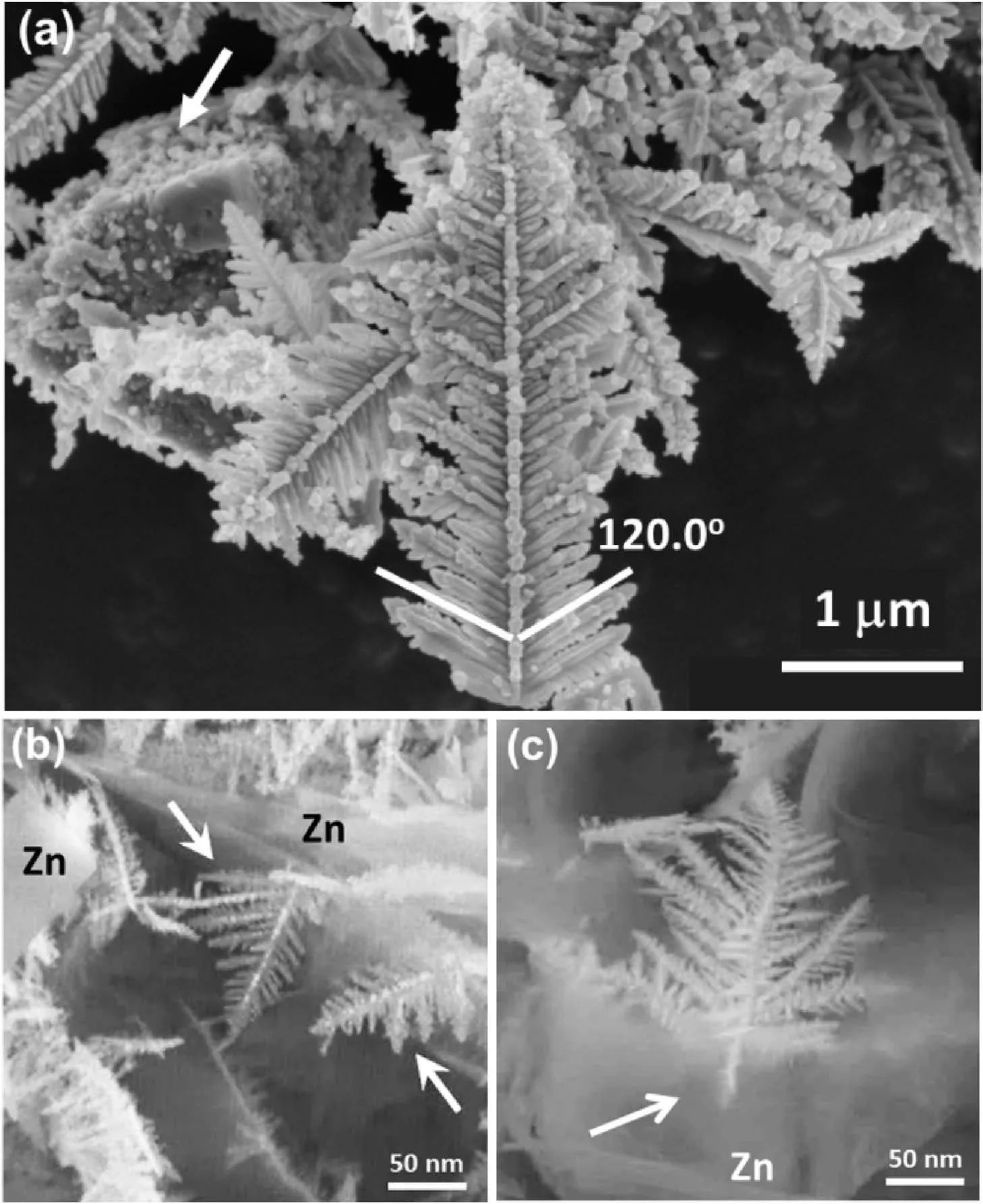
Fig.1.SEM images of silver nanodendrites produced in 200 mM of AgNO3.(a)Dendrites removed from the Zn plate.The arrow indicates some nanocrystals of ZnO.(b)Backscattered electron SEM image of Ag nanodendrites(indicated by the arrows)on the zinc plate.(c)Backscattered electron SEM image of a silver nanodendrite with the root (indicated by an arrow) inserted into the zinc plate.
Fig.2a shows a TEM image of a silver dendrite,with a trunk in the middle with two rows of secondary branches on both sides,each of which have two rows of short tertiary branches.Fig.2b shows an enlarged TEM image from a tip of a secondary branch,and the corresponding SAED pattern indexed to the fcc structure of silver with a viewing direction along the [111] axis.It was found that the growth direction of the secondary branch was along[211]and two tertiary branches alongandrespectively.SAED patterns observed from different areas in the dendritic particle confirmed a single crystal property of the particle.Therefore,the growth direction of the trunk is parallel to thezone axis.It may be concluded that the growth directions of the dendritic particle is highly selective to the <211>axes in theplane.Nucleation and growth of branches out of theplane are never observed.The plate-like morphology of the dendritic particles with the dominated exposed surfaces ofandexplains the extraordinarily high intensity of the(111)peak in the XRD pattern(Fig.S1,in the SI).
Fig.2c shows a HRTEM image of a tip of branch viewing down theaxis,confirming a single-crystal state of the particle.However,the surface is covered by an amorphous layer of about 2 nm in thickness,which is a common phenomenon seen in all the particles.It was also observed that the near surface area of the crystal,indicated by a white arrow,had a relatively lower crystallinity.This implies that,during the crystal growth process,silver atoms were not deposited directly on a crystal facet,but joined the interfacial amorphous layer,which underwent crystallization at the crystal/coating interface to fulfill the crystal growth of the dendritic particle.
Two satellite diffraction spots along the <422>directions,often designated1/3{422},which should be systematically absent according to the fcc structure of silver,were observed previously in silver nanodisk and nanoprism,as well as in close-packed structures of other metals.Several models have been proposed to explain these extra diffraction spots.However,most of these models are either too complicated or hypothetical.In some proposed models,the appearance of the1/3{422}diffraction spot was attributed to surface monoatomic steps [28],or single or multiple twin defects [29,30].We expect that the intensity of the extra diffraction spots according to these models would be too low to be visible if the number of defects is very small.A more reliable model is related to stacking faults.Germain et al.attributed the formation of the 3×{422} superlattice to stacking faults,and believed that,because the stacking faults were sub-nanometer in thickness,their reciprocal points were elongated along thedirection [31].As a result,extra diffraction spots might intersect with Ewald sphere,and the1/3{422}reflections were observed in theSAED pattern.However,we cannot see a direct relation between the appearance of the1/3{422}spots and an intersection of the reciprocal lattice with Ewald sphere.The elongated cell dimension along theaxis is not an intrinsic reason for the appearance of the observed extra spots.The1/3{422}diffraction peaks are forbidden in the cubic close-packed (ccp) structure,but not forbidden in the hexagonal close-packed(hcp)structure and hence,their appearance can be attributed to breakdown of thesymmetry of the ccp structure.
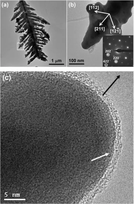
Fig.2.(a)TEM image of a silver nanodendrite formed in 200 mM of AgNO3.(b)Enlarged TEM image from the tip of a secondary branch marked by the square in(a).The inset is the corresponding SAED pattern indexed to the fcc structure of silver.(c)HRTEM image of a tip of a secondary branch.The black arrow shows the growth direction and the white arrow points a surface area with a low crystallinity.
Viewing down the profile of a flat dendritic particle,the SAED patterns revealed a large number of twin defects and stacking faults crossing the particle thickness,e.g.the[111]direction as shown in Fig.S3,in the SI.A perfect ccp structure can be regarded as a regular packing of three identical layers ABCABC(coloured atomic positions with A:blue;B:pink;C:yellow),along theaxis,as shown in Fig.3a.It is obvious that the smallest d-spacing between two adjacent atomic layers along the [211]direction is the d-spacing of the(422)planes,and the1/3(422)diffraction spot is absent.
On the other hand,a hexagonal unit cell can also be drawn for this ccp structure with its(ab)hplane on theplane(Fig.3b)and its c axis along thedirection.The subscripts h and c indicate the hexagonal and cubic unit cells,respectively.In this case,the original (422)cdiffraction spot would transfer to (300)h,and the (100)hand (200)hdiffraction peaks are systematically absent since all three layers along this direction are identical.
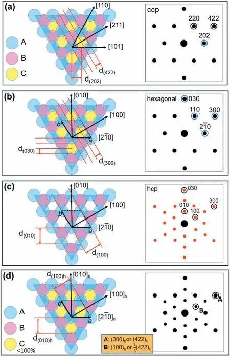
Fig.3.Schematic diagrams of silver crystal structures viewed down the stacking direction and the corresponding SAED patterns.(a) Original ccp structure with ABCABC stacking along the viewing direction of .The A,B,C layers are identical and fully occupied.The SAED pattern is indexed to the fcc unit cell.(b) The same ccp structure as (a)indexed to a hexagonal unit cell.(c) The hcp structure with ABAB stacking along the [001]h direction.The SAED pattern is indexed to the hcp unit cell.(d) A ccp structure with different occupation factors in the layers due to stacking faults.The SAED pattern is indexed to both the fcc and hexagonal unit cells.
If one removes all the C layers,the structure is compressed along thedirection,an hcp structure can be created(Fig.3c).The unit cell dimensions of a and b are exactly the same as that in Fig.3b.However,because the C layers are missing,the(100)hspot is not absent.
Turning back to the ccp structure,it is seen that if there are some stacking faults and twin defects along the view direction,the regular ordering of ABCABC is broken.The numbers of A,B and C layers are no longer identical.Fig.3d shows an example model with A and B layers fully occupied,but the C layers are not fully occupied.The smallest period along the[211]cdirection is three times of the d-spacing of(422)c.In other words,the originally absent1/3(422)cor(100)hdiffraction spot will appear.
On the other hand,when a crystal consists of two components,the observed SAED patterns can be regarded as a combined consequence of diffraction patterns from these two components[32].Stacking faults in a silver crystal can be treated as a disordered stacking of the ccp and hcp components on the directions ofand [001]h,respectively.Therefore,the observed SAED pattern shown in Fig.2b can be resulted from a combination of theand[001]hdiffraction patterns(Fig.S4 in the SI).
3.1.2.King Mace-like silver dendrites
The selective growth direction of <211>could be attributed to a high speed of growth corresponding to the high concentration of AgNO3(200 mM),governed by a kinetic factor.In this case,the crystal growth rate is proportional to the surface attachment energy,Es,which is inversely proportional to the inter-planar distance along the growth direction.The Esvalue on(422)is much larger than those on other principal facets,such as (111),(200) and (220),etc.Therefore,in conditions favouring a fast growth,the[211]direction is the preferred growth direction.In previous work of fabrication of silicon nanowires,it was found the direction of growth was along the [211] axis of the fcc Si structure when the precursor,silane,was supplied at a high rate.When rate of precursor supply was low,the growth direction turned to the[111]axis,changing from a kinetically controlled process to being under thermodynamic control[33].
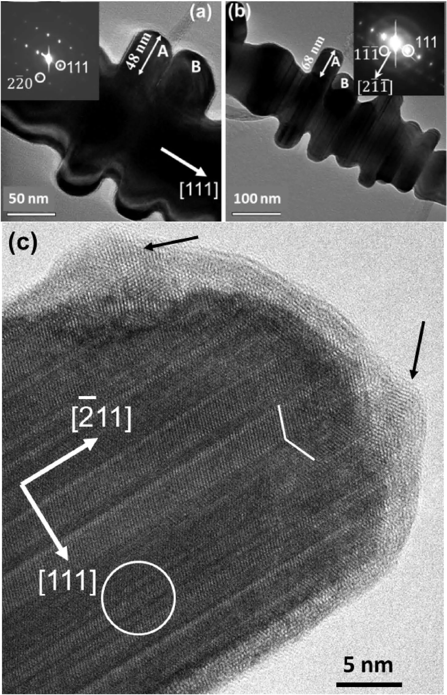
Fig.4.(a,b) TEM images and the corresponding SAED patterns of a silver nanodendrite produced when AgNO3 concentration was 10 mM with a reaction time of 3 min.The image in(b)was recorded after tilting from (a) around the long axis of the trunk until the length of branch“A”showed the longest in projection.(c)HRTEM image of a tip of a secondary branch.The black arrows indicate partial crystallization of the surface amorphous layer.The broken line indicates a twin defect and the circle indicates an area with many stacking faults.
In the present work,several low concentrations of AgNO3were used in order to reduce the crystal growth rate.In a 2 mM AgNO3solution,only spherical nanocrystallites of silver were observed from the product after reaction of 16 min.In a 50 mM AgNO3solution,the Ag dendrite product was similar to that from 200 mM AgNO3.When the concentration of AgNO3was reduced to 10 mM or 5 mM,some dendritic particles appeared with a change of the angle between the primary trunk and the secondary branches from 60°to 90°(Fig.S5,in the SI).Unlike the fern leaf-like particles with discrete branching at regular intervals,some particles in this sample contain secondary branches in the same row connected each other to form a wing.A slow growth rate leads to a thermodynamically more stable state.The secondary branches developed on the trunk along as many as six directions and therefore,the dendrites are not flat,but King Mace-like.It is noted that no tertiary branches were developed in these particles.
To reveal the growth directions of the trunk and branches,the particle under examination was first tilted until the trunk was perpendicular to the electron beam.The observed [111] direction along the trunk is the true growth direction (Fig.4a).A slow growth rate indeed changed the growth direction from[211]to thermodynamically controlled[111].At the same time,a diffraction spot ofwas observed,along a direction perpendicular to the trunk.However,this might not be a growth direction of any branch.Attention was then focused on the secondary branch(marked by A in Fig.4b),tilting the particle again until the long axis of the branch was perpendicular to the electron beam.At this position,thedirection was found to be the true growth direction of the branch A(Fig.4b).It is interesting to note that,during the tilting operation,the length of the adjacent branch (marked B) reduced significantly,indicating that the branches A and B are not parallel to each other.In fact,there are six equivalent <211>directions normal to the [111] axis.Consequently,branches could develop up to six <211>directions on the side surface of the trunk.
Fig.4c is a HRTEM image from a tip of a secondary branch,confirming the growth direction ofand many twin defects and stacking faults along the [111] direction,which is also the growth direction of the trunk.The crystal surface is also covered by a disordered layer with some nanocrystallites developed.The orientations of these nanocrystallites are not the same as the core crystal.The lighter image contrast of the coating layer can be attributed to a low density of silver.Another phenomenon is that the coating layer is thicker on the tip than that on the side of the branch.A possible reason is that electrons transferring from Zn would gather at the tip area of the Ag particles.Therefore,the tip of the branch is the most active site for attracting and reducing Ag+cations.
3.1.3.Growth mechanism of silver dendrites
Based on the electron microscopic studies presented above,we are able to propose a multi-step growth mechanism of silver dendrites on a Zn plate.In an aqueous solution of AgNO3(pH ≈5.4),silver cations exist in a form of Ag+or [Ag(H2O)4]+.An immersed zinc plate develops an electrical double layer at the Zn/solution interface.[Ag(H2O)4]+ions are attracted to the zinc surface and reduced to Ag atoms via an electron transfer from zinc metal due to a difference in reduction potentials between Zn2+and Ag+.Ag atoms aggregate on the Zn surface to form an amorphous protuberance,which crystallize into a seed of silver crystal.Since there is a contact potential difference between the two metals,there is a build-up of electrons on the silver metal(Fig.5a)[34].At this stage,most Zn cations stay at the Ag/Zn interface and are more easily dissolved.The Ag nanocrystal moves downwards,penetrating into the Zn plate and forming the root of a dendrite(Fig.5b).
On the other hand,the Ag crystal grows out from the surface of Zn plate as a trunk of a dendritic particle.[Ag(H2O)4]+cations continue to deposit on the negatively charged Ag crystal surface to form an amorphous layer of a few nanometers in thickness,followed by undergoing reduction and crystallization at the crystal/coating interface.In the trunk of Ag,the electron rich area moves from the Zn/Ag interface to the interface between Ag and the Ag+-containing amorphous layer.Zn2+cations do not necessarily stay at the Ag/Zn interface and the erosion process could take place at any site on the Zn surface(Fig.5c).
In comparison with the crystal growth along[211],the growth speed along theaxes was slow.The shape of the silver trunk is therefore a long plate with two exposed surfaces ofandFurthermore,it is easy to develop stacking faults or twin defects along the <111>direction with a low stacking fault energy of~16 m J m-2[35].Unlike the flat {111} surface,both side surfaces of the Ag trunk are zig-zag,with more active sites for the nucleation of branches(Fig.5c).
The nucleation and growth on the side surface of the Ag trunk may follow the TPRE theory to grow in the favored directions of <211>[23-25].There are six equivalent <211>zone axes normal to thedirection and the reason of developing only two upwards branches,andcan be attributed to the DLA process [19,20].Nevertheless,two other downwards growth directions,andare observed from the formation of tertiary branches as demonstrated in Fig.5d.
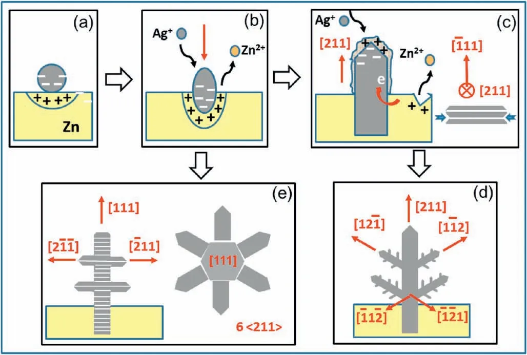
Fig.5.Schematic drawing of growth mechanism of Ag dendrites on a Zn plate.(a)Nucleation and growth of an Ag nanocrystal on a Zn plate.(b) Crystal growth of an Ag crystal at an early stage,which erodes Zn plate underneath.The red arrow shows the penetration direction of the Ag nanocrystal.(c) Growth of the trunk along the [211] direction with a fast growth speed.The hydrated cations deposit on the crystal surface to form an amorphous layer,followed by crystallization.The right side picture shows a cross section of the belt-like trunk.(d)Growth of secondary and tertiary branches.(e)A slow growth due to a low concentration of AgNO3,leading to growth of a trunk along the [111] direction,followed by growth of secondary branches along up to six <211>directions.
When a solution with a low concentration of Ag+is used to slow down the crystal growth,the process may be under thermodynamic control with the favored growth direction of a trunk along [111].Along this direction,the crystal has a six-fold symmetry and therefore,the shape of the trunk becomes hexagonal rods instead of a thin plate(Fig.5e).Up to six secondary branches can grow up along the six <211>axes,which are parallel to the (111) plane.The overall shape of the particles is King Mace-like.
3.2.Copper nanodendrites
In comparison with silver,copper is more economical,earthabundant and sufficiently conductive.Such properties make copper a good candidate for applications in electrode modification,microdevices and hydrophobic surfaces[36-38].Since the crystal structures of Cu and Ag are similar,we expected the growth of their dendritic particles during the replacement reactions to be similar as well.
3.2.1.Fern leaf-like copper dendrites
The replacement reaction between Al and Cu2+was very fast due to the large difference in reduction potentials of these two cations:Cu2+→Cu(+0.34 V)and Al3+→Al(-1.66 V).The reaction was carried out in the presence of HCl to prevent the formation of an Al2O3barrier on the Al surface.On the other hand,H+was in competition with Cu2+cations for reduction to form H2gas,significantly decelerating the reduction of copper.
Because the reaction was very fast,change of the reaction temperature from 4 to 35°C made no detectable difference to the products.Furthermore,fern leaf-like copper dendrites formed in all solutions with different CuSO4concentrations.Fig.6a and b shows typical copper dendrites produced on an Al plate in a solution with 50 mM of CuSO4and 100 mM of HCl at a reaction time of 1 h.It can be seen that the copper dendrites are composed of a primary trunk of 10-30 μm in length with secondary branches around 0.2-4 μm in length.In some particles,tertiary branches are not obvious (Fig.6a) and some have tertiary branches of 0.5-2 μm in length(Fig.6b).According to the XRD pattern in Fig.6c,the crystal structure of the produced Cu dendrites is fcc with the unit cell dimension a3.6151 Å,space group(ICSD 43493).It is noted that a few weak peaks in the XRD pattern are indexed to the cubic structure of Cu2O(a4.27 Å),which is probably an intermediate phase during the reduction of Cu2+to Cu.
The arrow in Fig.6a points to an end of a dendritic particle,at which no secondary branches developed in a length of about 1 μm.Similar to the Ag dendrites,this end can be called the‘root’of the dendrite,which is supposed to originally pin into the Al plate,ensuring the continuity of the replacement reaction.The geometric relation between the Cu dendrites and Al plate can be confirmed by SEM images of some early stage Cu particles as shown in Fig.S6 in the SI.
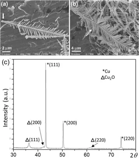
Fig.6.(a)and(b)SEM images of copper dendrites produced under the conditions of 50 mM of CuSO4,100 mM of HCl and reaction time of 1 h.(c)XRD pattern of the copper dendrites,showing the Cu crystal structure with a minor phase of Cu2O.
The prioritized crystal growth directions in the Cu dendrites were determined by SAED.The TEM image in Fig.7a shows some secondary branches growing out from a primary trunk.The shape of these branches is baseball bat-like with the diameter of the bottom part much smaller than the top part.Fig.7b shows the corresponding SAED pattern,indexed to the fcc unit cell of Cu.Consequently,the growth direction of the trunk isThe growth directions of the secondary branches on the two sides of the trunk are[211]andand the view direction is thereforeaxis.Through tilting the specimen,SEM images confirm the Cu dendrites are flat (Fig.S7,in the SI).Therefore,these Cu dendrites are similar to the fern leaf-like Ag dendrites as shown in Fig.2,exhibiting a kinetic bias favoring growth in the <112>directions.
On the other hand,since Cu has higher stacking fault energy(78 m J m-2) than Ag (16 m J m-2),Cu dendrites contain fewer defects and therefore,the intensity of the satellite diffraction spots,1/3{422},in the SAED pattern in Fig.7b is much weaker than those from the Ag particles(Fig.2)[39].These satellite diffraction peaks were not observed for most copper particles examined and the growth orientation of <211>would not appear to be influenced by these defects,as predicted by the TPRE mechanism.
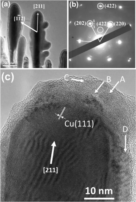
Fig.7.(a)TEM image showing secondary branches of a copper dendrite,and(b)the corresponding SAED pattern indexed to the fcc Cu structure.(c)HRTEM image of a tip of a secondary branch.Some Cu2O nanocrystallites developed in the disordered coating layer are indicated by the A-D arrows.
Another interesting phenomenon shown in the TEM image in Fig.7a is that the crystal is fully covered by an amorphous layer,~10 nm in thickness.Fig.7c is a HRTEM image of a tip of a secondary branch in a Cu dendritic particle.A surface coating layer of 5-15 nm in thickness is clearly visible.The light image contrast of this surface layer indicates that the mass density of the layer is much lower than the density of the core crystal.The principal d-spacing marked in the core crystal is 2.1 Å,which corresponds to the (111) planes of the fcc Cu structure.Interestingly,nucleation and growth of nanocrystals took place inside the coating layer.The d-spacings measured from the fringes of these nanocrystals(A to D)are about 2.5 Å,which cannot be indexed to the Cu metal structure,but can be indexed to the (111) atomic planes of Cu2O.This result is consistent with the result of XRD in Fig.6c.
Consequently,in a multi-step formation,the Cu2+cations in an aqueous solution exist as [Cu(H2O)6]2+,which are attracted by the negatively charged crystal surface to form an amorphous layer,followed by a reduction and crystallization to Cu2O nanocrystals.These nanocrystals would be further reduced by receiving more electrons and contribute to the growth of the core crystal or grow independently to form a new dendritic particle at the tip of the parent branch,as seen in Fig.S8,in the SI.Therefore,the controlling step of the crystal growth of the Cu dendrites is the reduction of Cu2O at the crystal/coating interface.
When a primary trunk grows along thedirection,two rows of secondary branches normally grow outwards along the[211]anddirections,not inwards along the opposite directions of the secondary branches,andas predicted by DLA theory.However,in some Cu dendrites,inwards growth of secondary and tertiary branches was often observed,as shown in Fig.S9,in the SI.
3.2.2.Fence-like copper dendrites
The fern leaf-like morphology of copper dendrites with the favored growth direction of <211>was produced in all the solutions with different concentrations of CuSO4(Fig.S10,in the SI).Another plausible way to alter the growth rate is to increase the acidic concentration,allowing the reduction reaction of H+to take more sites on the Al surface.When the CuSO4concentration was 50 mM and the HCl concentration was increased to 150 mM,a new morphology,fence-like,was observed,as shown in Fig.8a and b.The angle between the primary trunk(20-30 μm in length)and the secondary branches(1-3 μm in length) is 90°.
Fig.8d is an SAED pattern taken from the dendrite in Fig.8c,indicating that the growth direction of the primary trunk is determined aswith two rows of secondary branches along the[111]and opposite axes.A twin structure in the[111]direction is also observed.
4.Conclusions
This work demonstrates the use of microstructural information of Ag and Cu nanodendrites for better understanding their growth mechanisms in GRR.At an early stage,erosion of sacrificial plate and growth of Ag or Cu nanocrystals take place at the same sites,allowing the Ag or Cu crystals to insert into the sacrificial plate.The crystal growth relies on a strong Coulombic force between the negatively charged metal crystal surfaces and the Ag+or Cu2+cations in solutions,forming an amorphous coating layer on the metal surface.The cations undergo a reduction,followed by crystallization at the metal/coating interface.In the case of Cu,the reduction of Cu2+takes two steps with Cu2O as an intermediate phase.The crystal growth direction is usually along the <211>axes as is kinetically governed,leading to a fern leaf morphology of the particles.However,reducing the crystal growth rate can turn the growth direction to the thermodynamically controlled[111]axis.Different combinations of the [111] and <211>growth directions result in different shapes of the dendrites;e.g.King Mace-like Ag and fence-like Cu.The present work demonstrates that the crystal growth orientation and shape of the metal dendritic particles via GRR may not be merely governed by the DLA and TPRE mechanisms,but can be altered by other factors,such as interaction between the crystal and the precursor,speed of crystal growth,as well as the intrinsic properties of the materials.The information may be helpful in understanding the formation mechanisms of other metal and nonmetal dendritic particles.
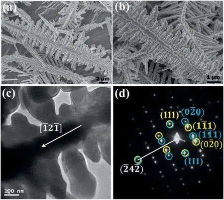
Fig.8.(a)and(b)SEM images of copper dendrites prepared in a solution with 50 mM of CuSO4 and 150 mM of HCl whose secondary branches are perpendicular to the primary trunk.(c)TEM image of such a dendrite.The arrow indicates the growth direction of the trunk.(d)The corresponding SAED pattern.The two sets of diffraction spots circled in yellow and in blue respectively have a mirror symmetry,indicating a twin defect (the white line can be regarded as the location of the twin plane).
Declaration of competing interest
The authors declare that they have no known competing financial interests or personal relationships that could have appeared to influence the work reported in this paper.
Acknowledgements
JLC thanks Chinese Scholarship Council and University of St Andrews for financial support.
Appendix A.Supplementary data
Supplementary data to this article can be found online at https://do i.org/10.1016/j.pnsc.2020.12.007.
 Progress in Natural Science:Materials International2021年1期
- Progress in Natural Science:Materials International的其它文章
- Dynamic response characteristic of 7N01/7A01/7050 aluminium multilayer plate at high strain rate
- Synergetic effect of multiple phases on hydrogen desorption kinetics and cycle durability in ball milled MgH2-PrF3-Al-Ni composite
- Highly mechanical and high-temperature properties of Cu-Cu joints using citrate-coated nanosized Ag paste in air
- Ab-initio investigation for the microscopic thermodynamics and kinetics of martensitic transformation
- Rapid directionally solidified microstructure characteristic and fracture behaviour of laser melting deposited Nb-Si-Ti alloy
- Microstructure evolution and mechanical properties of a hot-rolled Ti alloy
