
Electric transmission behavior of self-assembled Cu-W nano multilayers
2021-07-30 12:11:18MengzhaoYangTianleXieLicaiFuJiajunZhuWulinYangDeyiLiLingpingZhou
Mengzhao Yang,Tianle Xie,Licai Fu,Jiajun Zhu,Wulin Yang,Deyi Li,Lingping Zhou
College of Material Science and Engineering,Hunan University,Changsha,Hunan Province,410082,China
Keywords:Self-assembling Cu-W nano Multilayer Resistivity Interface F-S model
ABSTRACT Metallic nano multilayers were usually prepared by dual targets alternating deposition method.In this paper,a series of self-assembled Cu-W nano multilayers with different modulation periods were deposited on single crystal silicon substrate by dual targets confocal magnetron sputtering technique.The self-assembled film presented an alternation of W-rich layer and Cu-rich layer.The degree of coherence of the layered interface can be adjusted by controlling both the solid solubility of W-rich and Cu-rich layers.The film resistance increment of the self-assembled Cu-W multilayers is only 14% when the modulation period decreases from 68.2 nm to 5.3 nm,having less size effect compared to the film prepared by alternating deposition method.It noticed that the film resistance even decreased slightly when the modulation period decreased to below 5.3 nm.These results suggested that the coherence could weak the interface scattering ability to electrons,so the self-assembled Cu-W multilayers have lower resistance than the multilayer prepared by alternating deposition technique.This study presented a new pathway to enhance the conductivity of the multilayers.
1.Introduction
Metallic nano multilayers exhibit different properties from bulk materials due to their nanometer scale and abundant interfaces [1,2].Owing to the layered structure character,the total resistivity of a multilayer film is usually caused by four factors[3]:phonon scattering,impurity scattering,interface scattering and grain boundary scattering.According to the Matthiessen’s rule,the total resistivity can be expressed as,ρfilm=Δρphonon+Δρimpurity+Δρinterface+Δρgrainboundary[4].The phonon scattering and impurity scattering can be seen as the background scattering which is included in bulk resistivity of metals (ρ0=Δρphonon+Δρimpurity)[3,5].It is recognized that the electrical property have significant size effect,which can be tuned by the nature of interfaces.So the interface and grain boundary scattering are usually regarded as the main factors for the resistivity of multilayers.The F-S model[6,7]largely interprets the effect of interface scattering or surface scattering on the resistivity of the film.Dimmich developed a new model by taking interface scattering into account based on theM-S model[8,9],which considered the effect of grain boundaries scattering on resistivity Based on theabove-mentionedtheories,many researches have successfully explainedthe resistivitysize effect of resistivity of metals and alloys films [3,10-12].
The disordered interface arranges irregularly,it will scatter the free electrons and increase the resistivity.While a reduction in the modulation period(λ)will increase the density of the interface in the film.So,when the modulation period was comparable to electron mean free path(EMFP),the interface scattering increaseddramaticallythat resulted in the increase of the resistivity [3].Interface scattering enhances the resistivity of the nano multilayers,while coherent interface hasthelowest enhancement effect among these interfaces.So,it is necessary to obtain coherent interfaces in order to reduce the size effect of nano multilayer.Usually,nano metallic multilayer films have been prepared by alternating deposition method (deposit only one metal at a time and periodically change the type of deposited metal) 3,5,12,13.Sincethecoherent interface only can be formed when the surface energy mismatch of the components in the system is small and the atomic radius satisfies a certain relationship.So onlyina few systems,such as Cu-Ni,Cu-Co and Cu-Ag,the coherent interface can be formedduring alternating deposition [13-16].For most systems,the interfaces of the multilayer film are incoherent,such as Cu/W,Cu/Cr,Cu/V.For forming coherent interface,the composition of sub-layer can be designed as solid solution instead of pure metal to reducethelattice mismatch ofthesub-layers.Based on this deduction,we proposed the self-assembling technique to meet the requirements of solid solution.The self-assembled Cu-Wmultilayers havebeen prepared successfully by dual targets confocal magnetron sputtering technique [17].And the interfaces ofthe multilayers prepared by co-deposition methodare in a coherent or semi-coherent state,which is different from the film obtained by alternating deposition [2].Cu-W nano-multilayer film has been widely applied in the field of microelectronics due to its special electrical properties and low expansion coefficient,so its electrical properties deserve detailed study.Here,a series of self-assembled Cu-W nano-multilayered films with differentλwere prepared bydual-targetconfocal magnetron sputtering technique.And the effect of the interfaces on the resistivity of self-assembledmultilayerswas investigated.
2.Experimental details
Self-assembled Cu-W multilayers were deposited on single crystal silicon (100) substrate by dual targets confocal magnetron sputtering technique (MIS800).The targets were arranged in a confocal method,and the angle between the target center and the substrate center was 30°.The purity of the Cu target and the W target is 99.99%and 99.95%,respectively.Both of their diameters are 50 mm.The siliconsubstrates wereput into acetone and alcohol for ultrasonic cleaning in turn and cleaned by Ar+ion beamwith an energy of 600 eV for 15 min before deposition.The base pressure in the vacuum chamber was less than 5×10⁻⁴Pa.Then argon with a flow rate of 60 sccm and a purity of 99.99%was used to keep the pressure inside the chamber at 1.0 Pa during sputtering.The temperature of thesubstrates were kept around at 20±2°Cby the cooling water system.The over-all composition of films was about 60 at.%W,which was controlled by the power of two targets.The sample stage rotated continuously during the deposition process,and theλcan be adjusted by the stage rotation speed (RPM).The deposition time was 40 min which made the thickness of the films about 2 μm.
The resistivity of multilayers usually varies with their modulation periodλand the nature of the interfaces between the layers [3,5].The modulation periodλoftheself-assembled multilayer films can be controlled by therotation rateof the sample stage.So,in this paper,the corresponding rotation speeds of the 1 RPM,2.5 RPM,5 RPM,10 RPM,20 RPM,respectively,have been designed.
The phase analysis can be achieved by XRD (X-ray diffractometer,Miniflex 600) (Cu-Kαradiation,λ=0.154056 nm).Cross-sectionalmorphologies and the thickness of films were obtained by FESEM(field emission scanning electron microscope,Hitachi S-4800).The elements distribution of films was measured by FEI Quanta 200 SEM with EDS(energy-dispersive spectrometer).TEM (transmission electron microscope,FEI Titan G260-300) was used toanalyzethenano-structure and crystallographic.
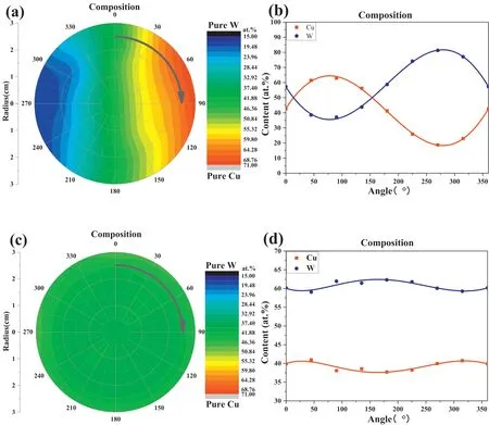
Fig.1.The deposition field(a)the sample stage does not rotate and(c)the sample stage rotates at a speed of 2.5 RPM;The composition fluctuation at a radius of 22 mm of the film (b) the sample stage does not rotate and (d) the sample stage rotate at a speed of 2.5 RPM.
The sheet resistance was measured by a standard four-probe tester(RTS-8)at room temperature.The resistivity of the Si substrates is 8.6×10⁶μΩ cm,which is 4 orders of magnitude higher than film resistivity(about 102μΩ cm).Therefore,the influence of the substrates on the resistivity of films can be ignored.To avoid the edge effect,8 points were selected from the films at the symmetrical position with a radius of 22 mm,and each area was measured at least four times at different locations.
3.Results and discussion
3.1.Assembled Cu-W nano multilayer
The deposition field (Fig.1a) under this experimental conditions,wasachieved by determining the composition distribution C(Φ,r)of the Cu-W film with a diameter of 76.2 mm when the sample stage does not rotate (0 RPM).For this purpose,25 positions in a polar coordinate system were selected for EDS measurement:Φ was varied with steps of 45°,each Φ four positions r=0 mm,r=15 mm,r=22 mm and r=28 mm were measured.In the deposition field,red and blue represent Cu and W respectively.It is obvious that approximate symmetrical Cu-rich and W-rich regions are formedon both sides ofthe center line.In particular,the contents of Cu and W deposited on the substrate at a radius of 22 mm will change along with the wavy curve(Fig.1b).It can be expected that when the sample stage rotates,the substrate will appear alternately in the regions of Cu-rich and W-rich.The multilayer film with alternating Cu-rich layers and W-rich layers will be formed on the substrate.Like the alternating deposition,increasing the rotation speed will reduce the modulation period of themultilayers,but there isno duration for samples direct exposure below the targets.Adjusting the power of the Cu and W target can control the composition and deposition rate of the Cu-rich and W-rich regions in the deposition field,so that the modulation ratio (η) and over-all composition of the multilayer film can be controlled.It can be expected that the Cu-rich and Wrich areas will disappear as the rotation speed increases(Fig.1c and d).Muller et al.[18] also observed similar deposition field of Cu-Ta films prepared by co-sputtering deposition,and obtained nano multilayers.However,this process condition mentioned above is notasufficient condition for forming a self-assembled multilayer film [17],and the intrinsic factor of elements plays a crucial role in it.
Fig.2 shows the XRD patterns of the self-assembled Cu-W multilayers with different modulation period.The diffraction peaks of the multilayers shift to a higher angle relative to the pure W,which shows the formation of W-based solid solution[19].Because the atomic radius of W (aw=0.137 nm) is larger than Cu (aCu=0.128 nm),the crystal plane spacing will become smaller with respect to pure W after solid solution of Cu atoms in the W matrix,and the diffraction peaks will shift to higher angle according to the Bragg equation.Note that the shape of the diffraction peaks are not symmetrical,indicating that the composition changes continuously in sub-layer [17].
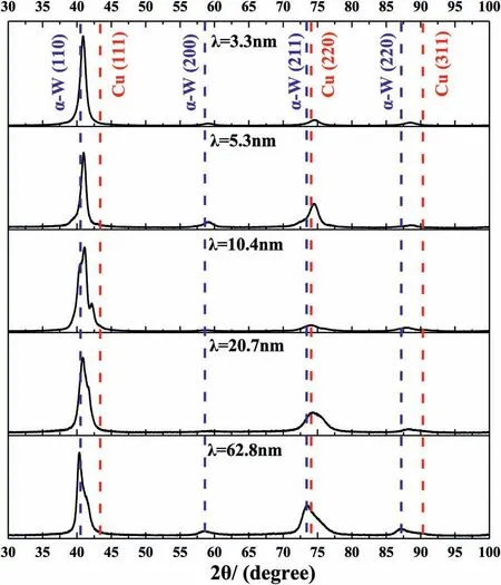
Fig.2.XRD patterns of self-assembled Cu-W multilayer films with different modulation period.
All the cross-sectional images of the films with different rotationrateexhibit distinct columnar and dense structures(Fig.3).There no obvious pores can be detected.Thelaminatedstructure can be observed by transmission electron microscope.
STEM and mapping images of the film (Fig.4a and d) show a modulation period of 20.7 nm.It is obvious that the thickness of the W-rich layer is thicker than Cu-rich layer,but the SAED presents fcc structure but not bcc structure.The over-all composition of the film is about 60 at.%W which is measured by EDS.These results obviouslypresentthat the Cu-W film prepared by co-sputtering technique has a multilayer structure.The composition fluctuation curve obtained by line scanning indicates the composition of the self-assembled Cu-W multilayer continuously change along the thickness direction.Therefore,there is a small mismatch between the metal atoms on both sides of the interfaces,which is favorable for forming coherent or semi-coherent interfaces.Usually,in contrast,the films obtained by alternating deposition method are composed of pure metal sub-layers[3,5,12,13].Owing to the similar composition near the layer interface,thesemi-coherentand coherent interface forms (Fig.4c).It is expected that this interface has a much smaller scattering ability for electrons than the films obtained by alternating deposition.
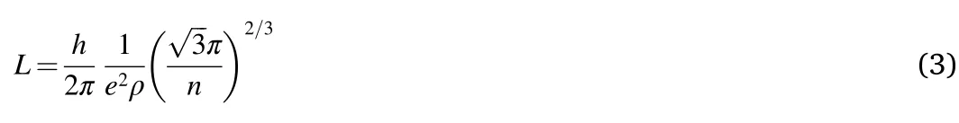
As the rotation speed of sample stage increases,the modulation period λ of the Cu-W multilayersdecreases gradually.Theλdecreases to be about 3.3 nm when the rotation speed increases to 20 RPM(Fig.5).The Cu content fluctuation decreases from 20.5-64.0 at.%to 26.7-42.7 at.%(Figs.4d and 5d)with decreasing of the modulation periodλ.This corresponds to the increasingly symmetrical diffraction peak shape of the XRD pattern.It’s noted that the Cu-rich layer in this film is only relatively enriched,in fact,both the W content are larger than that of Cu content.Because the composition difference adjacent layers is small,the lattice distortion after forming the interface is also small,which is favorable for forming a coherent interface.When theλdecreases to 3.3 nm,the interfaces between layers become fully coherent(Fig.5b and c).
3.2.The resistivity of Cu-W nano multilayer
The curve in Fig.6 shows the resistivity of Cu-W single layer film(0 RPM) variation with W content.The resistivity increases first and then remains essentially unchanged as the Wcontent increases.Within the composition range (34.6 at.% W~81.3 at.% W),the resistivity of the Cu-W film ranges from 96 μΩ cm to 154 μΩ cm,which is much larger than the resistivity of bulk W(ρW=5.28 μΩ cm)and Cu(ρCu=1.68 μΩ cm) at room temperature [20].Vüllers also indicated that resistivity of Cu-W film ranges from 94 μΩ cm to 159 μΩ cm when the content of W increases from 22 at.%to 87 at.%[21].According to previous reports,the high resistivity is mainly caused by thestrengtheningelectron scattering at the interfaces of the columnar structures due to the presence of pores [5,22].
The resistivity of Cu-W multilayer increases rapidly as the modulation periodλdecreases from 20 nm to 5.3 nm (Fig.7).This trend is similar to the change in resistivity of films obtained by alternating deposition method[1,5,13].This phenomenon is caused by an increase in interface density in the film,which results in enhancing interface scattering.When theλcontinuous decreases to below 5.3 nm,the resistivity no longer increases even decreases,which is different from the above-mentioned studies and the simulated result from the F-S model.In the previous microstructure analysis,it was mentioned that as the modulation period decreases,the atoms at the interface will become more coherent.Therefore,the interface scattering is weakened,which makes it possible to reduce the resistivity of films.
The resistivity of the films is usually higher than that of the bulk materials and increases significantly as the thickness decreases[23,24].It can be largely interpreted by the Fuchs size effect [7].When the thickness of the film is lower than the EMFP,the surface will constrain the electrons transmission,thereby increasing the film resistivity.Conversely,if the film thickness is larger than the EMFP,the resistivity ofthefilm is not sensitive to the thickness.The corresponding theory is the F-S model and the equation is given by Refs.[6,7]:
where ρFSis the resistivity of film and ρ0is the resistivity of bulk material;κ(=t/L) is the ratio of film thickness (t) to EMFP (L) of bulk material;pis the surface specularity coefficient,which varies from 0 to 1,wherep=0 for totally diffuse andp=1 for perfect specular reflection.When the film thickness is greater than the EMFP,this equation can be simplified 25:
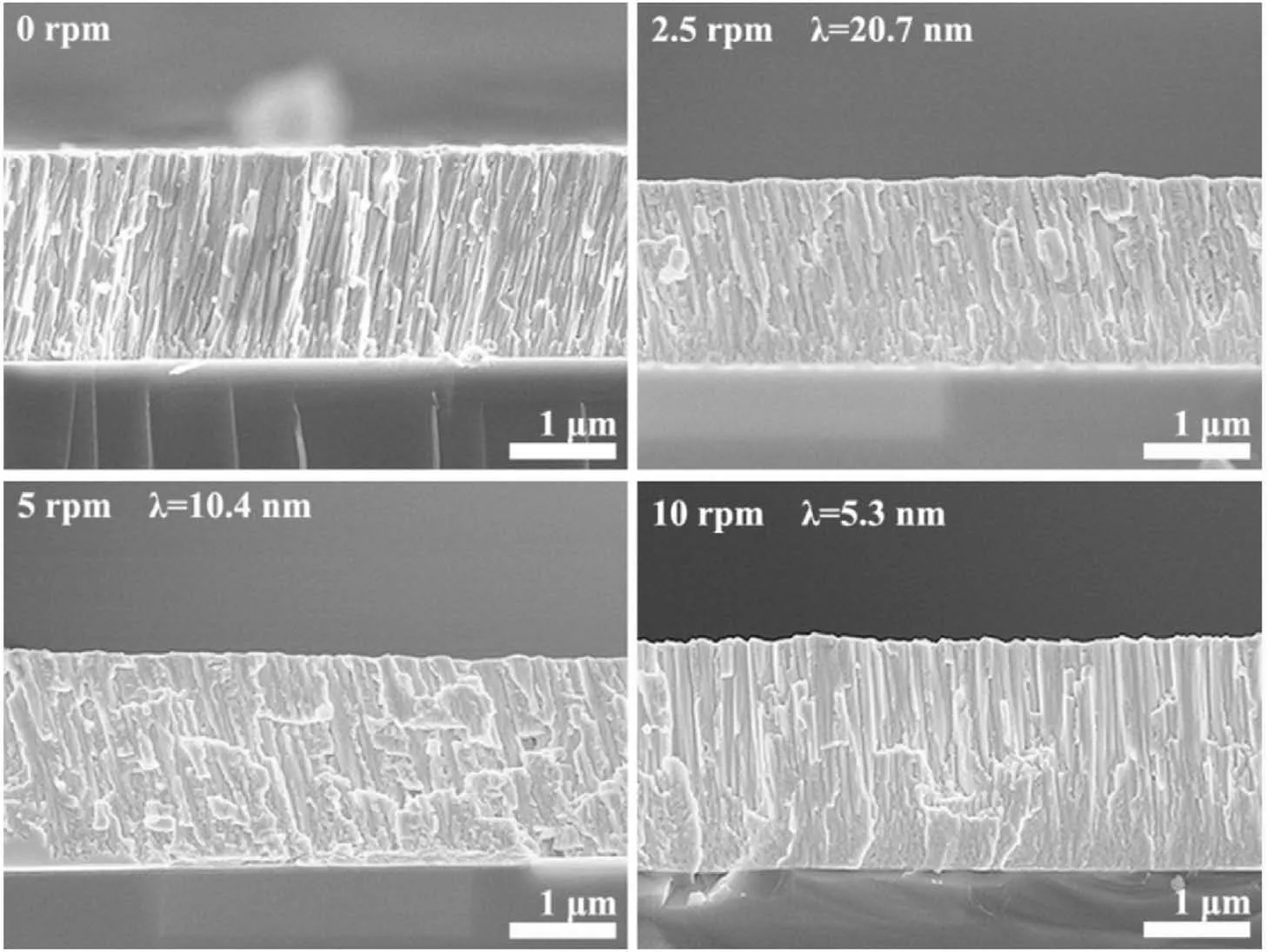
Fig.3.The cross-sectional SEM morphologies of films with different modulation periods.
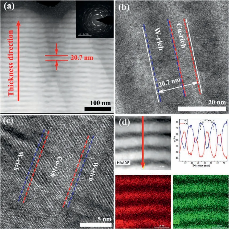
Fig.4.Cross-sectional of self-assembled Cu-W film with a modulation period of 20.7 nm (2.5 RPM):(a) STEM image;(b),(c) HRTEM image;(d) EDS analysis.
The EMFP of bulk Cu and W is 39 nm and 19.1 nm at room temperature [11],respectively.The thickness of the films prepared in this case is about 2 μm,which is much larger than the EMFP of the bulk Cu and W.Therefore,the Fuchs size effect can be neglected according to Eq.(2).So the resistivity of these 0 RPM films can be regarded as the resistivity of the corresponding component bulk metal[5].
According to the fluctuation of the composition of the multilayer films(Figs.4d and 5d)and the resistivity of the 0 RPM films(Fig.6),the resistivity of Cu-W multilayers varies with the distance during one period (Fig.8).The continuous variation of the resistivity at the interfaces which is different from the sudden change in films obtained by alternating deposition method.This continuous variation makes it difficult to derive an accurate value of the resistivity for Cu-rich layer,W-rich layer and individual layer.The resistivity of the self-assembled multilayer film should be obtained by other means.
The EMFP of metals can be calculated by Ref.[5]:
whereeis the electron charge;his the Planck’s constant;nandρare carrier concentration and resistivity of the metal,respectively.
The carrier concentrations of bulk Cu[12]and W are 8.5×1028and 4.5×1028m-3,respectively.The carrier concentration of bulk W is obtained by substituting its resistivity and EMFP into Eq.(3)(ρW=5.28 μΩ cm,LW=19.1 nm).Here,the carrier concentration of the films can be approximately calculated by,n=0.4 nCu+0.6 nW=6.1×1028.Therefore,the EMFP of the film must be smaller than the EMFP of bulk W due to the increased resistivity and carrier concentration.By considering lack of the bulk resistivity,the resistivity of the film with a modulation period of 68.2 nm (119 μΩ cm) is assumed to the bulk resistivity of individual layer (ρ0),since 68.2 nm is much larger than the EMFP and the Fuchs size effect is negligible.Then the EMFP of Cu-W multilayer can calculate to be 0.69 nm by calculating Eq.(3).
If the grain size is comparable to the EMFP of the metal,the grain boundaries will restrict the electronictransmission.By introducing the grain boundary scattering coefficient(R)[8],theM-S model explains successfully the grain boundary scattering effect on the resistivity of the film.The grain size can be estimated by the Scherrer’s equation based on XRD patterns of Cu-W multilayers.The result shows that the grain sizes of all the multilayers with different modulation periods are larger than 60 nm and much larger than the calculated EMFP.In addition,the grain boundary scattering was strongly enhanced by the pores,thus it is difficult to extract the role of the grain boundary itself.For the reasons mentioned above,it can be considered thatthegrain boundary scattering is included in background scattering.Therefore,phonon scattering,impurity scattering and interface scattering are all included in ρ0(ρ0=Δρphonon+Δρimpurity+Δρinterface).Therefore,this study only needs to consider the interface scattering based on the F-S model.
Fig.5.Cross-sectional microstructure of self-assembled Cu-W film with a modulation period of 3.3 nm (20 RPM):(a) STEM image;(b),(c) HRTEM image;(d)EDS analysis.
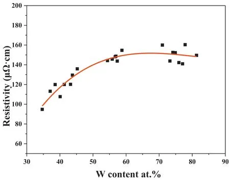
Fig.6.Resistivity of Cu-W films with a rotation speed of 0 RPM as a function of W content.
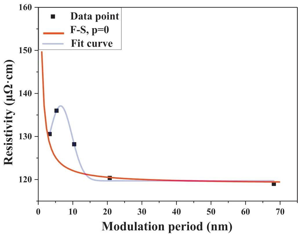
Fig.7.The resistivity of self-assembled Cu-W multilayer films as a function of modulation period;Comparison of the measured values of resistivity of selfassembled Cu-W multilayer films and simulations based on F-S model.
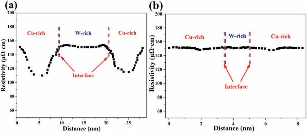
Fig.8.(a)Resistivity fluctuations of self-assembled Cu-W multilayer film with a modulation period of 20.7 nm.(b)Resistivity fluctuations of self-assembled Cu-W multilayer film with a modulation period of 3.3 nm.
Generally,the resistivity of the metal multilayer films increases with the increase of the residual stress [26,27].And the residual stress of multilayer films can be tuned by the several parameters,such as the sputtering pressure,the deposition temperature,and thickness of films and individual layers [28-30].For this work,all of the parameters are constant (film thickness,sputtering pressure,deposition temperature,substrate and target power),except for the modulation period.the composition of the self-assembled Cu-W nano-multilayer films obtained by co-deposition transitions smoothly along the growth direction,and the lattice parameters gradually change [17],which may cause continuously changing internal stress,and it is expected that there will be no significant stress contribution at the interfaces.As mentioned earlier in this paper,the decrease of the modulation period of the self-assembled Cu-W nano-multilayer films will lead to smaller amplitude of composition fluctuation and more coherent interfaces,so it is expected that the residual stress in the film will change to a certain extent.Micro-stress and grain refinement will jointly lead to the broadening of the diffraction peaks of materials.Based on the XRD patterns,the Hall method was used to calculate the micro-strains of the self-assembled Cu-W multilayer films with different modulation periods,i.e.taking sinθ as the abscissa and FW(s)×cosθ as the ordinate,and fitting with the least square method.The calculated results show that the micro-strain is distributed in the range of 1.0%-1.6%,and there is a slight decrease trend with the decrease of modulation period,which is consistent with the increasingly coherent interfaces.The effect of the change of micro-strain in this range on the resistivity of self-assembled Cu-W multilayer films needs further study.
According to the F-S model,the resistivity of an individual layer can be calculated according to Eq.(3).Thus the resistivity of multilayer films can be calculated from ρFSwith the law of resistance in parallel[3].The simulation result is shown in Fig.7.Surprisingly,even with p equal to 0,the simulated curve is still below the measured data.This is obviously not true,because the self-assembled Cu-W multilayerfilmshave coherent or semi-coherent interfaces which result in a smaller scattering ability for electrons,i.e.,a largerpvalue.Theseresults may be caused by the untight structure of the multilayers,especially for the small period structure,which enhances the background resistivity.In addition,there must be fluctuation of EMFP in a modulation period because of the resistivity and composition fluctuations (Fig.8),this study takes the average value of EMFP in a modulation period.Misra’s work 5 got a similar result which uses the same method to obtain the EMFP,but Misra attributed the reasonforthe decreasing of intrinsic resistivity of the Cu layer as the modulation period decreases.
Manyresearchersreported that the resistivity of multilayers increases with the modulation period.For example,Carcia et al.[10]show that when the modulation period is reduced from 100 nm to 20 nm,the resistivity of the Pd-Au multilayer film increases from 15 μΩ cm to 40 μΩ cm.Lima’s work [12] indicates that the resistivity of Cu-Nb multilayer film will increase from 2.5 μΩ cm to 25 μΩ cm as the modulation period reduced from 80 nm to 5.9 nm.Fig.7 presents that the maximum resistivity of self-assembled multilayer is only increased by 14% (from 119 μΩ cm to 136 μΩ cm),having less size effect caused by the decreases of modulation periodλ.Previous study has shown that larger p will result in less size effect[31],Thus,the self-assembled Cu-W multilayers with coherent interfaces have a weak interface scattering effect when theλdecreases to below 5.3 nm.Wei et al.[13] also indicated that resistivity of Cu-Ag multilayers with coherent interfaces still maintained a certain range even if the modulation period was less than the EMFP.
4.Conclusion
Self-assembled Cu-W nano multilayers with different modulation periods are prepared by arranging the targets in a confocal method and keeping the sample platform rotation during deposition.The multilayersconsistof alternating Cu-rich and W-rich layers.By adjusting the deposition parameters,optimizing the degree of solid solution,the coherent interface forms gradually with the modulation period decreases to below 5.3 nm.The simulation resistivity based on the F-S model does not match the measured data very well.Owing to forming of the coherent interface,the self-assembled Cu-W multilayers have less size effect compared to the multilayers obtained by the alternating deposition method.
Declaration of competing interest
The authors declare that they have no known competing financial interests or personal relationships that could have appeared to influence the work reported in this paper.
Acknowledgements
This work was supported by the National Natural Science Foundation of China (51675169).
Appendix A.Supplementary data
Supplementary data to this article can be found online at https://doi.org/10.1016/j.pnsc.2020.11.001.
 Progress in Natural Science:Materials International2021年1期
- Progress in Natural Science:Materials International的其它文章
- Dynamic response characteristic of 7N01/7A01/7050 aluminium multilayer plate at high strain rate
- Synergetic effect of multiple phases on hydrogen desorption kinetics and cycle durability in ball milled MgH2-PrF3-Al-Ni composite
- Growth mechanisms of Ag and Cu nanodendrites via Galvanic replacement reactions
- Highly mechanical and high-temperature properties of Cu-Cu joints using citrate-coated nanosized Ag paste in air
- Ab-initio investigation for the microscopic thermodynamics and kinetics of martensitic transformation
- Rapid directionally solidified microstructure characteristic and fracture behaviour of laser melting deposited Nb-Si-Ti alloy