金刚石纳米线氮空位色心的表面与尺寸效应
2021-07-11 16:19刘小峰李震宇杨金龙
高等学校化学学报 2021年7期
胡 伟,刘小峰,李震宇,杨金龙
(合肥微尺度物质科学国家研究中心,中国科学技术大学,合肥230026)
Nitrogen-vacancy(NV)centers in diamond[1―3]have been widely studied experimentally and theoretically due to their outstanding properties and wide-ranging applications in condensed matter physics fields including reliable radiations detector[4],spin readout techniques[5],biology[6,7],Rabi Oscillation[8],single photon source[9],one-and two-qubit operation[10―12],magnetometry[13,14],magnetic sensing[15],and other quantum application[16,17].An NV center is composed of a vacancy with one adjacent carbon atom replaced by a nitrogen atom[18―21].Two types of charge states,namely,neutral NV0and negative NV-centers,have been observed experimentally,which can be discriminated by their photoluminescence spectrum and interconvert into each other by laser excitation[22,23].In detail,the NV0center has an unpaired electron and is paramagnetic,while the NV-center has anS=1 ground state.In particular,the NV-state dominates in the high-purity diamond.Therefore,such two different charge states process two different magnetic properties,and it is desirable to control the charge states of NV centers in diamond for their practical applications in experiments.
Interestingly,a number of experimental studies have shown that photoluminescence properties of the NV centers are affected by the sizes[24―26]and surfaces[27―32]of diamond.To understand these experimental observations,our previous theoretical works have proved that surface functionalization can induce a nondecaying long range effectviasurface dipole layer localized on the diamond surfaces to control the relative stability of NV centers doped in diamond films[33]and nanodiamonds[34].In diamond films and nanodiamonds,NV-center prefers the oxygen saturated diamond and n-type fluorinated diamond,respectively,while the NV0is preferred for the p-type hydrogenated diamond[33,34].Furthermore,spin polarized defect states are not affected by the particle sizes and surface modifications in nanodiamonds and the[NV-]/[NV0]ratio slightly increases with the diameter sizes of the nanodiamonds[30,34].
Compared with diamond films and nanodiamonds,diamond nanowires(DNs),with energetically and mechanically viable structures[35],process a combination of wide-ranging properties,such as negative electron affinity,chemical inertness,high Young’s modulus,and the highest hardness[36―39].The creation of one-dimensional DNs with giant surface-to-volume ratio enhancements makes it possible to control and enhance the wideranging properties and promising applications of diamond[40].In particular,it has been proved that NV centers in DNs can produce ten times greater flux using ten times less power in experiments,with promising applications in photonics and quantum information processing[41].A robust single-photon source,namely,DNs doped with NV centers,can be fabricatedviatop-down nanofabrication techniques to realize isolated individual NV center[42].A single NV center with surface plasmon mode propagating along a chemically grown silver nanowire has also been observed in experiment[43],which can control the coupling of this particular emitter to the nanowires and directly compare the photon emission properties.It is a major advantage of DNs platform for this nascent material system and these important researches dig out a novel class of diamond-based quantum devices for quantum information processing,superior to conventional diamond films[33]and nanodiamonds[24,31,34].Therefore,how to control the electronic structures and stability of NV centers doped in DNs is crucial and desirable for their promising applications in photonics and quantum information processing.
Herein,we systematically investigate the electronic properties and stability of the NV centers doped in DNs by using large-scale spin-polarized first-principles density functional theory(DFT)calculations up to hundreds of atoms,and find that intrinsic properties of the two types of NV centers are independent of surface modification and diameter sizes of DNs.However,the two factors affect the formation energies of NV centers doped in DNs.Furthermore,such surface modification shows a nondecaying long-range effect on the stability of charged NV center doped in DNs induced by cylindrical surface electric dipole layer.In particular,DNs with n-type fluorinated diamond surfaces are more conducive to form the negative NV-center compared with p-type hydrogenated surfaces,which relatively favor the neutral NV0counterpart.
1 Theoretical Models and Computational Methods
DNs with energetically and mechanically viable structures as novel diamond-based nanomaterials[35],have attracted intense attention[36―39].The atomic and electronic structures of DNs strongly depend on the surfaces and sizes.There are three important kinds of DNs morphologies,dodecahedral,cubic and cylindrical.The dodecahedral DNs are bounded by diamond(110)surfaces in all lateral directions,with a square cross section,and have a principal axis in the[100]direction.The cubic DNs are bounded by two diamond(100)surfaces and two diamond(110)surfaces in the lateral directions,with a rectangular cross section,and have a principal axis in the[110]direction.The cylindrical DNs are bounded by two diamond(100)surfaces and two diamond(110)surfaces in the lateral directions,with a circular cross section,and have a principal axis in the[100]direction.Because the NV-center is polarized in the diamond(111)plane of[100]DNs in experiments[33],cylindrical DNs are adopted in this study.We theoretically design several types of DNs with different surface modifications and diameter sizes,and consider the clean[26―28],p-type hydrogenated[27,29,31]and n-type fluorinated[31]surfaces of cylindrical DNs to study the electronic structures and stability of nitrogenvacancy(NV)centers in this work.
For cylindrical DNs,the width of the diamond(110)surfaces is set to M and the diamond(100)surfaces to N,thus,clean,hydrogenated and fluorinated DNs are denoted as CM_N_C,CM_N_H and CM_N_F,respectively.An example of cylindrical C3_3 DNs is shown in Fig.1.Initial atomic structures of DNs are cleaved from bulk diamond with dangling bonds on the surfaces.After structural optimization and surface reconstruction,stable clean C3_3_C DNs containing carbon atoms(C76)are obtained[Fig.1(A)].C3_3_C DNs can be passivated with hydrogen or fluorine atoms to obtain hydrogenated C3_3_H(C76H24)[Fig.1(B)]or fluorinated C3_3_F(C76F24)[Fig.1(C)]DNs.NV centers are doped in DNs with different lateral diameters(fixed the principal axis length of 1.07 nm in a 1×1×3 supercell)from 0.69 nm to 2.18 nm,including C2_1_X(C63X36),C4_1_X(C135X60),C6_1_X(C231X84),C3_3_X(C228X72),C4_3_X(C291X84),C2_5_X(C327X84),C4_5_X(C495X108),C6_3_X(C435X108)and C6_5_X(C687X132),where X represents the clean(C),hydrogenated(H)and fluorinated(F)surfaces.It is worth noting that the NV centers are regarded as the center of DNs in order to facilitate the calculations and comparisons.

Fig.1 Top and side views of atomic structures of clean C3_3_C(A),hydrogenated C3_3_H(B),fluorinated C3_3_F cylindrical DNs(C),and the corresponding electronic band structures(D—F)
Large-scale spin-polarized first-principles DFT calculations are performed in the SIESTA(Spanish Initiative for Electronic Simulations with Thousands of Atoms)package[44].The local spin density approximation(LSDA)[45]is chosen because of its good description of electronic and magnetic properties of NV centers in diamond[46―48].Further test calculations under the generalized gradient approximation of Perdew,Burke,and Ernzerhof(GGA-PBE)[49]also give similar results[46].All the elements use a doublezetaplus polarization orbital basis(DZP)to describe the valence electrons within the framework of a linear combination of numerical atomic orbitals(LCAO)[50].The Brillouin zone is sampled with a 1×1×4 regular mesh for the electronic band structures of DNs in the unitcell.All the atomic coordinates are relaxed using the conjugate gradient(CG)[51]algorithm until the convergence criteria of energy and forces are less than 10-4eV and 0.2 eV/nm,respectively.
In order to evaluate the stability of NV centers doped in diamond,the formation energy(Eform)is evaluated as[52―55]

whereEpureandEdopedrepresent the total energy before and after the doping of an NV center with a charge stateqin diamond.μCandμNrepresent the chemical potential of carbon and nitrogen,which are determined by bulk diamond and nitrogen molecule,respectively.μerepresents the electron chemical potential of diamond hosting NV centers,which depends on the chemical environment in experiments[54].Generally,additional electron of the NV-center is easily derived from N-doped diamond[26],therefore,μeis aligned with the Fermi level of N-doped diamond in this work[54].We use a homogeneous positive background charge to compensate for the negative charge of NV-in diamond[56,57].It should be noted that the charge correction is ignored in this work,because we adopt a very large 4×4×4 supercell(a=b=c=1.07 nm andα=β=γ=90.0°)for bulk diamond with 512 carbon atoms,and a very large and the same supercell(a=b=4.0 nm,c=1.07 nm andα=β=γ=90.0°)for all the DNs doping the NV-centers to reduce the long-range Coulomb interactions(1/r)between the periodic images of the localized charges.
2 Results and Discussion
We first check the atomic structures and electronic properties of DNs[36―39]based on the C3_3 DNs with three different surface modifications(clean,hydrogenated and fluorinated)as an example(Fig.1).C3_3_C has a reconstructed structure,which introduces occupiedπand unoccupiedπ*states into fundamental band gap of diamond,resulting in isolated C=C dimmers on the diamond(100)surfaces and Pandey-chain structures on the(110)surfaces[58],with a narrow band gap(0.1 eV).Surface hydrogen and fluorine atoms remove theseπandπ*states,which makes C3_3_H and C3_3_F semiconducting wide band gaps of 4.5 eV and 4.8 eV,respectively.
The electronic structures of NV centers doped in DNs affected by surface modifications and diameter sizes are also studied.Total density of states(DOS)and spin-density isosurfaces are shown in Fig.2 and Fig.3.To check the effect of surface modification,C3_3_H and C3_3_F doped with NV centers are adopted.They are spin polarized with magnetic moments of 1.00 and 2.00μB for NV0and NV-,respectively.These spinpolarized defect states are totally located in the NV centers,in a good agreement with the previous theoretical studies on NV centers doped in bulk diamond[33,34,46].Thus,intrinsic properties of NV centers doped in DNs are independent of semiconducting surface modification,similar to the diamond films[33]and nanodiamonds cases[24,31,34].However,C3_3_C with NV centers is metallic due to the overlap between the NV defect states and surface C=Csp2states,showing small magnetic moments of 0.03 and 0.54μBfor NV0and NV-,respectively.In this case,two types of NV centers in diamond are weak spin-polarized and the spin-polarized states are mainly dispersed on the surfaces,which may be associated with the unknown non-fluorescent states observed experimentally in nanodiamonds[26,29].Therefore,C=Csp2states on the surfaces in clean C3_3_C DNs are not conducive to preserving magnetic properties of the NV centers in diamond,we mainly focus on the hydrogenated and fluorinated DNs in the work.
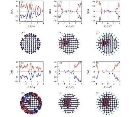
Fig.2 Total density of states(DOS)(A—F)and spin-density isosurfaces(A′—F′)for NV centers doped in DNs with three different surface modifications
To study the effect of diameter sizes,C4_3_X,C4_5_X and C6_5_X(X=H and F)are considered as shown in Fig.3.The largest system is C6_5_X that contains 819 atoms(687 carbon atoms and 132 hydrogen or fluorine atoms)computed by spin-polarized DFT calculations.We find that when doping with NV centers,these systems are spin-polarized with magnetic moments of 1.00 and 2.00μBfor NV0and NV-,respectively.Therefore,intrinsic properties of the NV centers doped in hydrogenated and fluorinated DNs are not affected by their diameter sizes,similar to nanodiamonds[24,31,34].

Fig.3 Total density of states(DOS)for NV centers doped hydrogenated and fluorinated DNs with different diameters
Interestingly,the formation energyEformof the NV-center doped in DNs can be increased for p-type hydrogenated C3_3_H(7.92 eV)but decreased for n-type fluorinated C3_3_F(5.31 eV),compared with the NV-center doped in bulk diamond(5.86 eV).However,this effect almost does not exist for NV0center doped in hydrogenated C3_3_H(7.31 eV)and fluorinated C3_3_F(7.39 eV)with corresponding NV0centers doped in bulk diamond(7.58 eV).These results are well consistent with previous experimental[29,30]and theoretical[33,34]studies for the NV centers doped in diamond films and nanodiamonds.
Using hydrogenated and fluorinated DNs as examples,surface and size effects on the stability of NV centers are studied.Fig.4(A)plots the formation energy of two types of NV centers doped in DNs with different surface modifications and diameter sizes.When the DNs diameters are small,surface modification can significantly change the stability of NV centers,and they are more stable in small DNs,which is different to NV centers doped in nanodiamonds[34].For NV0center,the formation energy is almost the same for two different surfaces and converges to the bulk value when increasing the DNs diameters.Interestingly,in case of NV-center,the situation is different.The formation energy still trends to converge,but to different values for two kinds of surfaces.NV-center is more favorable for fluorinated diamond surface than hydrogenated surface.Therefore,surface functionalization has a strong effect on the stability of NV-centers doped in DNs.
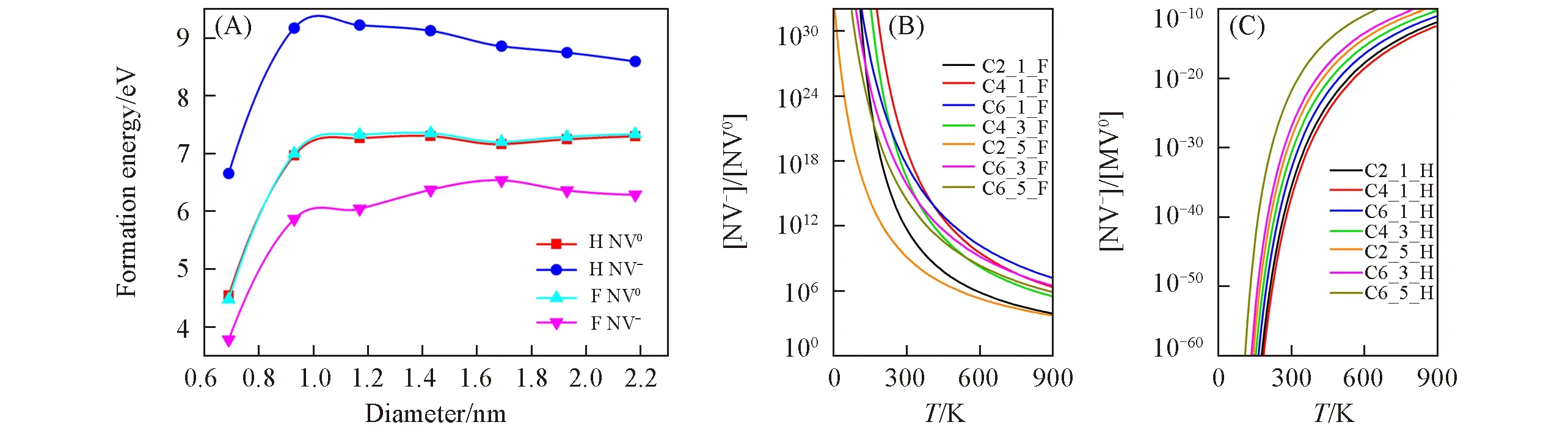
Fig.4 Formation energy(E form)of two NV centers(NV0 and NV-)doped in hydrogenated(H)and fluorinated(F)DNs(A),and[NV-]/[NV0]ratio in fluorinated(B)and hydrogenated DNs(C)as a function of temperature
As we know,the ratio of the concentration of NV-and NV0strongly depends on the formation energy difference[ΔE=Eform(NV-)-Eform(NV0)],which can be computed according to the Arrhenius equation

wherekis the Boltzmann constant andTis the temperature.For hydrogenated DNs,ΔE>0,whileΔE<0 for fluorinated DNs.The temperature-dependence[NV-]/[NV0]ratio is calculated and plotted in Fig.4(B)and(C).The results demonstrate that NV-center is easier to be created in the fluorinated DNs while NV0center is quite easily formed in the hydrogenated DNs.Thus,the NV-center is more stable than NV0in fluorinated DNs,but it is less stable than NV0with the hydrogenated surface.That is why a[NV-]/[NV0]ratio inversion can be observed experimentally in nanodiamonds when changing surface terminations[27―31].Moreover,when the diameters of DNs are increased to larger than 1.0 nm,theEformof NV centers are almost unchanged.Thus,it is a size-independent and long-range effect on the stability of NV-center in DNs.
The physical mechanism underlying the stability of the NV-center doped in DNs affected by surface modifications and diameter sizes can be understood in terms of classical physical model based on the surface electric dipole layer[Fig.5(A)]induced by partially ionic bonds on the surfaces[59],which can generate an electric potential defined as


Fig.5 Electric potential jump produced by a surface electric dipole layer(A)and a cylindrical surface electric dipole layer(B)
wherepandεrepresent the electric dipole moment per unit area on the surfaces and the dielectric constant,respectively.As shown in Fig.5(B),DNs can be considered as a cylindrical surface electric dipole layer,which can generate a size-independent electric potential jump inside cylindrical DNs calculated as[33,34]

Such size-independent electric potential jumps induced by the surface modification of DNs are also well correlated to the energy shifts of their electronic band structures as shown in Fig.1.Thus,such cylindrical surface dipole layer can provide a nondecaying and long-range effect on the stability of charged defects,which is independent of the diameter and only depends on the electric dipole moment on the surfaces.Therefore,the surface modification has a strong effect on the formation energy of the NV-center doped in large-diameter DNs,but no effect on the NV0center doped in DNs due to its zero-charge feature.
3 Conclusions
In summary,we investigate the electronic structures and stability of the NV centers doped in DNs by using large-scale spin-polarized DFT calculations up to hundreds of atoms and demonstrate that intrinsic electronic properties of the NV centers doped in DNs are independent of their surface modifications and diameters,but the formation energies of NV centers are sensitive to these effects.Surface modification provides a novel way to control the stability of the NV centers doped in DNs.DNs with fluorinated surfaces are relatively more conducive to forming the NV-center in diamond compared with hydrogenated surfaces.This investigation is in a good agreement with the existing experiments and makes important contributions to the understanding of intrinsic properties of NV centers in diamond for applications such as quantum information processing.
This paper is supported by the National Natural Science Foundation of China(Nos.21688102,21803066),the Pioneer Hundred Talents Program of Chinese Academy of Sciences(No.KJ2340000031),the National Key Research and Development Program of China(No.2016YFA0200604),the Program Anhui Initiative in Quantum Information Technologies,China(No.AHY090400),the Strategic Priority Research Program of Chinese Academy of Sciences(No.XDC01040100),the Fundamental Research Funds for the Central Universities,China(Nos.WK2340000091,WK2060000018),the Research StartUp Grants(No.KY2340000094)and the Academic Leading Talents Training Program(No.KY2340000103)from University of Science and Technology of China.
The authors thank the Supercomputing Center of Chinese Academy of Sciences,the Supercomputing Center of USTC,the National Supercomputing Center of Wuxi,and Tianjin,Shanghai,and Guangzhou,the Sugon Supercomputing Center of Beijing,Hefei,and Kunshan.
猜你喜欢
原子与分子物理学报(2021年2期)2021-03-29
石材(2020年10期)2021-01-08
陶瓷学报(2019年5期)2019-01-12
材料科学与工程学报(2016年4期)2017-01-15
材料科学与工程学报(2016年2期)2017-01-15
超硬材料工程(2016年1期)2016-02-28
超硬材料工程(2016年1期)2016-02-28
安徽地质(2016年4期)2016-02-27
西华大学学报(自然科学版)(2015年3期)2015-07-18
读者欣赏(2014年6期)2014-07-03