Effects of substitution of group-V atoms for carbon or silicon atoms on optical properties of silicon carbide nanotubes∗
Ying-Ying Yang(杨莹莹), Pei Gong(龚裴), Wan-Duo Ma(马婉铎),Rui Hao(郝锐), and Xiao-Yong Fang(房晓勇)
Key Laboratory for Microstructural Material Physics of Hebei Province,School of Science,Yanshan University,Qinhuangdao 066004,China
Keywords: silicon carbide nanotubes,group-V doped,optical properties,first-principles theory
1. Introduction
The silicon carbide (SiC) nanomaterials have excellent mechanical, thermal, electrical, and optical properties,[1–4]and they have been widely used in electronic devices, optical devices, and other fields.[5–7]Therefore, they have attracted much attention of many scholars.[8–12]SiCNT is an important low-dimensional material, which not only has the excellent characteristics of SiC crystal, but also shows some unique characteristics of nanotubes.[13–17]The unique optical characteristics of semiconductor SiCNT provide the possibility for its applications in optoelectronic devices.[18–20]Therefore,since SiCNT was synthesized experimentally,[21,22]it has been widely used as a nano-optoelectronic device material with broad application prospects, and has been widely concerned by the researchers.[23,24]
As an important method to adjust material properties,the dopant effects on electronic and optical properties of semiconductors have been studied.[25–28]For SiCNTs, group-V elements are the donor dopants, so studying the optical properties of group-V elements-doped SiCNTs is of great significance in the applications of SiC nano-optoelectronic devices.In recent years, there have been many reports on the influence of dopants on the properties of SiCNTs. For example, In 2009, Baoet al.studied the effects of N-doping on the optical properties of zigzag SiCNTs. The studies showed that N-doping reduces the value of absorption peak and produces many new absorption peaks.[29]In 2014, Behzadet al. studied the effects of Ga-doping on the optical properties of zigzag SiCNTs. The optical studies based on dielectric function indicated that new transition peaks and a blue shift are observed after Ga-doping.[30]Khodadadet al.investigated the structural and electronic properties of Li-doped SiCNTs.The calculations demonstrated that the doping of Li atom changes some physical properties of pure bundled NT.Owing to charges transferring from Li to SiCNTs, the most significant effect of Li intercalation on the electronic band structure is the shift of Fermi energy.[31]In 2018, Gonget al. studied the effect of group-III doping on the optical properties of SiCNTs. The study results showed that group-III element doping increases the minimum dielectric constant value, thereby increasing the transmittance;at the same time,it also introduces weaker absorption and dispersion in the near-mid-infrared region, and as the diameter of the doped atoms increases, the response peak is blue shifted.[32]In 2001,Huuet al.used the shape memory synthesis method,and achieved the first reproducible synthesis of SiCNTs of different internal and external diameters.[33]In 2002, one-dimensional silicon carbon nanotubes and nanowires of various shapes and structures were synthesized via the reaction of silicon(produced by disproportionation reaction of SiO)with multiwalled carbon nanotubes(as templates) at different temperatures.[21]In 2013, Romainet al.fabricated SiCNTs by carburization in silicon nanowires.It was found that the TO peak and LO peak of SiCNTs are at 796 cm−1and 972 cm−1respectively, and the peak of LO is higher than that of TO peak, indicating that the sp2and sp3bonding configurations exist in SiCNTs.[22]
So far, most of the researches on the SiCNTs doped by group-III elements and group-V elements have focused on structural stabilities, electrical, magnetic or optical aspects.However, most of these studies focus mainly on monatomic doping, and there are few reports on systematically studying the effect of a group of doping elements on the optical properties of SiCNTs. In this paper,the optical properties of SiCNTs doped by group-V elements(N,P,As,and Sb)are systematically studied by using the first-principles, and the optical differences and their effects caused by different substitutions are elaborated theoretically. These studies are of important significance in developing SiCNT nanodevices and putting them into practical applications.
2. Methods and models
Optimization of SiCNTs using CASTEP code was based on first-principles of density functional theory, and the optimization parameters were selected to be the same as those in Ref. [34]. The exchange correlation effect of the interaction between electrons were described by the Perdew–Burke–Ernzerhof(PBE)functional under the generalized gradient approximation(GGA),the plane wave cut-off energy was set to be 330 eV.[35]All the geometries were optimized by using the ultrasoft pseudopotentials until the force on each atom was less than 0.03 eV/˚A.All atomic geometry optimizations were performed in the first Brillouin zone,kgrid points were 1×1×6.
The supercell was constructed with twice the minimum unit of the armchair-type(6,6)SiCNTs. In order to reduce the influence of other SiCNTs, a vacuum layer thicker than 10 ˚A was added outside the supercell, and the optimized model is shown in Fig.1(a).
Based on this model, the C atoms (marked as NC-, PC-,AsC-, and SbC-SiCNTs) and Si atoms (marked as NSi-, PSi-,AsSi-,and SbSi-SiCNTs)at the same site of SiCNTs were replaced with group-V elements(N,P,As,Sb). Their optimized models are shown in Figs.1(b)and 1(c).
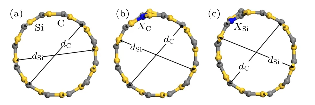
Fig. 1. SiCNTs and their doped SiCNTs structure models, showing (a)undoped SiCNTs, and [(b), (c)] SiCNTs where C atoms and Si atoms are replaced with group-V elements, with X representing group-V elements(X =N, P, As, and Sb), dC denoting diameter between the C atoms, and dSia referring to diameter between the Si atoms all in unit of ˚A.
3. Results and discussion
3.1. Structural stability
The optimized results are shown in Tables 1 and 2,wheredSianddCare the diameters of Si tube and C tube respectively, and the difference between their values is denoted by∆d=dC−dSias shown in Fig. 1. It can be seen that in the optimized SiCNTs,Si atoms are on the inside and C atoms are on the outside, and the tube wall thickness of SiCNT is not equal to zero(The wall thickness is about 0.1 ˚A).Obviously,unlike CNTs,in addition to sp2bonding configuration,SiCNT also has an sp3bonding configuration. In this paper,although the SiCNT model is sp2bonding configuration during modeling,there are both sp2bonding configuration and sp3bonding configuration after optimization, which is consistent with the experimental results.[22]

Table 1. Optimized structural parameters of SiCNTs with group-V atoms substituting for C atoms.

Table 2. Optimized structural parameters of SiCNTs with group-V atoms substituting for Si atoms.
The stability of doped SiCNT structure can be evaluated by the binding energy (or cohesive energy),[36]which is expressed as

whereETrepresents the total energy of doped SiCNT,NSi,NC,NXdenote the atom numbers of Si, C, and dopant (N, P, As,and Sb), andµSi,µC,µXrefer to the chemical potentials of Si, C, and doping atoms, where the values ofµSiandµCare−101.52 (Si),−145.84 (C), respectively. When C (or Si) in SiCNT is replaced,the formation energy can be expressed as

3.2. Optical absorption and photo-induced carriers
Figures 2(a)and 2(b)show the absorption spectra of SiCNTs in the band range of 60 nm–1500 nm after group-V atoms have replaced C and Si atoms, respectively. showing obviously that the differences among effects on optical absorption of SiCNTs in the band range of 60 nm–600 nm by doping different elements are almost negligible. In the frequency band between 600 nm and 1500 nm, there are obvious differences among the optical absorptions of the SiCNTs doped by different elements. From Figs.2(c)and 2(d),the absorption coefficient of NC-, PC-, AsC-, and SbC-SiCNT increase slowly, on the contrary,the absorption coefficient of NSi-,PSi-,AsSi-,and SbSi-SiCNT decrease.Especially for N-and P-doped SiCNTs,the absorption coefficient of NSi-SiCNT is about 5000 cm−1,larger than that of NC-SiCNT.
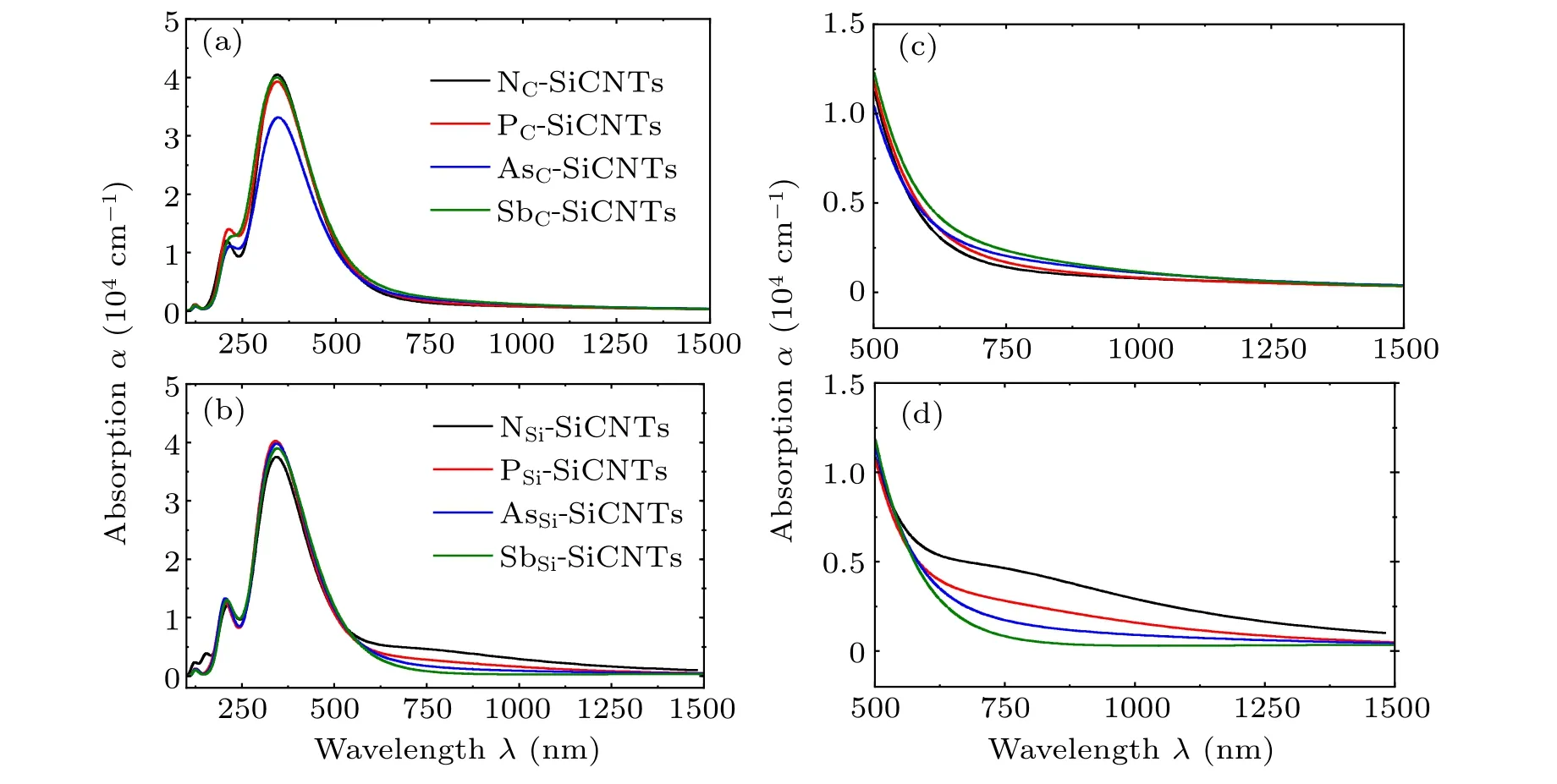
Fig. 2. Optical absorption spectra of SiCNTs where (a) C atom and (b) Si atom are replaced with group-V elements, and [(c), (d)] part of them in a range of 500 nm–1500 nm are magnified.
According to the Tauc equation,the optical absorptionαof SiCNT and its energy band structure satisfy the following relationship:[39]

whereAis a constant andhνis the photon energy. For a direct band gap semiconductor,r=0.5;for indirect band gap,r=2.Since group-V element-doped SiCNT is still of indirect band gap,r=2. The impurity concentration of doped SiCNT is denoted byNd,and the values for different SiCNTs are shown in Tables 1 and 2. The volume of SiCNT changes little for different doping elements and their displacements, so the impurity concentration does not change much, of them, the impurity concentration of AsC-SiCNTs is the lowest.Figure 2(a)shows that AsC-SiCNT has a minimum absorption peak, which is caused by the lowest impurity concentration of AsC-SiCNT.According to Fig. 2 and Eq. (3), Tauc fitting was performed for the doped SiCNT photoelectron energy level transition,the process and results are shown in Fig.3 and Table 3.
Figure 4 shows the band structure of doped SiCNTs,calculated based on the first-principles, whereEcis the conduction band bottom,EV1andEV2are the top and bottom of the upper valence band, respectively,EV3is the top of the lower valence band, andED1,ED2, andED3are the impurity levels.Their data are shown in Table 3.
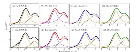
Fig. 3. Tauc fitting of doped SiCNTs, with [(a), (b), (c), and (d)] N, P, As, and Sb substituting for C atoms, and [(e), (f), (g), and (h)] N, P, As and Sb substituting for Si atoms.

Table 3. Electronic(characteristic)parameters of the doped SiCNTs.
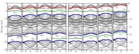
Fig.4. Energy band structure of SiCNTs with C atoms replaced by(a)N,(b)P,(c)As,and(d)Sb,and Si atoms replaced by(e)N,(f)P,(g)As,and(h)Sb substituting for Si atoms,respectively,and the Fermi level EF=0.
As can be seen from Fig. 4 and Table 3, when group-V element replaces a C atom, two impurity levels appear in the band-gap of SiCNT: the impurity near the bottom of the conduction band has smaller ionization energy,which belongs to the donor level, and the impurity is easy to form ionized donors; the other impurity level is near the Fermi level, because the ionization energy is larger, the number of electrons provided for the conduction band are much smaller than for the donor level. Most of the unionized impurities are in deep impurity level,and they can be regarded as a recombination center(or trap). When group-V element replaces a Si atom,only one impurity level appears near the Fermi level,the ionization energy is large,and it can also be regarded as a recombination center.
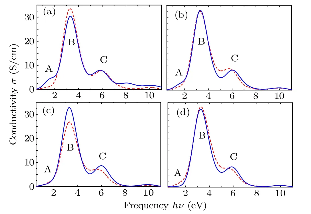
Fig. 5. Photoconductivity spectra of (a) N-, (b) P-, (c) As-, and (d) Sb-SiCNTs,respectively,with dotted line representing substitution of group-V element for C atom,and solid line denoting substitution of group-V element for Si atom.
Figure 5 shows the photoelectric spectra of SiCNTs after C and Si atoms have been replaced by group-V elements,which are mainly composed of three spectral regions A, B,and C. Among them, in the frequency band between 248 nm and 620 nm (B region), doped SiCNTs show a greater photoconductivity. This is because the valence band electrons absorb photons with energy greater thanEg(frequencyv >Eg/h)and then transfer to the conduction band, thereby generating photo-generated electrons and holes(non-equilibrium carriers). For group-V element-doped SiCNT, the lifetime of photo-generated carriers is on the order of ns, which is much longer than the photon period (corresponding to a frequency of about 1014Hz). Therefore, the photoconductivity generated by the intrinsic excitation of doped SiCNT presents a spectrum width corresponding to a frequency of about 2×10¹⁴Hz. In the case where group-V element substitutes for C atom, the conductivity of AsC-SiCNT is the smallest because of its lowest impurity concentration and smallest carrier concentration.[36]Similarly, in the case where group-V element replaces Si atom,because the carrier concentration is the lowest,the conductivity of NSi-SiCNT is also the smallest.
It can be seen from Fig.4 that the valence band of SiCNT is composed of high part and low part, and the band gap between the two valence bands is about 3 eV.[40]According to the energy band fitting in Fig. 3, it can be judged that the photoconductivity of the 155 nm–248 nm band (C region) is derived from the electronic transition of SiCNTs in the high valence band and the low valence band. When Si atom is replaced, the group-V atom has little effect on the SiCNT valence band. Therefore, the photoconductivity in the C region is almost unchanged; while when C atom is replaced, the pelectron effect of P, As, Sb are enhanced,[36]resulting in a closer relationship between the B spectral band and C spectral band.
The differences among photoconductivities caused by different elements are mainly reflected within the wavelength band above 620 nm (A region), and their spectra are derived from electronic transitions in the conduction band of the impurity level. Among them,the electrons in the shallow impurity level will present the photogenerated carriers in the midinfrared region of 6.8µm–16.2µm. Therefore,the photoconductivity of the A region in Fig. 5 comes from the electrons in the impurity level at the Fermi level. Because the impurity level when C atom is replaced is split into deep part and shallow part, the electron concentration on the impurity level at the Fermi level is less than that in the substitution for Si atom, resulting in a slightly larger conductivity of NSi- and PSi-SiCNTs as shown in Figs. 5(a) and 5(b). In addition, because the ionization energy of Sb atom replacing Si atom is much larger than that of Sb atom replacing C atom, the conductivity of SbC-SiCNT is larger than that of SbSi-SiCNTs as shown in Fig.5(d).
3.3. Optical refractive index and electron displacement polarization
Figure 6 shows the dielectric spectra of SiCNTs doped with different elements. It can be seen that when the group-V element replaces C atom,the real peak and imaginary peak of the dielectric function of AsC-SiCNTs are the smallest.Within the band less than 600 nm, the dielectric function value of AsC-SiCNT is the smallest, and none of the dielectric functions of NC-,PC-,and SbC-SiCNTs are significantly different.Within the band above 600 nm, the imaginary part of the dielectric function increases with the doped atomic number increasing, and the real part of the dielectric function increases with the doped atomic number increasing except for the smallest AsC-SiCNT.When group-V element replaces Si atom,the peak value of the dielectric function real part increases with the the number of doped atoms increasing,and the peak shows a significant red-shift phenomenon.The peak value of the NSi-SiCNTs dielectric function imaginary part is the smallest,and the values of other doping conditions are similar. In a frequency band of 500 nm–870 nm,the real part of the dielectric function gradually increases as the doped atomic number increases,while when it is above 870 nm,the real part of the dielectric function gradually decreases with the atomic number increasing. Within the frequency band greater than 550 nm,the value of the dielectric function imaginary part decreases with atomic number increasing. When group-V element replaces Si atom the dielectric function has more obvious change than when group-V element replaces C atom, and the difference is manifested mainly in a frequency band greater than 500 nm.

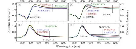
Fig.6. Dielectric spectra of doped SiCNTs,showing(a)real part and(b)imaginary part for group-V elements replacing C atoms,(c)real part and(d)imaginary part for group-V elements replacing Si atoms.

Fig.7. Refractive properties of doped SiCNTs,showing(a)refractive index and(b)extinction coefficient for group-V replacing C atoms,(c)refractive index and(d)extinction coefficient for group-V replacing Si atoms,respectively.
The dielectric spectrum of semiconductor follows the Lorentz model,and for the doped SiCNT containing multiple spectral peaks can be expressed as[41]

whereNandm∗are the electron concentration and the equivalent mass, respectively. The spectrum dielectric behavior of SiCNT is derived from free-electron plasma oscillation,τdenotes the relaxation time, and relates to the damping of the electron plasma oscillation. The oscillation frequencyωjdepends on the electron transitions between different bands. The refractive index of the semiconductor is determined by the electron displacement polarization. According to the electron polarization ratio model, the electron displacement polarization ratio of SiCNT can be expressed as[42]

whereMijdenotes the dipole transition matrix elements betweeniandjstates,andNrepresents the number of electrons in the transition.
According to the analysis of Fig. 2, Table 3, and Fig. 5,it can be seen that the two spectral peaks near 200 nm and 400 nm are derived from the transition between the valence band and the conduction band of SiCNT, respectively. Since there are few empty states in the valence band while many empty states in the conduction band,and the energy level difference in the valence band is greater than in the band gap,the dielectric constant and refractive index at 200 nm are much smaller than the values around 400 nm. Similarly,the number of free electrons of doped atoms is much smaller than the valence electrons of SiCNT,resulting in relatively low dielectric constant and low refractive index in the above 500-nm band.In particular,the differences among refractive indexes of SiCNTs,caused by different doping elements are reflected mainly in this frequency band, and their variation law is closely related to the concentration of free electrons in the donor ionization,which is consistent with the dielectric spectrum of Fig.6.As can be seen from Fig.7,the refractive index and extinction coefficient of AsC-SiCNT are the lowest because of its lowest impurity concentration.
3.4. Optical dispersion and loss
Dispersion and loss are important parameters to measure the optical properties of material. The dispersion coefficient can be expressed as[32]

whereλis the wavelength,cis the propagation speed of the electromagnetic wave in vacuum, andn(λ) is the refractive index of SiCNT. The dispersion spectra of SiCNTs doped by different elements are shown in Fig.8.
Figure 9 shows the reflectivity and loss factor of SiCNT doped with different elements. The loss factor is also called the loss tangent,which can be expressed as

whereε'andε''are the real part and imaginary part of the dielectric constant,δeis called the electrical loss angle.
It can be seen from Fig. 9 that except for the band near 300 nm, the reflectance of group-V element-doped SiCNT is less than 10%(10 dB),so it does not reflect visible light;NCSiCNTs has the largest refractive index when group-V element replaces C atom, followed by AsC-, PC-, and SbC-SiCNTs.When the group-V element replaces Si atom,the refractive index increases with the increase of the number of doping atoms in the band range of 400 nm–750 nm,and the situation is opposite in the band above 750 nm. Regardless of whether C or Si atom is replaced,the refractive index of SbC-SiCNT is the smallest.

Fig.8. Dispersion spectra of SiCNTs doped with(a)N,(b)P,(c)As,and(d)Sb respectively. It can be seen from Fig.8 that when group-V element replaces C atom,the dispersion coefficients of NC-and PC-SiCNTs are slightly larger than that of AsC-and SbC-SiCNTs,respectively,among them,AsC-SiCNT’s impurity concentration is the smallest and dispersion coefficient is the smallest. When group-V element replaces Si atom,there is no significant difference in the dispersion coefficient for doped SiCNT.When group-V element substitutes for Si atom,the dispersion coefficient is larger than that when C atom is replaced,but there is no big difference in the dispersion coefficient when N atom replaces C atom or Si atom.
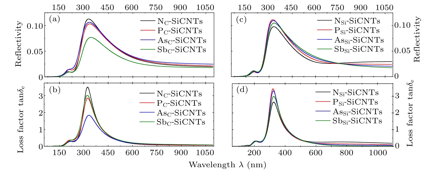
Fig.9. Reflectance and loss factorfor N,P,As,and Sb replacing[(a),(b)]C atom and[(c),(d)]Si atom.
Under optical frequencyε''=σ/ω, the loss comes mainly from the electronic conductance. When C atom is replaced, the loss of NC-SiCNT is the largest, and SbC-, PC-,and AsC-SiCNTs decrease in sequence;in the substitution for Si,the loss of NSi-SiCNT is the smallest,and SbSi-,AsSi-,and PSi-SiCNTs increase in sequence,which is similar to the trend of photoconductivity in Fig. 5. Whether C or Si atom is replaced, AsC-SiCNT has the least loss. By comparing Fig. 8 with Fig.9,it is clear that group-V element-doped SiCNT has a large loss around 300 nm,however,it generates a higher reflection due to the lowest dispersion coefficient in this band.
4. Conclusions
In this work, we have studied the effect on the optical properties of SiCNT where C atom or Si atom is replaced by the group-V element. The results are shown below. In the frequency band between 600 nm and 1500 nm, there are obvious differences among the optical absorptions of different elements doped SiCNTs. Especially for N-and P-SiCNTs,the absorption coefficient of NSi-SiCNT is about 5000 cm−1larger than that of NC-SiCNT. In the range of 248 nm–620 nm, the doped SiCNT has a greater photoconductivity, and the photoconductivity generated by the intrinsic excitation of doped SiCNT is exhibited within a spectral width corresponding to nearly 2×10¹⁴Hz. In the band greater than 620 nm, there are differences in photoconductivity when group-V element replaces C atom or Si atom. When the group-V element replaces Si atom, the dielectric function and refractive index change significantly compared with when C atom is replaced,and the difference is manifested mainly in the frequency band above 500 nm.Regardless of whether C or Si atom is replaced,SbC-SiCNT has the smallest refractive index.
- Chinese Physics B的其它文章
- Quantum computation and simulation with vibrational modes of trapped ions
- ℋ∞state estimation for Markov jump neural networks with transition probabilities subject to the persistent dwell-time switching rule∗
- Effect of symmetrical frequency chirp on pair production∗
- Entanglement properties of GHZ and W superposition state and its decayed states∗
- Lie transformation on shortcut to adiabaticity in parametric driving quantum systems∗
- Controlled quantum teleportation of an unknown single-qutrit state in noisy channels with memory∗

