Band alignment between NiOx and nonpolar/semipolar GaN planes for selective-area-doped termination structure∗
Ji-Yao Du(都继瑶) Ji-Yu Zhou(周继禹) Xiao-Bo Li(李小波) Tao-Fei Pu(蒲涛飞)Liu-An Li(李柳暗) Xin-Zhi Liu(刘新智) and Jin-Ping Ao(敖金平)
1School of Automation and Electrical Engineering,Shenyang Ligong University,Shenyang 110159,China
2Institute of Technology and Science,Tokushima University,Tokushima,Japan
3School of Physics,Sun Yat-Sen University,Guangzhou 510275,China
Keywords: GaN,NiOx,band alignment,vertical diode
1. Introduction
Vertical GaN Schottky barrier diodes (SBDs) are attractive for power-switching application due to their intrinsic low turn-on voltage,high breakdown voltage in small area,no surface trap,and good thermal stability.[1–5]Especially,with the development of low threading dislocation density(104cm−2–105cm−2) free-standing GaN substrate, remarkable progress has been achieved over the past decades. However, the reported average breakdown electric field, which is the breakdown voltage divided by the thickness of the GaN drift layer,for GaN vertical SBD is usually smaller than 1 MV/cm,which is far below the theoretical value of 3 MV/cm.[6]Under reverse bias, the peak electric field in the vertical SBD will crowd at the Schottky contact anode/GaN interface, causing the premature breakdown at the edge of device. Therefore,terminal techniques are suggested as the compromising solutions to suppress the electric field crowding and improve the breakdown voltage.
Several kinds of edge termination techniques,[7–9]such as field plate, beveled MESA, guard ring, and junction barrier Schottky (JBS), have been proposed until now. Among those methods, selective-area-doping method for forming ptype layer plays an important role in guard ring (Fig. 1(a))and JBS (Fig. 1(b)) structures. The buried p-type region below Schottky anode forms a lateral pn junction and creates a potential barrier to shield the Schottky contact under reverse bias,which is effective in suppressing the electric field crowding. Generally, selective-area-doping for p-type GaN is realized through implantation and trench-filling-regrowth.[10–12]However, high temperature process is necessary for ion implantation to activate the Mg-dopant and remove the implantation damage, which results in the surface decomposition of GaN.[12]While for the regrowth route, the Mg-doped GaN should be grown onc-plane at the bottom of trench and on the nonpolar (or semipolar) plane at the sidewalls of trench simultaneously.[11]The discrepancy in growth mode for different planes yields a rough surface with non-uniform distribution of acceptors in p-GaN inside the trench.
Nickel oxide (NiOx) deposited by sputtering is a natural p-type semiconductor with a critical electric field of approximately 3.5 MV/cm,[13]which is comparable to the critical electric field of GaN. Besides, the relatively low deposition ratio provides a good trench-filling capability along with a flatten surface. Previously, we reported a vertical GaN diode with p-NiOxserving as planar guard ring termination,which can enhance the breakdown voltage obviously.[14]The band alignment between NiOxandc-plane GaN was measured by x-ray photoelectron spectroscopy(XPS),which plays a crucial role in determining the charge transport across the heterojunction.[15]Herein,we first determinate the band offset between NiOxand nonpolar GaN plane and between NiOxand semipolar GaN plane,which are beneficial to the fabrication of termination structures for vertical GaN diodes.
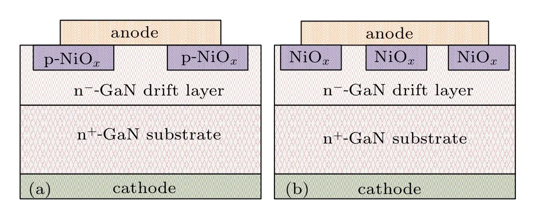
Fig. 1. Schematic view of vertical GaN diode (a) with NiOx guard ring termination structure,and(b)with junction barrier Schottky termination structure.
2. Experiments and characterization
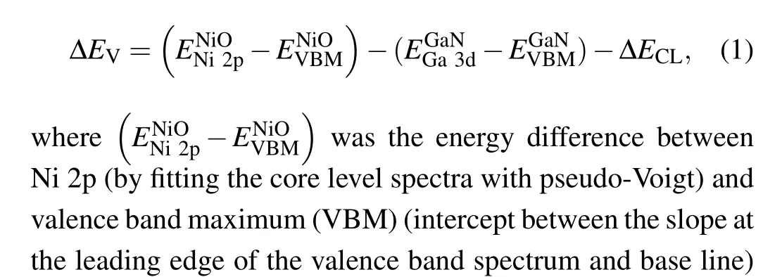
Three kinds of commercial free-standing GaN substrates(unintentionally doped with an electron concentration of 5×1017cm−3)were adopted for investigation. The surface crystalline planes werea-plane,m-plane, andr-plane, respectively. To measure the band offset, each substrate was cut into three pieces and coated with 0 nm-, 5 nm- and 50 nmthick NiOxfilms, respectively, by radio frequency (RF) magnetron sputtering. A NiO target with a high purity of 99.99%was used in our experiments. A mixture of argon and oxygen (Ar:O2=10:1) was introduced into the chamber with a pressure of 3 mTorr (1 Torr=1.33322×10²Pa). To eliminate the repeatability concern,we have optimized our experiment procedure. Firstly,the Ar:O2ratio presented a relatively low sputtering rate of approximately 0.83 nm/min. Secondly,for the same NiOxthickness, we placed three kinds of substrates into the chamber simultaneously. The band discontinuity was obtained by an XPS system(Thermo Fisher Scientific)with monochromatized AlKα(1486.60 eV)radiation source.The Fermi level edge and binding energy were calibrated using nickel metal and the C 1s peak of adventitious carbon(at approximately 284.80 eV), respectively. All the core level spectra were analyzed by pseudo-Voigt(mixed Lorentzian and Gaussian)fitting with Shirley background to determine the energy values. In the Kraut method it is assumed that the energy difference between the valence band edge and core level peak of the substrate is unchanged with the over layer.Then,the valence band offset(VBO,∆EV)is calculated from the following formula:

Based on our previous work, the band gaps of NiOxand GaN were 2.80 eV and 3.40 eV at room temperature,respectively,[16]
3. Results and discussion
3.1. Band alignment between NiOx and a-plane GaN
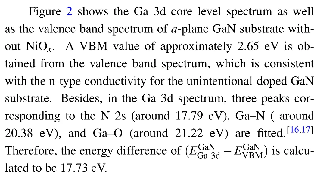

Fig. 2. Ga 3d and valence band spectrum for a-plane bulk GaN without NiOx layer.
The core level spectra of Ni 2p and valence band spectrum for 50-nm NiOxona-plane GaN are shown in Fig. 3.The obtained XPS signals are comparable to those of the NiOxbulk material,which means that a thickness of 50 nm is effective in eliminating the effect of GaN wafer. The VBM value of NiOxmeasured from the valence band spectra by using linear fitting is approximately 0.69 eV,implying the p-type conductivity characteristics. Besides, the Ni 2p spectrum is fitted to three peaks around 854.09 eV,855.70 eV,with a satellite peak at 861.04 eV. The former two peaks are assigned to Ni2+and Ni3+bonds as reported in previous work, implying that the grown film contains both NiO phase and Ni2O3phase. The satellite peak is usually attributed to various possible originations such as multi-electron excitation, multiple

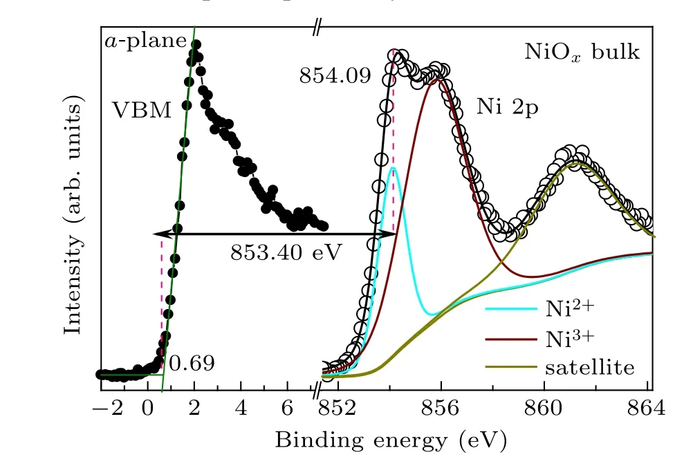
Fig.3. Ni 2p and valence band spectrum for the 50-nm NiOx deposited on a-plane bulk GaN.

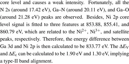
Fig. 4. Core level energy difference between Ga 3d energy levels of thin NiOx on a-plane GaN.

Table 1. Summary of band alignments between NiOx and different GaN planes.
3.2. Band alignment between NiOx and m-plane GaN


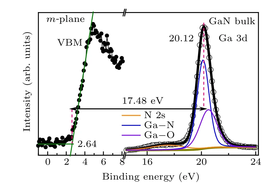
Fig. 5. Ga 3d and valence band spectrum for m-plane bulk GaN without NiOx layer.

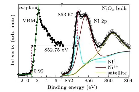
Fig.6. Ni 2p and valence band spectrum for 50-nm NiOx deposited on mplane GaN.
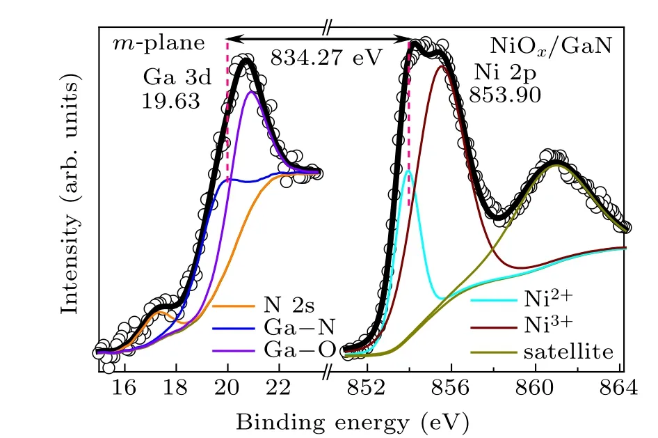
Fig. 7. Core level energy difference between Ga 3d energy levels of 5-nm NiOx on m-plane GaN.
3.3. Band alignment between NiOx and r-plane GaN
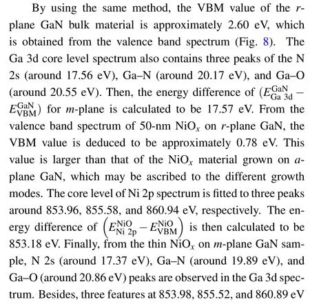

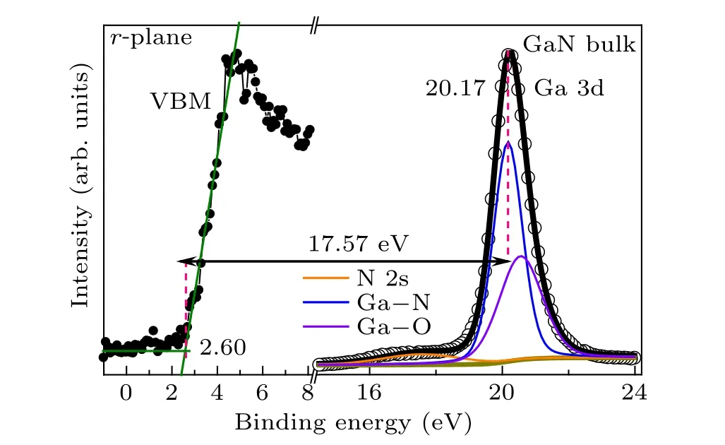
Fig.8.Ga 3d and valence band spectrum for r-plane bulk GaN without NiOx layer.
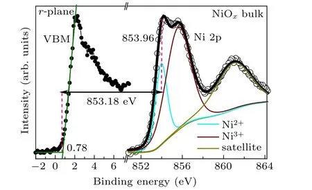
Fig. 9. Ni 2p and valence band spectrum for 50-nm NiOx deposited on rplane GaN.
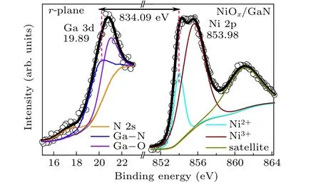
Fig.10. Core level energy difference between Ga 3d energy levels of 5-nm NiOx on r-plane GaN.
As summarized in Table 1, the valence band maximum values of thea-plane,m-plane,andr-plane GaN substrates are comparable to each other (approximately 2.65 eV), implying that the unintentional-doped substrates are of n-type with similar background electron concentration.However,the band offset at NiOx/GaN interface presents obvious crystalline plane dependency although it is coated with the same NiOxfilm.The polarization of GaN usually generates the charge on the surface and causes the band to bend. In our experiments, thea-plane and them-plane are nonpolar GaN planes while ther-plane is semipolar plane. Therefore, the band alignment of NiOx/a-plane or NiOx/m-plane should not be affected by the polarization charge. While for ther-plane,the negative charge on surface generates a band bending upward and reduces the band offset. None of those results is consistent with the XPS result as shown in Table 1. To understand the mechanism of this discrepancy,we fit the Ga 3d spectrum of the sample with 5-nm NiOxon GaN substrate. It demonstrates that the Ga–O/Ga–N ratio ofa-plane,r-plane,andm-plane GaN substrates are approximately 0.29,0.78,and 1.07,respectively. Combining the variation trend of the band offsets, we assume that a relatively high Ga–O content at the interface corresponds to a small band offset.[23]On the one hand,the high Ga–O content on GaN surface will change the growth mode of NiOx,resulting in a large VBM value. On the other hand,the large affinity of O than that of Ga will attract electron and generate a dipole at the interface,resulting in an extra energy band bending and the band offsets decreasing.
4. Conclusions
In this work, the band discontinuities between NiOxand nonpolar GaN plane and between NiOxand semipolar GaN plane are obtained by XPS with a Kraut method. The NiOxthin film deposited by sputtering presents a band gap of approximately 2.7 eV as well as a small amount of Ni2O3.Based on core-level binding energy and valence band maximum value,a type-II band alignment is formed at the interface between NiOxand nonpolar GaN plane and between NiOxand semipolar GaN plane. The VBO (CBO) values present obvious plane dependency and are 1.90 (1.30) , 1.00 (0.40), and 1.52 (0.92) eV for thea-plane,m-plane, andr-plane GaN,respectively. By fitting the Ga 3d spectrum obtained from NiOx/GaN interface, we find that relatively high Ga–O content at the interface corresponds to a small band offset. These results are beneficial to the selective-area-doped termination structure design of vertical GaN Schottky barrier diodes.
- Chinese Physics B的其它文章
- Quantum computation and simulation with vibrational modes of trapped ions
- ℋ∞state estimation for Markov jump neural networks with transition probabilities subject to the persistent dwell-time switching rule∗
- Effect of symmetrical frequency chirp on pair production∗
- Entanglement properties of GHZ and W superposition state and its decayed states∗
- Lie transformation on shortcut to adiabaticity in parametric driving quantum systems∗
- Controlled quantum teleportation of an unknown single-qutrit state in noisy channels with memory∗

