Effects of post-annealing on crystalline and transport properties of Bi2Te3 thin films∗
Qi-Xun Guo(郭奇勋) Zhong-Xu Ren(任中旭) Yi-Ya Huang(黄意雅) Zhi-Chao Zheng(郑志超)Xue-Min Wang(王学敏) Wei He(何为) Zhen-Dong Zhu(朱振东) and Jiao Teng(滕蛟)
1Department of Material Physics and Chemistry,University of Science and Technology Beijing,Beijing 100083,China
2Collaborative Innovation Center of Advanced Steel Technology,University of Science and Technology Beijing,Beijing 100083,China
3Beijing National Laboratory for Condensed Matter Physics and Institute of Physics,Chinese Academy of Sciences,Beijing 100190,China
4National Institute of Metrology,Beijing 100029,China
Keywords: topological insulator, magnetron sputtering, post annealing, Kiessig fringes, low carrier density,weak antilocalization
Three-dimensional topological insulators (TIs) like Bi2Te3have attracted considerable research attention on account of their unique energy band structure: they are insulating in the bulk and exhibit gapless metallic surface states. The nontrivial surface states of TIs have been confirmed by various methods such as angle-resolved photoemission spectroscopy experiments,[1–3]scanning tunneling microscopy/spectroscopy,[4]and transport measurements.[5]However,in most TIs,the bulk does not insulate and the Dirac point is not exposed or not close to the Fermi level, masking the topological phenomena. To utilize the unique electronic properties of the surface states, suppressing the contribution from the bulk is desirable in TIs-based electronic devices. Tremendous efforts have been made to reduce the bulk carrier density,such as using compensation doping with Sb or Se elements in Bi2Te3materials,[6,7]back gate, top gate, or dual gate modulation.[8–10]
Due to the hexagonal structure of bulk Bi2Se3, Bi2Te3,and Sb2Te3,it is common that thin films of TIs are composed of many triangular grains and each grain has terrace-step surface morphology.[11,12]At the center of the triangular grains,the film thickness is the largest,while at the grain boundaries,the thickness is the smallest.Therefore,TI thin films may have relatively large root-mean-square surface roughness.
To grow high-quality topological insulator thin films with low roughness and suppress the bulk carriers density, several methods have been used, including molecular beam epitaxy(MBE),[13,14]pulsed laser deposition (PLD),[15,16]chemical vapor deposition(CVD),[17]and magnetron sputtering.[18]As is well known, MBE growth allows for a precise control of the growth parameters to obtain a very low density of defects.However,MBE operates in ultra-high vacuum conditions and is significantly expensive. On the other hand,magnetron sputtering is highly versatile and a well-established method for growing a variety of TIs on a large scale, which is very important for industrial applications.
In our previous work,[18]we have successfully fabricated Bi2Te3thin films on 4 inches wafer by magnetron sputtering method. Here,we present a method of the heating process to obtain the high-quality Bi2Te3films with low carrier density down to 4.0×1013cm−2. For comparison, the Bi2Te3thin films were prepared by magnetron sputtering with two different heating processes:one is grown at a high substrate temperature, the other is grown at room temperature then followed by post-annealing. Structure analysis using x-ray diffraction(XRD), x-ray reflectivity (XRR), and scanning electron microscope (SEM) indicates that the latter process enables the growth of highly-oriented Bi2Te3thin films with larger grain size and smoother interface. Electrical transport properties show that lower carrier density and larger coherent length have been achieved in post-annealed Bi2Te3thin films. Our studies pave a way for Bi2Te3thin films to be integrated with magnetic multilayers and heterostructures for spintronic applications.
All of our samples were prepared by magnetron sputtering on silicon substrates(300 nm SiO2/Si). The co-sputtering method with high purity(99.99%)Bi2Te3alloying target and Te target was used to control films’ composition. Direct current (DC) power source was used for Bi2Te3alloying target and radio-frequency (RF) power source was used for Te target. The base pressure of the deposition chamber was below 3×10⁻⁷Torr and the working argon pressure was set at 2 mTorr. Films were deposited at room temperature and the substrate temperature was kept at 240◦C. All films were capped with a 4 nm thick Al thin film. The Al thin film was naturally oxidized to form AlOxafter exposure in air and to protect the TIs layer from oxidation. The post-annealing process was performed in a vacuum of 10−7Torr for 3 hours at various temperatures (200◦C, 240◦C, and 280◦C). XRD,XRR, and SEM were used to characterize the film structure.The transport properties were tested by the physical properties measurement system(PPMS)of the Quantum Design.
In Fig.1,we present the x-ray results of the prepared samples. As described in our previous report,[18]polycrystalline Bi2Te3thin films can be successfully grown at the substrate temperature of 240◦C.XRD spectrum of this sample is shown as the red curve in Fig. 1(a). We can see three peaks in this spectrum: (0 0 3),(0 0 6),and(0 0 15),showing the evidence of preferred growth with ac-axis orientation. We can also see that there is no obvious peak in the curve of the Bi2Te3film grown at room temperature, indicating an amorphous phase.However,after annealing at 200◦C for 3 hours,the characteristic peaks of(0 0 3n)appeared,suggesting that the amorphous sample transformed into the crystalline phase after annealing.The full-width at half-maximum (FWHM) of (0 0 6) of the film annealed at 200◦C is about 0.6◦,smaller than 0.9◦of the substrate-heated sample. When the annealing temperature increased to 280◦C, the characteristic peaks still exist and the FWHM is nearly constant at 0.6◦. The smaller FWHM, or sharper diffraction peaks of the annealed samples than that of the substrate heated sample means that the post-annealed Bi2Te3films have a larger grain size and better crystallinity.Strong Kiessig fringes can be observed around the Bi2Te3diffraction peaks, as shown in the inset of Fig. 1(a), which originate from the interference of x-ray beams reflected at the substrate–film and film–air interfaces.[19]The occurrence of these well-shaped fringes confirms a uniform and smooth surface and high crystal quality of the annealed Bi2Te3films.
Figures 1(b) and 1(c) show measured XRR data (black dots)of the substrate-heated and 280◦annealed Bi2Te3films.For the substrate-heated sample (Fig. 1(c)), the XRR curve shows a monotone decrease,while for the post-annealed sample(Fig.1(d)),continuous oscillation(Kiessig fringes)can be observed. By the deepness of Kiessig fringes, we conclude that the substrate-heated Bi2Te3film has a much larger roughness while the post-annealed Bi2Te3film has a better interface and lower roughness, which is consistent with the results obtained from XRD.Besides,the thickness of the post-annealed Bi2Te3film is determined to be 13.8 nm by using the GenX software.[20]
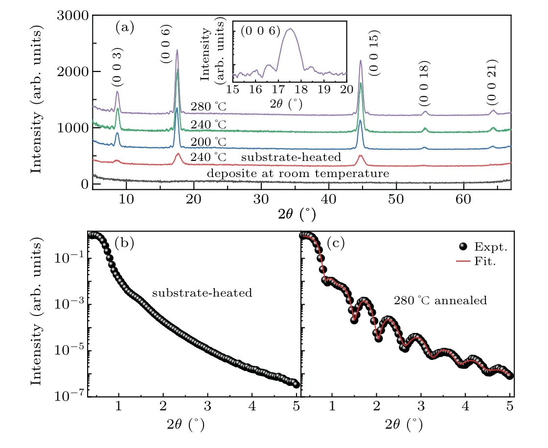
Fig.1.XRD and XRR spectra of the Bi2Te3 films.(a)XRD spectra of Bi2Te3 films for different substrate temperatures(room temperature and 240◦C)and different annealing temperatures (200 ◦C, 240 ◦C, and 280 ◦C). The inset shows a fine scanned image of the BT film annealed at 280 ◦C between 15◦and 20◦. XRR spectra of the substrate-heated (b) and 280 ◦C annealed(c) Bi2Te3 films. The black dots are measured data, and the red line is the fitting curve.
Figure 2 shows SEM images of surface morphologies of Bi2Te3films with different heat treatment processes. It can be seen that the surface of the as-deposited film(Fig.2(a))is quite flat, while the surface of the 280◦annealed film (Fig. 2(c))is rougher, indicating that annealing causes the growth of the grains. The film sputtered at high substrate temperature has flaky or granular morphology and is formed by grains of Bi2Te3nanoplates with different sizes(Fig.2(b)). In this image,we notice that many Bi2Te3nanoplates are not parallel to the surface of the substrate,which may be responsible for the broader peaks of XRD pattern of the substrate-heated sample.
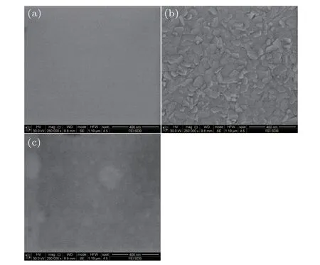
Fig.2.SEM images for Bi2Te3 thin films sputtered at room temperature(a),sputtered at the substrate temperature of 240 ◦C(b),and sputtered at room temperature then followed by annealing at 280 ◦C(c).
The transport measurements were carried out in the standard Hall bar geometry. Figures 3(a) and 3(c) are the Hall curves (Rxy–H) of the substrate-heated and 280◦C annealed Bi2Te3films, respectively. The Hall slopes of both samples at 2 K and 300 K are negative, which clearly reveals that the dominant carriers of both samples are electrons. Figures 3(b)and 3(d)show the temperature-dependent nominal carrier density of two samples estimated fromRxy. At 2 K, the carrier density is 13.5×1013cm−2for the substrate-heated sample and is 4.0×1013cm−2for the 280◦C annealed sample.The carrier density of the substrate-heated sample is about 3.4 times larger than that of the 280◦C annealed sample. It indicates that the carrier from bulk is largely suppressed in the 280◦C annealed Bi2Te3thin films.
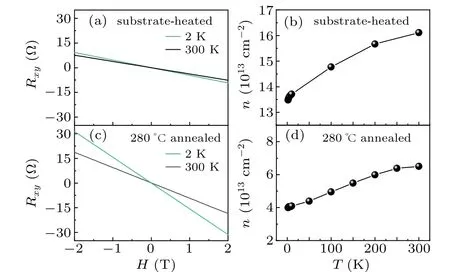
Fig.3. Hall curves of substrate-heated(a)and 280 ◦C annealed(c)samples at 2 K and 300 K, respectively. Carrier density of substrate-heated (b) and 280 ◦C annealed(d)samples as a function of temperature.
Figure 4 shows sheet conductanceσxx(σxx=Rxx/(R2xx+R2xy))of the above two Bi2Te3thin films measured at various magnetic fields in the temperature range of 2 K to 10 K. A well-defined linear lnTdependence ofσxxis observed at low temperatures(solid lines are the linear fits). The slope ofσxxis defined byκ=(πh/e2)dσxx/dlnT.[21]As shown in the inset,κincreases with increasing magnetic field and is approximately unchanged when the magnetic field ranges from 0.5 T to 2 T. The sharp increase at low magnetic fields can be attributed to the rapid suppression of the weak antilocalization(WAL)effect,and the saturated value ofκin a high field range of 0.5–2 T suggests that the effect is quenched. At the high magnetic field, the saturatedκis ascribed to the contribution of electron–electron interaction(EEI).[22,23]Interestingly, the ratio of saturatedκof these two Bi2Te3thin films is very close to the ratio of the carrier density,3.4,which suggests that the strength of EEI is proportional to the carrier density.
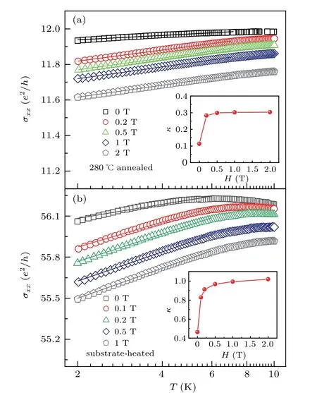
Fig. 4. Temperature dependencies of sheet conductance σxx (open symbols) recorded at different magnetic fields for (a) 280 ◦C annealed and(b) substrate-heated Bi2Te3 thin films. The straight lines are linear fits of σxx to lnT. Inset of each plot shows the slope κ =(πh/e2)dσxx/dlnT as a function of magnetic field.
To further explore WAL behavior,the magnetic field dependent sheet resistance was measured at varied temperature. Figure 5(a) shows the magnetic field dependence of∆Rxxof the post-annealed sample at different temperatures.The parabolic ∆Rxxcurve at the high-temperature region(50–250 K) is ascribed to a semiclassical model that conduction electrons drift in a magnetic field and are deflected by the Lorentz force. At the low temperatures (2–10 K), the ∆Rxxcurve is nearly linear at the high magnetic field, and a sharp dip appears near the zero magnetic field, which is a typical feature of the WAL effect. As shown in Fig. 5(b), the WAL behavior at the low magnetic field region(less than 0.5 T)can be well fitted by Hikami–Larkin–Nagaoka(HLN)equation[24]

whereαis the WAL coefficient,lϕis the phase coherence length, andψ(x) is the digamma function. It should be noted that, for the magnetic field larger than 0.5 T, the magnetoconductance is found to deviate from the HLN equation, and this is consistent with the results ofκbeing saturated above 0.5 T. Fitting ∆σxxat 2 K with the HLN equation yieldslϕ ∼228 nm and 180 nm for the 280◦C annealed and substrate-heated Bi2Te3thin films, respectively. Both values are much larger than the thickness of the films(14 nm), justifying the two-dimensional WAL characteristics in our samples. The temperature dependence oflϕof the two Bi2Te3thin films is shown in Fig. 5(c).It is clear that bothlϕdecrease with the temperature increasing from 2 K to 10 K and this monotonous reduction of coherence length was also observed in other topological insulator systems.[25,26]It is well-known that the coherence lengthlϕis proportional toT−1/2for the two-dimensional system.[27]Here,the power exponents of the two samples are−0.58 and−0.63(Fig.5(c)),slightly differ from−1/2,suggesting a contribution of the bulk channel. Anyhow,the long phase coherence length encourages us to take its advance in the quantum transport.
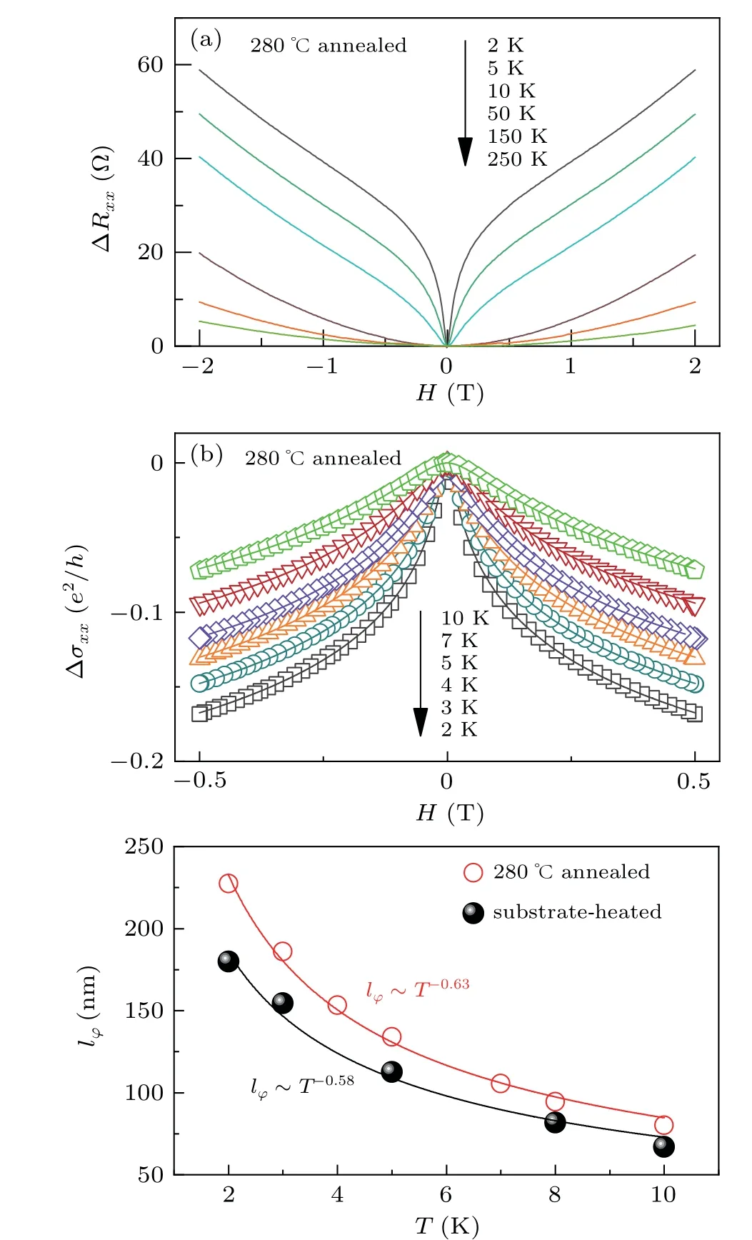
Fig.5. (a)The ∆Rxx of post-annealed sample as a function of magnetic field at different temperature,∆Rxx =Rxx(H)−Rxx(0). (b)Longitudinal conductance ∆σxx of post-annealed sample as a function of magnetic field at different temperature, ∆σxx =σxx(H)−σxx(0). The solid lines show the fit of HLN equation. (c) Phase coherence length lϕ of substrate-heated and postannealed samples as a function of temperature.
It has been shown in this study that the post-annealing Bi2Te3thin films have lower bulk carrier density than the films grown at high substrate temperatures. We note that the achieved carrier density is also lower than the values of samples grown by MBE,[13,14]PLD,[15,16]and CVD.[17]In previous studies, the bulk charge carriers of Bi2Te3mostly originate from point defects like TeBiantisite donor defects.[29,30]Thus, we can infer that the number of TeBiantisite defects in the 280◦C annealed samples is smaller than that in the substrate-heated samples. More detailed annealing processes,such as refining the annealing temperature and annealing time,than those used here would be necessary to find the best condition for further reducing the bulk carrier density of Bi2Te3thin films. Besides,more microstructure characterizations are needed to reveal the relationship between carrier density and the heat treatment process of Bi2Te3thin films.
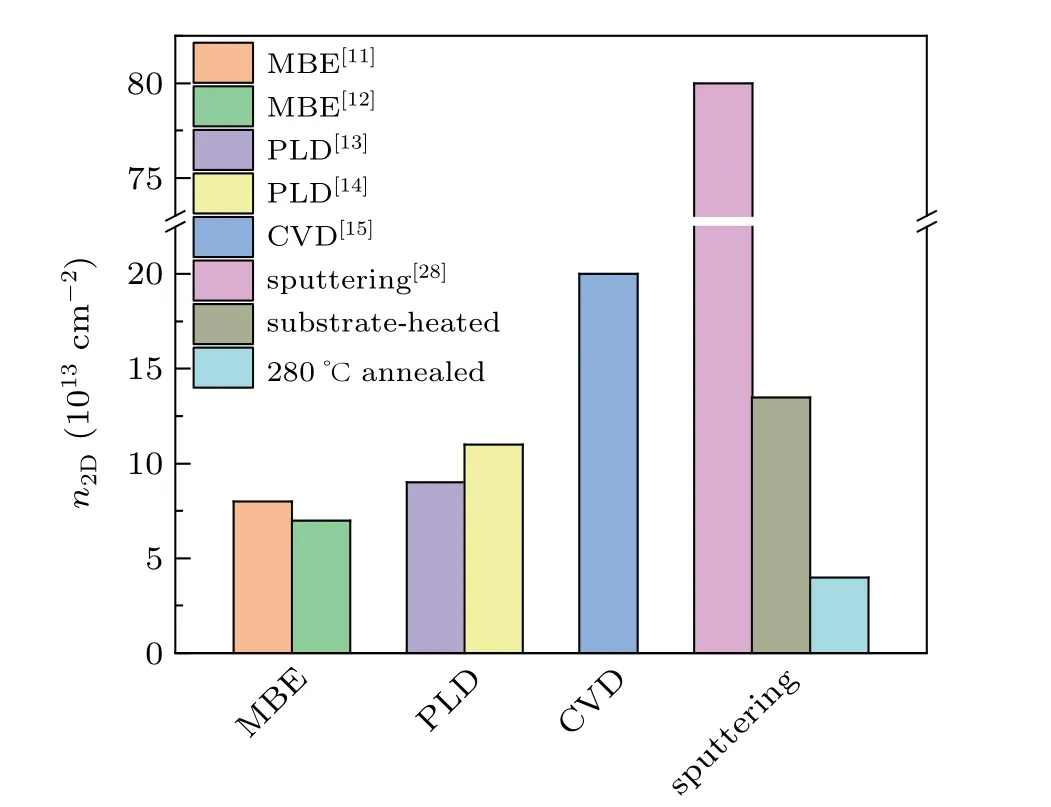
Fig.6. Comparison of our carrier density of Bi2Te3 thin films with previous reported data.
In conclusion,we present a feasible and scalable method based on magnetron sputtering to obtain high-quality Bi2Te3films,which was firstly sputtered at room temperature and then followed with post-annealing. It enables the growth of highlyoriented Bi2Te3thin films with larger grain size and smoother interface. The results of electrical transport show that it has a lower carrier density down to 4.0×1013cm−2as well as a larger coherent length up to 228 nm. The appearance of the WAL effect and EEI in our sample indicates that it keeps the character of the topological surface state. This work facilitates the fabrication of TI-based devices for electronic and spintronic applications.
- Chinese Physics B的其它文章
- Quantum computation and simulation with vibrational modes of trapped ions
- ℋ∞state estimation for Markov jump neural networks with transition probabilities subject to the persistent dwell-time switching rule∗
- Effect of symmetrical frequency chirp on pair production∗
- Entanglement properties of GHZ and W superposition state and its decayed states∗
- Lie transformation on shortcut to adiabaticity in parametric driving quantum systems∗
- Controlled quantum teleportation of an unknown single-qutrit state in noisy channels with memory∗

