Dynamic modulation in graphene-integrated silicon photonic crystal nanocavity∗
Long-Pan Wang(汪陇盼) Cheng Ren(任承) De-Zhong Cao(曹德忠)Rui-Jun Lan(兰瑞君) and Feng Kang(康凤)
1School of Opto-Electronic Information Science and Technology,Yantai University,Yantai 264005,China
2Wenjing College,Yantai University,Yantai 264005,China
Keywords: graphene,photonic crystal nanocavity,tunable
1. Introduction
Electro-optic modulators and switches are fundamental devices in optoelectronic integrated circuits.[1–4]Meanwhile,the most critical issue is whether the conversion of photoelectric signal can be realized effectively through modulators. Strong electro-optic modulation materials are needed to achieve compact and efficient modulators. Graphene,[5–8]a two-dimensional (2D) material with linear dispersion at the Dirac point,is an attractive candidate because of its excellent properties, such as tunable chemical potential and high carrier mobility,achieved by applying an electric field. Owing to these advantages,graphene can be used in integrated photonics based on silicon,[9–17]which is a promising candidate for on-chip data transmission. Through covering silicon devices with monolayer or multilayer graphene, tunable electro-optic modulators can be realized by the electrical gating of graphene by the use of an electrolyte.
In general, the size of electro-optic modulator based on silicon waveguide integrated with graphene[13–15]is relatively large because light needs to travel a considerable distance to realize the coupling of graphene with waveguide effectively.A planar PC nanocavity with a high quality factor is used to integrate with graphene to further enhance the light–matter interaction and reduce the size of the device.[18–22]Resonant modes can be strongly confined within the PC cavity region due to the effect of PC band gap. The evanescent field of resonant mode will strongly interact with the graphene layer when the silicon PC cavity is covered with graphene layer.Then,the modulation of cavity modes can be achieved by changing the electrical gating of graphene layer.
Majumdaret al.first realized the electrical control of the graphene–cavity system and about 2-nm shift of the cavity resonant linewidth was observed.[18]However, less than 1-nm shift of the resonant cavity mode was realized. Ganet al.reported a resonance wavelength shift close to 2 nm andQfactor modulation of more than 3 when integrating an air-slot PC nanocavity with graphene.[19]Three cavity modes were introduced in the near-infrared wavelength range, which reduced the free spectrum range (FSR). Chiba and Notomi proposed a reconfigurable nanocavity in a graphene-loaded silicon PC waveguide; a maximum resonant wavelength shift of about 0.5 nm was achieved.[20]
A large resonant wavelength shift can effectively reduce the restriction on the requirement of a high-Qcavity,i.e.a narrow linewidth of the cavity mode, which is conducive to resolving the two peaks before and after the modulator is excited by the electric field. Moreover, a large FSR means a single resonance in an ultra-wide band without being affected by adjacent resonances,which is especially attractive in an integrated wavelength division multiplexing system. Therefore,considering practical applications,the modulation wavelength shift and FSR must be maximized.
In this paper, we propose a high-Qacceptor-type PC nanocavity coupled with graphene layer in 2D silicon slabs.Through regulating the chemical potential of graphene, the resonance wavelength shift reaches 2.62 nm, which is a relatively large voltage tuning result compared with the findings reported thus far. A large modulation depth of 12.8 dB for the light reflection can also be obtained. TheQfactor can be reduced from the order of 104to about 300. Furthermore, only one resonant mode exists in the near-infrared band(1500 nm–
1640 nm),and a large FSR(131.59 nm)can be achieved.
The rest of this paper is organized as follows. In Section 2, we propose an acceptor-type PC nanocavity and then optimize its performance. Section 3 shows the modulation characteristics of the optimized nanocavity integrated with a graphene layer. Finally,Section 4 summarizes the study.
2. Design and optimization of PC nanocavity
The 2D triangular-lattice PC consists of circular air holes etched in a 220-nm thick silicon membrane on an insulator(SOI) wafer, whose process is compatible with the current complementary metal–oxide–semiconductor process. Meanwhile, the lattice constantais 450 nm, and the radius of air holes is 120 nm (0.267a). The refractive index of the membrane silicon is set to be 3.45 for the near-infrared light around
选择80例银屑病患者作研究对象,均为我院皮肤科2017年1月至12月收治。随机分组,中研究组40例中,男24例,女16例,年龄27-67岁,平均(47.45±11.32)岁;病程平均为(5.62±1.33)年;对照组40例中,男26例,女14例,年龄28-66岁,平均(47.37±11.25)岁,病程平均为(5.73±1.29)年。组间基线资金料可比(P>0.05)。
1550 nm. The well-established three-dimensional(3D)planewave expansion method is used to calculate the band structure of the above PC slab. In simulations,30 pixels per lattice constantatogether with periodic boundary conditions are used to ensure the calculation accuracy. The PC slab exhibits a
2D band gap of TE-like polarization ranging from 1402 nm to 1684 nm.
The traditional way to construct a defect cavity is to miss an air hole in the center of PC slab to realize a usual L1(missing one air hole) nanocavity. Then, six nearest-neighbor air holes around the defect column are eliminated,corresponding to an L7(missing seven air holes)nanocavity. This condition is equivalent to filling seven air holes with the background silicon. Subsequently,an air hole with radiusRais inserted in the center of L7 cavity, and an A1 cavity, which is an acceptortype cavity,is formed. Figure 1 shows the schematic of the A1 cavity.
The major difference between the A1 cavity and traditional L7 cavity lies in the occupation material within the center of the cavity. The material in the center of L7 nanocavity is silicon. On the contrary,the core of A1 nanocavity is air or infiltrated with other nonlinear materials. When the A1 cavity is in resonance,the resonant mode will have strong interaction with air or other nonlinear materials. Therefore,the A1 cavity may present a better modulation effect than traditional L-type cavity when the cavity is integrated with other nonlinear materials.
The highQfactor indicates that the nanocavity has good localizing characteristics to light, which is conducive to enhancing the interaction between the light field and material.Usually, theQfactor of the original A1 cavity is lower than that of traditional L3 cavity as described in Ref.[23]. Therefore,the A1 cavity needs to be optimized to achieve a moderateQfactor. The radiusRaof central air hole and the positions of neighboring holes around the cavity need to be changed to improve the performance of the A1 cavity.
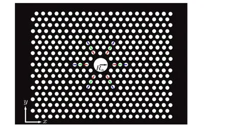
Fig.1. Schematic diagram of A1 cavity in triangular-lattice PC slab,where Ra is radius of central air hole,with red,green,and blue arrows representing the first, second, and third nearest-neighbor air holes along Γ–K direction,respectively,and arrows pointing to the direction of displacement.
As described in Ref. [24], changing the positions or shapes of air holes near the cavity edge can make the electric field profile of the cavity mode closer to the Gaussian function,thus obtaining a highQfactor for L3 cavity.However,the optimization of the A1 cavity needs to be further explored. Based on the above consideration, we first change the radiusRaof the central air hole to optimize the performance of A1 cavity.The 3D finite-difference time-domain(FDTD)combined with Pade approximation method is used to calculate theQfactor and resonant wavelength of the cavity. In simulations,30 pixels per lattice constantatogether with Berenger’s perfectly matched layer boundary conditions are used for ensuring the calculation accuracy. Point sources with broad spectrum are placed at the asymmetric positions in the cavity region to excite the cavity modes. Figure 2 shows the calculated results as a function of radiusRa. The black line with solid squares in Fig.2 shows the relationship betweenQfactor andRa,whereRais changed from 0.5ato 1.15a. TheQfactor first increases and then decreases with the increase inRa. WhenRaequals 0.917a,theQfactor of A1 cavity reaches a maximum value of 17232,achieving over four orders of magnitude.
With the increase inRa,the effective refractive index near the cavity region decreases. Thus,the resonant wavelength of the cavity moves to the short-wavelength range. The red line with solid circles in Fig. 2 shows the calculated relationship between the resonant wavelength andRa. The resonant wavelength is 1548.41 nm whenRais 0.917a. WhenRais changed from 0.764ato 0.987a, the resonant wavelength of the cavity can be located within a range of 1500 nm–1640 nm.
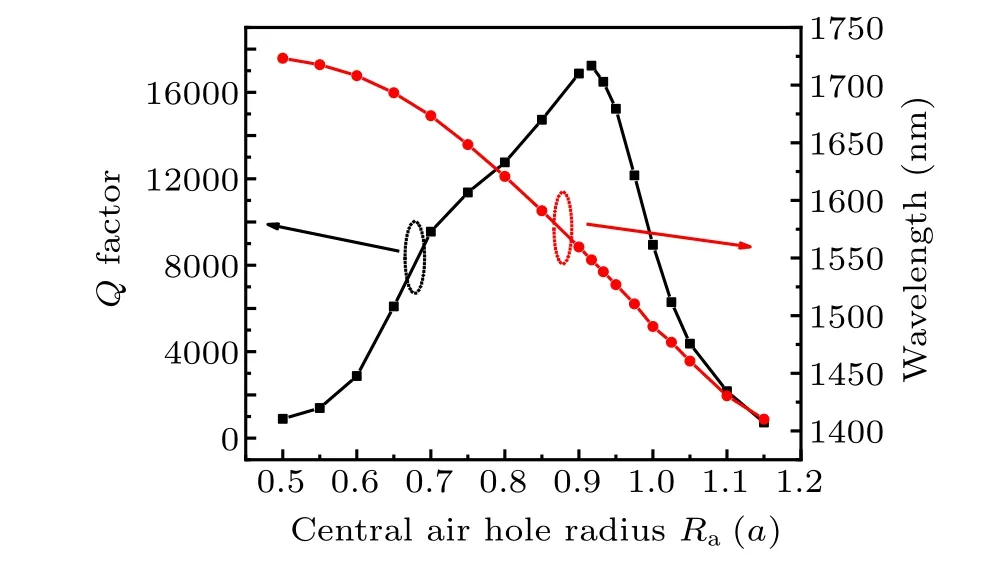
Fig.2. Calculated Q factor and resonant wavelength versus central air hole radius Ra.
Second, we displace the six air holes at positionA(the nearest neighbors)(red arrows in Fig.1)outwards in theΓ–Kdirection ranging from 0ato 0.30a. All the displacements are parallel to the lattice vector,whereasRa=0.917ais kept unchanged.Figure 3(a)shows the calculated results as a function of air hole shift. As the air holes are displaced outwards from 0ato 0.30a, theQfactor increases significantly and then decreases(black line with solid squares in Fig.3(a)). The maximumQfactor,which is as large as 26962,is obtained from the air hole shift at positionAof 0.05a. In Fig.3(a), the red line with solid circles represents the variation in resonant wavelength of A1 cavity. When the shift amplitude ranges from 0ato 0.30a,the resonant wavelength can be monotonically increased from 1548.41 nm to 1615.82 nm,and the wavelengthtuning magnitude can be increased up to 67 nm. The resonant wavelength of A1 cavity is 1566.44 nm when the peakQfactor is obtained for air hole shift of 0.05aat positionA.
Third,we shift the six air holes at positionB(the second nearest neighbors)(green arrows in Fig.1)inwards along theΓ–Kdirection from 0ato 0.30a. All the displacements are parallel to the lattice vector,with the air holes fixed at positionAat the optimal outward displacement of 0.05a. In Fig.3(b),the black line with solid squares and red line with solid circles correspond to the calculatedQfactors and resonant wavelengths,respectively.The maximumQfactor,which is as large as 29150,is achieved for the inward displacement of 0.05aof air holeB. Moreover, the resonant wavelength of A1 cavity is 1565.42 nm. Given that the air hole at positionBis at the periphery of the A1 cavity,displacement of air holeBhas less effect on the cavity mode than that of air holeA. Therefore,the wavelength shift is 4.8 nm.
Moreover,we shift the six air holes at positionC(the third nearest neighbors)(blue arrows in Fig.1)inwards in a manner similar to that ofB, with the positions of air holesAandBfixed at their optimal values,that is,outward 0.05aand inward 0.05a, respectively. The results are shown in Fig. 3(c). The maximumQfactor of 30171 is obtained for the displacement of air holeCof 0.20a.The corresponding resonant wavelength is about 1565.42 nm. In addition, when shifting the air holes at positionCinwards from 0ato 0.30a, the resonant wavelength of A1 cavity remains almost unchanged. This result may be caused by the location of air holes at positionCat the outer periphery of A1 cavity. Meanwhile, the movements of air holes have minimal effect on resonance wavelength.
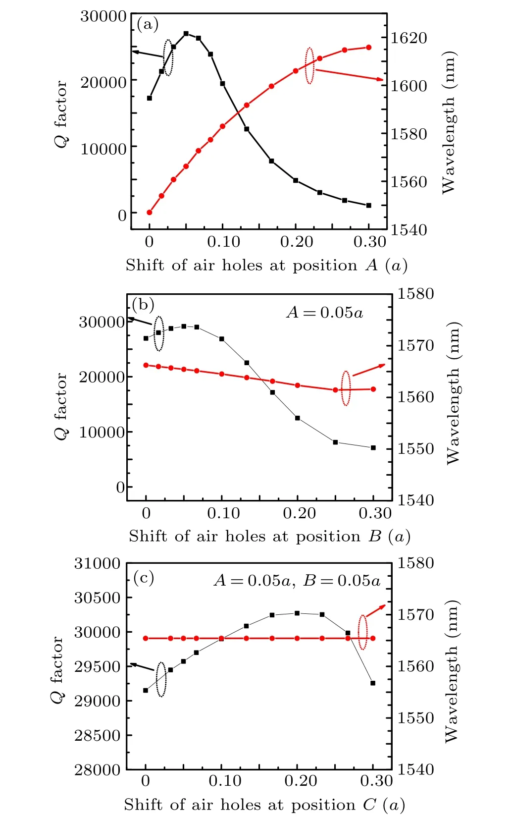
Fig. 3. (a) Q factors and resonant wavelengths obtained by FDTD simulations for A1 cavities with a range of displacements of air holes at(a)position A(the nearest neighbors),(b)position B(the second nearest neighbors)with the air holes fixed at position A at the optimal outward displacement of 0.05a,and(c)position C(the third nearest neighbors),with the positions of air holes A and B fixed at their optimal values, that is, outward 0.05a and inward 0.05a,respectively.
Figure 4 shows the electric field distribution of the optimized A1 cavity at 1565.42 nm. The red color represents the range with a strong amplitude,whereas the blue color denotes the range with a weak amplitude. It is shown in Fig. 4 that the electric field is mainly localized at the edge of the cavity,where strong interaction occurs when the nonlinear material is filled.
Although a considerably highQfactor can be obtained for the traditional L-type PC nanocavity,[25]the nanocavity with a moderateQfactor is necessary for modulation devices integrated with graphene,which can achieve a relatively large spectral bandwidth. TheQfactor of graphene-based PC nanocavity,measured by cross-polarized reflectivity measurement setup,is only several hundreds.[18,19]Therefore,the performance of the optimized A1 cavity is sufficient for the use in modulation devices integrated with graphene.
Moreover, in the whole photonic band gap (1402 nm–1684 nm) of TE-like polarization, two resonant peaks,1433.83 nm and 1565.42 nm, are observed for the optimized A1 cavity. Figure 5 shows the calculated transmission spectrum,in which a large FSR of 131.59 nm can be achieved. In the FDTD simulations,a broad spectrum Gaussian pulse with a width of 4ain theydirection is normally launched on the left side of the structure shown in Fig.1. The time evolution of the pulse is collected by a power detector with a wider width of 6aon the right side of the structure, and then transformed to the frequency domain by Fourier transform. Finally,the transmission spectrum shown in Fig.5 can be achieved by dividing the output power by the input power at each frequency. Other parameters are the same as those used in previous calculations.
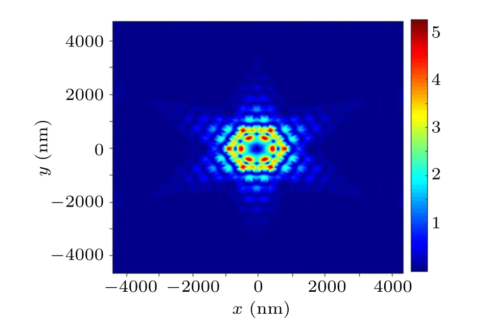
Fig.4. Electric field distribution of the optimized A1 cavity at wavelength 1565.42 nm, where red color represents the range with strong amplitude,and the blue color denotes the range with weak amplitude.
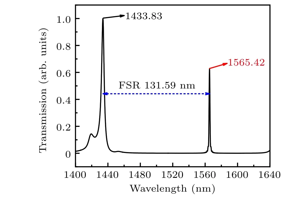
Fig. 5. Calculated transmission spectrum for structure shown in Fig. 1,showing two resonant peaks (1433.83 nm and 1565.42 nm) in the whole photonic band gap(1402 nm–1684 nm)of TE-like polarization.
3. Tunable PC nanocavity with single layer graphene
Graphene is a 2D crystal consisting of a single-layer carbon atoms and has intriguing optical absorption properties.The optical properties of graphene are directly related to its chemical potential, and its chemical potential can be controlled by applying a voltage to the graphene layer.[18,19]
The dielectric constant of graphene depends on the surface conductivity of single-layer graphene, which can be expressed as

whereσintraandσinterare the electrical conductivities determined by the intra-band transition and inter-band transition,respectively;ωis the angle frequency of light;ε0is the dielectric constant of vacuum;tis the thickness of graphene layer.
Based on Kubo formula, the graphene conductivity can be written as follows:[26]
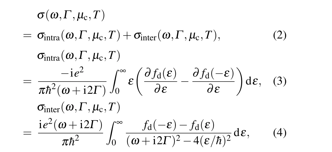
whereΓis the scattering rate,µcthe chemical potential, andTthe working temperature of graphene.
The Fermi–Dirac functionfd(ε) contains the chemical potential informationµc,which can be expressed as

Therefore, the dielectric constant and electrical conductivity of graphene can be tuned by changing the chemical potential. Figures 6(a) and 6(b) show the imaginary part and real part of electrical conductivity of graphene as a function of chemical potentialµc,which are shown by black line with solid squares and black line with solid circles, respectively.The real part of electrical conductivity represents absorption loss in a graphene layer. Figure 6(b) shows that the real part of electrical conductivity decreases gradually with the increase of chemical potential,corresponding to the reduced absorption loss of graphene. These are derived by assumingT=300 K andω=2πc/λ(λ=1550 nm).As for the scattering rateΓof graphene,we consider 100 fs,corresponding to a typical value for graphene at room temperature.
We use the monolayer graphene to cover the A1 nanocavity. Figure 7 shows the schematic diagram of electrically controlled graphene-PC nanocavity. Meanwhile, the drain,source, and gate electrodes of the graphene field-effect transistor(FET)are denoted as D,S,and G in Fig.7,respectively.The top magenta layer is the monolayer graphene.Underneath the graphene layer,is the air-bridge PC A1 nanocavity etched on 220-nm silicon membrane.This design can further enhance the coupling rate between graphene layer and A1 cavity modes because the cavity modes can experience more overlapping with the graphene layer than the traditional L3 cavity.
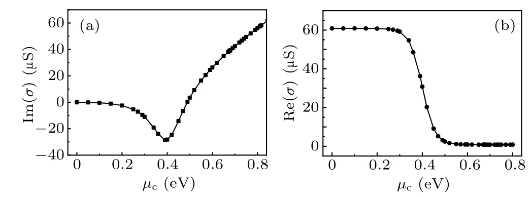
Fig.6. Calculated electrical conductivity of graphene as a function of chemical potential µc, with panels (a) and (b) representing imaginary part and real part of electrical conductivity,respectively.
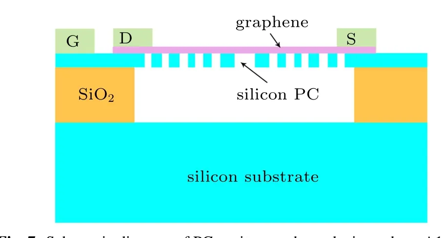
Fig.7. Schematic diagram of PC cavity–graphene device,where A1 cavity is fabricated on a 220-nm thick silicon membrane on SOI wafer, D,S,and G denote drain,source,and gate electrodes of graphene FET,respectively.
Based on the above theoretical analysis, the dielectric constant of graphene is a function of its chemical potentialµc. Therefore,the resonant wavelength of the A1 nanocavity covered with graphene can be tuned by adjusting the chemical potentialµcof graphene. The reflection spectra of the integrated structure are simulated with the FDTD method. In the simulations,a dipole source with broad spectrum is placed in the center of A1 nanocavity and a power detector in the outof-plane free space above the PC cavity is used to collect the emission power. The calculation parameters are the same as those used in the previous calculations. Figure 8 shows the resonant wavelength of the calculated reflection spectra when the chemical potentialµcchanging from 0 eV to 0.8 eV.
The resonant wavelength of the cavity can be divided into four ranges according to the changes in chemical potentialµc.In the first range, the change in resonant wavelength is extremely small, almost kept at about 1564.43 nm, when the chemical potential changing from 0 eV to 0.20 eV.In the second range, the resonant wavelength increases monotonically to 1565.3 nm,i.e.the wavelength shifts 0.87 nm, when the chemical potential is adjusted from 0.20 eV to 0.39 eV.In the third range, when the chemical potential is between 0.39 eV and 0.74 eV, the change in resonant wavelength shows complexity. The resonant wavelength decreases monotonically from 1565.3 nm to 1563.34 nm when the chemical potential increases from 0.39 eV to 0.6 eV. However, when the chemical potential changes from 0.6 eV to 0.74 eV, the resonance wavelength increases monotonically and then decreases to 1562.68 nm.Meanwhile,the resonant wavelength reaches a minimum value of 1562.68 nm when the chemical potential is 0.74 eV,i.e.,the wavelength shift can reach 2.62 nm when the chemical potential is in the third range (0.39 eV to 0.74 eV).Finally, when the chemical potential is tuned from 0.74 eV to 0.80 eV,the resonant wavelength can increase rapidly from 1562.68 nm to 1565.3 nm,i.e., the resonant wavelength shift is also 2.62 nm. Meanwhile,the resonant wavelength reaches a maximum value of 1565.3 nm when the chemical potential is 0.77 eV.In summary,the maximum tuning range of the resonance wavelength can reach 2.62 nm, which is a relatively large value for electrically tuned PC-cavity modulators to our knowledge. In addition, compared with the resonance wavelength of A1 cavity without graphene,the resonant wavelength of the cavity covered with graphene moves to a short value.
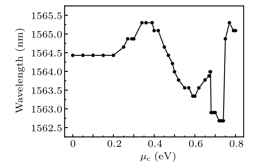
Fig. 8. Resonant wavelength of optimized A1 nanocavity integrated with single-layer graphene when chemical potential µc changing from 0 eV to 0.8 eV.
In addition, changing the complex dielectric constant or the real part of conductivity of graphene(which represents absorption loss in a graphene) can tune theQvalue of the A1 cavity covered with graphene. Figure 9 shows the calculatedQfactor as a function ofµcin a range from 0 eV to 0.8 eV.TheQfactor increases with chemical potentialµcincreasing,which corresponds to the gradual decrease of the real part of electrical conductivity of graphene shown in Fig. 6(b). The decreasing of absorption loss of graphene means that theQfactor of A1 nanocavity is improved.
Comparing with the resonance behavior of optimized A1 cavity without graphene, an evident degradation ofQfactor occurs due to the absorption of graphene layer. Two saturation-like ranges and a fast modulation range are observed in the whole range. In the first saturation-like range,i.e.,in a chemical potential range from 0 eV to 0.30 eV,theQfactor of the cavity increases slightly and stays at about 340.In the second saturation-like range,i.e.,in the chemical potential(µc)in a range from 0.55 eV to 0.8 eV,theQfactor shows a small fluctuation and is kept at about 1850. Meanwhile,the maximumQfactor is about 1892 when theµcis 0.65 eV.TheQfactor increases rapidly from about 340 to 1850 when the chemical potentialµcis in the fast-modulation range(0.30 eV to 0.55 eV). In the above region, the maximum modulation amplitude forQfactor can be in excess of 5.
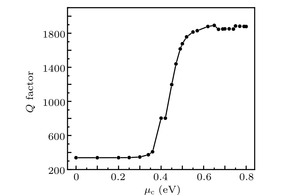
Fig. 9. The Q factor of graphene-PC cavity when changing the chemical potentialµc from 0 eV to 0.8 eV.
To better understand the modulation on cavity modes,we calculate the reflection spectra of A1 cavity integrated with graphene for different chemical potentials. Figure 10 shows the calculated results when the chemical potentials are 0.2,0.4, 0.5, 0.6, and 0.7 eV,corresponding to the magenta solid,black solid, green dashed–dotted, blue dashed, and red dotted lines,respectively. When the chemical potentials are equal to 0.7 eV and 0.6 eV, the peak reflectivity and linewidth of two cavity modes are similar except for the difference in resonant wavelengths, that is, 1562.76 nm and 1563.34 nm, respectively. However, when the chemical potentials are equal to 0.5 eV and 0.4 eV,which are located in the fast-modulation range, a significant broadening in the cavity linewidth and a decrease in the peak reflectivity can be observed with the decreased chemical potential of graphene. Simultaneously, the resonant wavelengths are 1563.99 nm and 1565.3 nm, corresponding to chemical potentials of 0.5 eV and 0.4 eV,respectively. In addition, when the chemical potential is equal to 0.2 eV, located in the first saturation-like range, the peak reflectivity decreases significantly. As depicted in Fig. 10, the modulation depth is as large as∼12.8 dB,when the chemical potential is changed from 0.7 eV to 0.2 eV.
Table 1 displays the comparisons of the proposed modulator based on A1 cavity with other PC modulators reported previously. As shown in Table 1,our designed modulator has the highest modulation efficiency in the several previously reported PC modulators.
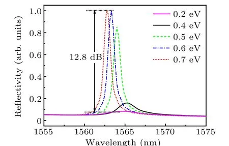
Fig. 10. Reflection spectra of graphene PC cavity when chemical potentials are 0.2,0.4,0.5,0.6,and 0.7 eV,corresponding to magenta solid,black solid,green dashed–dotted,blue dashed,and red dotted lines,respectively.

Table 1. Comparisons of proposed modulator with various PC modulators.
4. Conclusions
In summary,we have designed a novel acceptor-type A1 cavity in 2D silicon PC slabs. TheQfactor can achieve over four orders of magnitude, which is conducive to producing a strong interaction between cavity mode and other material.Through changing the chemical potential of graphene on the top of A1 cavity, the resonant wavelength can be tuned from 1562.68 nm to 1565.30 nm,i.e., the maximum wavelength shift is about 2.62 nm. Moreover,theQfactor can be changed from a peak value of 1892 to about 340, and the maximum modulation factor exceeds five due to the strong optical modulation.Therefore,the resonant wavelength andQfactor can be strongly tuned simultaneously for our proposed A1 cavity with a moderateQfactor. This work shows that such a graphenecavity-based modulator can be used for implementing the fast and intense electro-optic modulation in integrated silicon photonic applications.
- Chinese Physics B的其它文章
- Quantum computation and simulation with vibrational modes of trapped ions
- ℋ∞state estimation for Markov jump neural networks with transition probabilities subject to the persistent dwell-time switching rule∗
- Effect of symmetrical frequency chirp on pair production∗
- Entanglement properties of GHZ and W superposition state and its decayed states∗
- Lie transformation on shortcut to adiabaticity in parametric driving quantum systems∗
- Controlled quantum teleportation of an unknown single-qutrit state in noisy channels with memory∗

