
Modeling the photon counting and photoelectron counting characteristics of quanta image sensors
2021-06-15 08:06:12BowenLiuandJiangtaoXu
Journal of Semiconductors 2021年6期
Bowen Liu and Jiangtao Xu
Tianjin Key Laboratory of Imaging and Sensing Microelectronic Technology, School of Microelectronics, Tianjin University,Tianjin 300072, China
Abstract: A signal chain model of single-bit and multi-bit quanta image sensors (QISs) is established.Based on the proposed model, the photoresponse characteristics and signal error rates of QISs are investigated, and the effects of bit depth, quantum efficiency, dark current, and read noise on them are analyzed.When the signal error rates towards photons and photoelectrons counting are lower than 0.01, the high accuracy photon and photoelectron counting exposure ranges are determined.Furthermore, an optimization method of integration time to ensure that the QIS works in these high accuracy exposure ranges is presented.The trade-offs between pixel area, the mean value of incident photons, and integration time under different illuminance level are analyzed.For the 3-bit QIS with 0.16 e-/s dark current and 0.21 e- r.m.s.read noise, when the illuminance level and pixel area are 1 lux and 1.21 μm2, or 10 000 lux and 0.21 μm2, the recommended integration time is 8.8 to 30 ms, or 10 to 21.3 μs, respectively.The proposed method can guide the design and operation of single-bit and multi-bit QISs.
Key words: CMOS image sensor; quanta image sensor; photon counting; photoelectron counting; signal error rate; integration time
1.Introduction
The quanta image sensor (QIS)[1]is a modified CMOS image sensor (CIS)[2]that contains a large number of photoncounting pixels, and oversamples both spatially and temporally.The specialized pixels in QISs, which have sub-diffraction-limit (SDL) size, are referred to as “jots.” Based on the bit depth of analog-to-digital converters (ADCs), QISs are categorized as single-bit QISs and multi-bit QISs.
To intuitively comprehend the concept of the QIS, a conceptual illustration is shown in Fig.1.As shown in Fig.1, the output of the QIS is a large spatial-temporal data cube that can be flexibly combined in subsequent image processing.
The main development direction of image sensors is high integration, high performance, and low cost.Therefore,the size of active pixels in CISs keeps shrinking to achieve higher resolution on a smaller chip size, which meets the needs of high integration and low cost.Nevertheless, the shrinkage of pixels causes the problem of full well capacity (FWC) decrease that leads to signal-to-noise ratio (SNR) and dynamic range (DR) decreases[3], which limits the further development of CISs to high performance.
To alleviate the problem of FWC decrease, the QIS, which is a candidate for the next-generation solid image sensor,was first introduced in 2005[4]and was then presented in 2011[5].Progress has been made in theoretical research and engineering realization of QISs in recent years.The required conditions to achieve photon and photoelectron counting based on active pixel image sensors were analyzed theoretically in Refs.[6, 7].A theoretical model of signal, noise, photoresponse, SNR, and DR for single-bit and multi-bit QISs was established in Refs.[8, 9].The bit error rate (BER) as a function of the exposure level and read noise for QISs was analyzed in Ref.[10], and the recommended input-referred read noise was lower than 0.15 e- r.m.s..A modified 1/fnoise model of the source follower in jots, which was fitted to the measured data, was established in Ref.[11].A pump-gate jot with high conversion gain (CG) of 423μV/e- and low read noise of 0.22 e- r.m.s.was presented in Refs.[12, 13].A low-power readout circuit with a modified charge-transfer amplifier (CTA) was proposed in Ref.[14].Moreover, a 1 Mjot 1040 fps QIS chip in the stacked backside-illuminated (BSI) process was reported in Refs.[15, 16].
The prospective application fields of QISs include consumer imaging, low-light imaging, security monitoring imaging, scientific imaging, medical imaging, and space imaging.When the image performance strongly depends on the absolute measurements of incident photons, especially in scientific and medical imaging, high accuracy photon and photoelectron counting is required.Therefore, the high accuracy photon and photoelectron counting characteristics of QISs should be studied further.
The photoresponse characteristic of QISs, which is referred asD–logHresponse, was theoretically derived in Ref.[9]and experimentally proven in Ref.[17].On the one hand, for high dynamic range (HDR) applications, the overexposure latitude range of theD–logHresponse curve can be used to extend the DR of the QIS.On the other hand, for applications that need high accuracy photon and photoelectron counting, the non-linear response of overexposure latitude range will increase the counting error of the QIS in high light level, and the non-ideal characteristics, such as dark cur-rent and read noise, will increase the counting error of the QIS[10]in low light level.

Fig.1.The QIS conceptual illustration.An 8 × 8 × 4 spatial-temporal data cube of jots in the QIS (left) is reconstructed to a 2 × 2 data plane of pixels in the output image (right).Each data of pixels is equal to the sum of a 4 × 4 × 4 data sub-cube of jots.

Fig.2.The signal chain model of quanta image sensors.
Therefore, the photoresponse and counting error characteristics of QISs, and the effects of non-linear response and non-ideal characteristics to them are needed to be investigated.The high accuracy photon and photoelectron counting exposure ranges of QISs are required to be determined theoretically for subsequent on-chip or off-chip calibrations, and the integration time optimization under different light level and jot size is one of the common methods.
In this paper, an integration time optimization method towards high accuracy photon and photoelectron counting is presented to guide the design and operation of single-bit and multi-bit QISs.The remainder of this paper is organized as follows.A signal chain model of single-bit and multi-bit QISs is established in Section 2.The photoresponse characteristics for ideal and realistic QISs are investigated in Section 3.The signal error rates towards photon and photoelectron counting are investigated in Section 4.An optimization method of integration time that can guide the design and operation of QISs is presented in Section 5.Finally, the conclusions are given in Section 6.
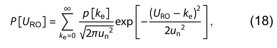
2.Signal chain model
2.1.Basic concepts
The signal chain model of single-bit and multi-bit QISs is illustrated in Fig.2, which contains signal conversion processes of photons to electrons, electrons to voltages, and voltages to digital numbers.The parameters of the signal chain model in Fig.2 are listed in Table 1.
As shown in Fig.2 and Table 1, the input and output signals of the proposed model arekphand DN, respectively.Inthe jot,kphincident photons arrive at the pinned photodiode and generatekphephotoelectrons on the condition that the quantum efficiency of the jot is QE.Then,kphephotoelectrons andkddark signal electrons, which are generated from dark current, constitute togetherketotal signal electrons.Then,ketotal signal electrons are transferred to the floating diffusion and converted toVCGon the condition that the conversion gain of the jot is CG.In the readout circuit,VCGis converted toVROon the condition that the read noise of the readout circuit isvn.In the ADC,VROis converted to DN on the condition that the quantizer threshold of the ADC isvth.

Table 1. The parameters of the signal chain model in Fig.2.
It is noted that the electron-referred values (i.e., the normalized values) ofVCG,VRO,vn, andvthareUCG,URO,un, anduth, respectively.In most cases, the normalized values are introduced because it is more convenient to use them in mathematical derivation.The unit of ro (i.e., ADU) is equivalent to p or e-, when the ADC output digital numbers are compared with photons or photoelectrons.To analyze the proposed signal chain model mathematically, a series of probability distributions are introduced in the following sections.
2.2.Total signal electrons
In the proposed signal chain model, the total signal electrons consist of photoelectrons and dark signal electrons,which are generated from incident photons and dark current in the jot, respectively.As described in Refs.[13, 18], benefiting from the jot device structure and the QIS operating characteristic, the image lag and crosstalk of pump-gate jots in the QIS are acceptable for photon counting and photoelectron counting applications under different exposure levels.Therefore, other sources of total signal electrons, including image lag, optical crosstalk, and electronic crosstalk, are not considered in the proposed model.
The emission of photons from most light sources is welldescribed by Poisson distribution[9].Thus, over the integration timeτ, the probability mass function (PMF) thatkphinciden t photons arrive at the jot is defined as:whereμphis the mean value of incident photons, andkphis a nonnegative integer.

The quantum efficiency of the jot QE is defined as the number of photoelectrons divided by the number of incident photons.The process that photons convert to photoelectrons obeys binomial distribution[7].Thus, the PMF thatkphephotoelectrons generate fromkphincident photons under QE is defined as:
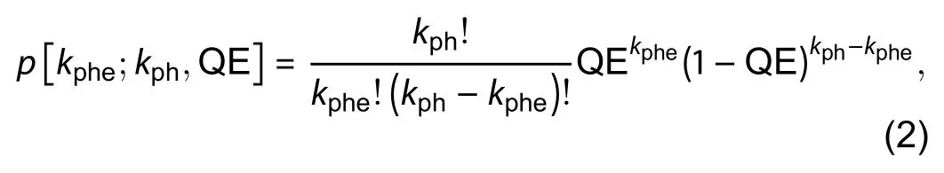
wherekpheandkphare nonnegative integers, andkpheis less than or equal tokph.
Then, the PMF thatkphephotoelectrons are generated in the jot underμphand QE, which is the convolution of two mutually independent PMFs Eqs.(1) and (2), is derived as:
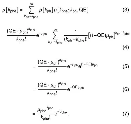
wherep[kphe]obeys Poisson distribution, andμpheis the mean value of the photoelectrons.
Similarly, the emission of dark signal electrons that generate from dark current in active pixels also obeys Poisson distribution.Thus, over the integration timeτ, the PMF thatkddark signal electrons are generated in the jot is defined as:
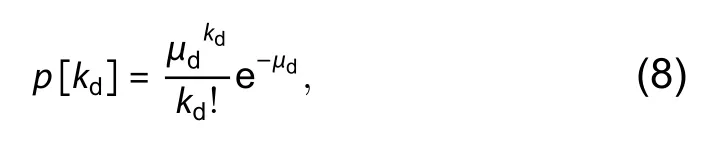
whereμdis the mean value of dark signal electrons, andkdis a nonnegative integer.
Then, the PMF thatketotal signal electrons are generated in the jot, which is the convolution of two mutually independent PMFs Eqs.(7) and (8), is derived as:
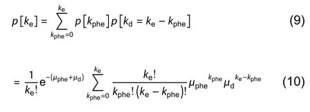

wherep[ke]also obeys Poisson distribution,μeis the mean value of total signal electrons, andkeis a nonnegative integer.
2.3.Normalized jot output
The total signal electrons are transferred from pinned photodiode (PPD) to floating diffusion (FD) and converted toVCGin the jot, when the conversion gain of the jot is CG that is calculated as:

whereqis the electron charge,CFDis the total capacitance of FD, and the unit of CG is usuallyμV/e-.
Then, the voltage-referred jot output is defined as:

It is convenient to use normalized values to simplify the analysis of the proposed model.Thus, the normalized value(i.e., the electron-referred value) ofVCGis calculated as[10]:
In the subsequent derivation, a similar method is used to convert the voltage-referred valuesVRO,vn, andvthto the normalized valuesURO,un, anduth, respectively.
2.4.Normalized readout circuit output
The readout circuit in the proposed model contains the source follower (SF), the amplifying circuit, and the correlation double sampling (CDS) circuit before the ADC.The voltage-referred read noise of the readout circuitvn, which contains thermal noise and 1/fnoise, is normalized as[10]:
It is noted that only temporal noise is considered in the proposed model.In other words, the spatial noise (i.e., fixed pattern noise (FPN), including dark signal nonuniformity(DSNU) and photoresponse nonuniformity (PRNU)), which may cause by QE, CG,un, anduthnonuniformities among jots array, are not considered in the proposed model.
The main approach of the QIS to achieve photon counting and photoelectron counting is to increase the conversion gain of jots to reduce the electron-referred read noise lower than 0.5 e- r.m.s.(i.e., deep sup-electron read noise level).For example, whenvnis equal to 100μV r.m.s., CG is required to be higher than 200μV/e-, i.e.,CFDis required to be lower than 0.8 fF, to make sureunis lower than 0.5 e- r.m.s..
When the read noiseunobeys Gaussian distribution, the component probability density function (PDF) that the normalized readout circuit outputUROgenerates from the normalized jot outputUCGis defined as[10]:

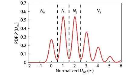
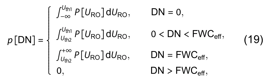
Fig.3.(Color online) The PDF P[URO]as a function of URO on the condition that μe = 2 e- and un = 0.2 e- r.m.s..N0, N1, N2, and N3 are four quantization levels corresponding to 0, 1, 2, and 3 ADU for a 2-bit QIS.The dashed lines are three quantization boundaries corresponding to 0.5,1.5, and 2.5 e- for a 2-bit QIS.
Using Eqs.(12), (14), (15), and (17), the PDF that the normalized readout circuit outputUROis generated, when the mean value of total signal electrons isμe, is derived as:
whereUROis a real number.
The PDFP[URO]as a function ofUROon the condition thatμe= 2 e- andun= 0.2 e- r.m.s.is shown in Fig.3 as an example.
2.5.ADC output
In the process of quantization, the normalized readout circuit outputUROis converted to the ADC output DN based on different quantization levels.For ann-bit QIS, there are 2nquantization levels and 2n– 1 quantization boundaries.The effective full well capacity of the QIS is generally limited by the bit depth of ADC and equal to 2n– 1.
As shown in Fig.3, for a 2-bit QIS, four quantization levels areN0,N1,N2, andN3, which correspond to 0, 1, 2,and 3 ADU, respectively.When the normalized quantizer thresholduth= 0.5 e-, three normalized quantization boundaries are 0.5, 1.5, and 2.5 e-.WhenURO∈(–∞, 0.5 e-], DN = 0 ADU; whenURO∈(0.5 e-, 1.5 e-], DN = 1 ADU; whenURO∈(1.5 e-, 2.5 e-], DN = 2 ADU; whenURO∈(2.5 e-, +∞], DN = 3 ADU.
Thus, for ann-bit QIS, the PMF that the ADC output digital numbers DN is generated, when the normalized quantizer threshold isuth, is defined as:
where the higher quantization boundaryUth1= DN +uth, the lower quantization boundaryUth2= DN – (1 –uth), the effective full well capacity FWCeff= 2n– 1, and DN is a nonnegative integer.
3.Photoresponse characteristic
Conventional CISs generally have linear response, and some CISs can achieve logarithmic and linear-logarithmic response through pixel or circuit structure design.In contrast from these CISs, the QIS has a special photoresponse characteristic, which is referred to asD–logHresponse.For high dynamic range applications, the overexposure latitude range of theD–logHresponse curve is used to extend the dynamic range of the QIS[9].For applications that need high accuracy photon counting and photoelectron counting, the high accuracy linear range of theD–logHresponse curve is required to be determined in theory.
3.1.Ideal D–logH photoresponse curves
As shown in Fig.1, by reconstructing a specified spatialtemporal data cube of jots into a single data point of a pixel in the output image, the trade-off between the equivalent full well capacity, spatial resolution, and temporal resolution can be flexibly achieved.The spatial and temporal oversampling coefficients of the QIS are defined asMSandMT, respectively, and the total oversampling coefficient of the QIS is calculated as:

whereMhas various spatial-temporal combinations.For example, whenM= 512, a 4 × 4 × 32, 8 × 8 × 8, 16 × 16 × 2,et al.sub-cube of jots is alternative.
Assuming the jots used for reconstruction are completely equivalent (i.e., no DSNU and PRNU among jots array),the signal value of ADC output is calculated as:
Similarly, the saturated signal value of ADC output is calculated as:
where FWCequand FWCeffis the equivalent and effective full well capacity respectively, andnis the bit depth of QISs (i.e.,the bit depth of ADCs in those QISs).For example, for a 3-bit QIS, whenMS= 4 × 4,MT= 8 andM= 4 × 4 × 8 = 128,FWCequ=M· FWCeff= 896 e-.
In Ref.[9], in theD-logHfunction,Hdenotes quanta exposure, which is defined as the average number of photons or photoelectrons arrive at a jot over the integration period; andDdenotes bit density, which is defined as the number of saturated jots divided by the number of total jots for 1-bit QISs.
In this paper, theD–logHfunction is extended ton-bit QISs.Hdenotes quanta exposure, which is defined as the mean value of photons that arrive at a jot over the integration timeτ.Thus,His equal toμph.When QE = 1 e-/p,His also equal toμphe× 1 p/e-.Meanwhile,Ddenotes signal density, which is defined as:
whereSDNandSDN,satare given by Eqs.(21) and (22) respectively.
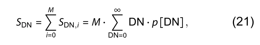
The idealD-logHresponse curves for 1-bit, 2-bit, 3-bit, 4-bit, and 5-bit QISs are shown in solid lines in Fig.4, whereQE = 1 e-/p,μd= 0 e-,un= 0 e- r.m.s., anduth= 0.5 e-.The ideal linear response curves for 1-bit to 5-bit CISs are shown in dashed lines in Fig.4, where the output signal is equal to the input signal (i.e., the ideal accuracy photon counting is achieved).
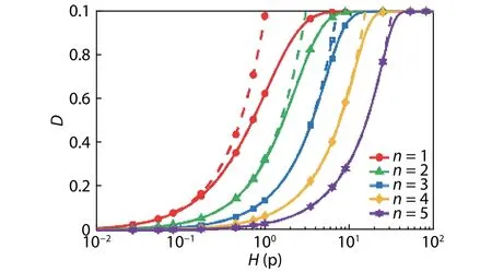
Fig.4.(Color online) The ideal D-logH response curves for 1-bit to 5-bit QISs in solid lines.And the ideal linear response curves for 1-bit to 5-bit CISs in dashed lines.

Table 2. Different conditions for realistic QISs in Figs.5, 7, and 8.
As shown in Fig.4, whenD= 0.99, the saturated quanta exposureHsatof 1-bit to 5-bit QISs are equal to 4.7, 7.3, 13,22, and 39 p, respectively.Meanwhile,Hsatof 1-bit to 5-bit CISs are equal to 0.99, 2.97, 6.93, 14.85, and 30.69 p, respectively.Thus, compared with then-bit CIS, then-bit QIS has a higherHsatand a greater potential in HDR applications in theory.
AsHincreases from 0.01 to 100 p, the QIS gradually enters in the nonlinear response range (the non-overlap range of solid line and dashed line) from the linear response range (the overlap range of solid line and dashed line).Asnincreases from 1 to 5, the linear and nonlinear response ranges of 1-bit to 5-bit QISs are extended and narrowed respectively.Thus, QISs with higher bit depth are inferred to have a better performance in applications that need high accuracy photon counting and photoelectron counting in theory.
3.2.Realistic photoresponse curves
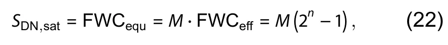
For realistic QISs, QE < 1 e-/p,μd> 0 e-,un> 0 e- r.m.s.,anduth= 0.5 e-.In the realistic response curve for ann-bit QIS,His equal toμph, andDis calculated as Eq.(23).The realistic response curves for the 3-bit QIS under five different conditions, which are listed in Table 2, are shown in Fig.5.
Based on Fig.5, the effects of QE,μd, andunto realistic response curves for the QIS are qualitatively analyzed, as follows:
(1) Curve 1 (ideal) is the ideal response curve for the 3-bit QIS as a comparison;
(2) Curve 2 (QE = 0.8 e-/p) can be approximatively considered to be obtained by shifting curve 1 to the right.This means that when QE < 1 e-/p, a higherHis required to get the sameDin curve 1;

Fig.5.(Color online) The realistic response curves for the 3-bit QIS.The different conditions of curve 1 to 5 are listed in Table 2.
(3) In curve 3 (μd= 0.01 e-), asHincreases from 0.01 p to 100 p, curve 3 gradually coincides with curve 1, the difference ofDbetween curve 3 and curve 1 gradually decreases,i.e.,μd> 0 e- has an obvious effect on low light level (H<0.1 p);
(4) In curve 4 (un= 0.3 e- r.m.s.),un> 0 e- r.m.s.has a similar effect on low light level (H< 0.1 p) compared withμd> 0 e- in curve 3;
(5) Curve 5 (QE = 0.8 e-/p,μd= 0.01 e-, andun= 0.3 er.m.s.) combines the effects of QE < 1 e-/p,μd> 0 e-, andun>0 e- r.m.s..WhenHis lower than 0.25 p,Din curve 5 is higher than curve 1,μd> 0 e- andun> 0 e- r.m.s.are dominant.WhenHis higher than 0.25 p,Din curve 5 is lower than curve 1, QE < 1 e-/p is dominant.
In summary, the lower boundary of the linear response range of the QIS is limited byμdandun, the higher boundary of the above range is limited by the bit depth of QISsn, and this range shifts to the right when QE < 1 e-/p.To further study the high accuracy linear ranges towards photon counting and photoelectron counting of ideal and realistic response curves, and the effects of QE,μd, andunto the above ranges of realistic response curves, a quantitative analysis is performed in Section 4.
4.Signal error rate
In this paper, the signal error rate is defined as the absolute value of the difference between the input and output signals divided by the input signal, which is used as the qualifying factor to evaluate the accuracy of photon counting or photoelectron counting for the QIS.
4.1.Signal error rate for ideal QISs
Assuming that the jots used for reconstruction are completely equivalent, like Eq.(21), the signal value of incident photons is calculated as:

Similarly, the signal value of photoelectrons is calculated as:

And the signal error rate betweenSDNandSphis defined as:

Fig.6.(Color online) The photon counting signal error rate SERph as a function of the mean value of incident photons μph for ideal 1-bit to 5-bit QISs.

where SERphis the qualifying factor of evaluating the accuracy of photon counting in the QIS.When SERphis decreased,the difference betweenSDNandSphis decreased, and the accuracy of photon counting is increased.
The signal error rate betweenSDNandSpheis defined as:
where SERpheis the qualifying factor of evaluating the accuracy of photoelectron counting in the QIS.When SERpheis decreased, the difference betweenSDNandSpheis decreased,and the accuracy of photoelectron counting is increased.
In this paper, based on Eqs.(26) and (27), theμphvalue interval corresponding to SERph< 0.01 is defined as the high accuracy photon counting exposure range (hereinafter to be referred asRph) or high accuracy linear range of response curves, and theμphevalue interval corresponding to SERphe<0.01 is defined as the high accuracy photoelectron counting exposure range (hereinafter to be referred asRphe).
As forn-bit ideal QISs, QE = 1 e-/p,μd= 0 e-,un= 0 er.m.s., anduth= 0.5 e-.In this case,μphe=μph× 1 e-/p, and SERphe= SERph, i.e., photon counting is equivalent to photoelectron counting when QE = 1 e-/p.And SERphas a function ofμphfor ideal 1-bit to 5-bit QISs is shown in Fig.6.
As shown in Fig.6, for a givenn, whenμphis increased,SERphis increased; for a givenμph, whennis increased, SERphis decreased; for ideal 1-bit to 5-bit QISs,Rphis (–∞, 0.021 p),(–∞, 0.72 p), (–∞, 3.4 p), (–∞, 10 p), and (–∞, 25 p), respectively; in other words, asnincreases from 1 to 5,Rphis extended from (–∞, 0.021 p) to (–∞, 25 p).
Based on these results, it can be proven theoretically that increasing the bit depth of the QIS is an effective approach to improve the performance of QISs in applications that need high accuracy photon counting and photoelectron counting.
4.2.Photon counting signal error rate for realistic QISs
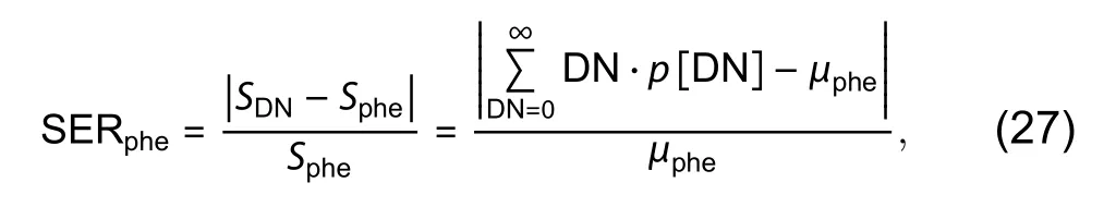
As forn-bit realistic QISs, QE < 1 e-/p,μd> 0 e-,un> 0 er.m.s., anduth= 0.5 e-.In this case, photon counting is inequivalent to photoelectron counting.To determine theRphof realistic QISs, SERphas a function ofμphfor the 3-bit QIS under five different conditions, which are listed in Table 2, is shown in Fig.7.
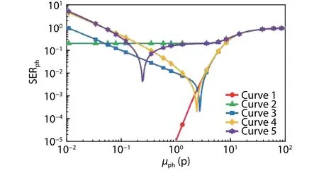
Fig.7.(Color online) The photon counting signal error rate SERph as a function of the mean value of incident photons μph for the 3-bit QIS.The five conditions of curve 1 to 5 are listed in Table 2.
Based on Fig.7, theRphof curve 1 to 5 is (–∞, 3.4 p), N/A,(0.99 p, 3.6 p), (1.2 p, 3.4 p), and (0.23p, 0.26p), respectively.And the effects of QE,μd, andunto theRphof the realistic QIS are quantitative analyzed as follows:
(1) Curve 1 (ideal) is the ideal SERphcurve for the 3-bit QIS as a comparison;
(2) In curve 2 (QE = 0.8 e-/p), whenμph≤ 1.6 p, SERphremains constant at 0.2; whenμph> 1.6 p, SERphis gradually increased to 1.This means that QE has significant effect on SERph, and QE is the main limit factor of high accuracy photon counting for the QIS;
(3) In curve 3 (μd= 0.01 e-), asμphincreases from 0.01 p to 100 p, SERphfirst decreases from a high value to the minimum value and then gradually increases to 1.The minimum value point (i.e., the optimal point for photon counting) is(μph= 2.7 p, SERph= 2.23 × 10⁻⁴).Compared with curve 1,μd> 0 e- mainly increases the SERphon low light level (H< 0.1 p);
(4) In curve 4 (un= 0.3 e- r.m.s.),un> 0 e- r.m.s.has a similar effect on SERphcompared withμd> 0 e- in curve 3.The minimum value point of curve 4 is (μph= 2.4 p, SERph= 2.14 ×10⁻⁴);
(5) In curve 5 (QE = 0.8,μd= 0.01 e-, andun= 0.3 er.m.s.), the effects of QE < 1 e-/p,μd> 0 e-, andun> 0 er.m.s.are combined.Asμphincreases from 0.01 p to 100 p,SERphfirst decreases and then increases.The minimum value point of curve 5 is (μph= 0.24 p, SERph= 4.37 × 10⁻³).Whenμph< 0.13 p, SERph> 0.2, the effects ofμd= 0.01 e- andun=0.3 e- r.m.s.are dominant; when 0.13 p ≤μph≤ 3.5 p, 4.37 ×10⁻³≤ SERph≤ 0.2, the effect of QE = 0.8 e-/p is dominant;whenμph> 3.5 p, SERphis gradually increased to 1 due to the saturation of jots.
The cause of optimal point in curve 5 can be explained through the following example:assuming that 10 photons arrive at the jot and convert to 9 photoelectrons under QE; if 1 dark signal electron is generated, then the number of total signal electrons is 10; thus, a dark signal electron may fill the electron loss due to QE and cause SERphdecrease in some special cases.
In summary, when QE is low,Rphis limited by QE; when QE is high enough, such as 0.95 e-/p[7], the lower boundary ofRphis limited byμdandun, and the higher boundary ofRphis limited by the saturated quanta exposure (i.e., the bit depth of QISs).Therefore, the main approach of extending theRphof realistic QISs is increasing QE andn, and decreas-ingμdandun.

Fig.8.(Color online) The photoelectron counting signal error rate SERphe as a function of the mean value of incident photons μph for the 3-bit QIS.The five conditions of curve 1 to 5 are listed in Table 2.
4.3.Photoelectron counting signal error rate for realistic QISs
To determine theRpheof realistic QISs, SERpheas a function ofμphfor the 3-bit QIS under five different conditions,which are listed in Table 2, is shown in Fig.8.
As shown in Fig.8, theRpheof curve 1 to 5 is (–∞, 3.4 p),(–∞, 4.3 p), (0.99 p, 3.6 p), (1.2 p, 3.4 p), and (2.1 p, 4.5 p), respectively.It is noted that since QE = 1 e-/p and SERphe=SERph, curve 1, 3, and 4 in Fig.8 are the same as Fig.7.
Curve 2 (QE = 0.8 e-/p) can be approximatively considered to be obtained by shifting curve 1 (ideal) to the right(i.e.,Rpheshifts to the right when QE < 1 e-/p).
In curve 5 (QE = 0.8 e-/p,μd= 0.01 e-, andun= 0.3 er.m.s.), the effects of QE < 1 e-/p,μd> 0 e-, andun> 0 e- r.m.s.are combined.Asμphincreases from 0.01 to 100 p, SERphefirst decreases and then increases.The minimum value point of curve 5 is (μph= 3.5 p, SERphe= 1.45 × 10⁻⁴).Whenμph<3.5 p, SERphe> 1.45 × 10⁻⁴, the effects ofμd= 0.01 e- andun=0.3 e- r.m.s.are dominant; whenμph≥ 3.5 p, curve 5 gradually overlaps with curve 2, and SERpheis finally increased to 1 due to the saturation of jots.
In summary, the lower boundary ofRpheis limited byμdandun, the higher boundary ofRpheis limited by the bit depth of QISs, andRpheshifts to the right when QE < 1 e-/p.Therefore, the main approach of extending theRpheof realistic QISs is increasingn, and decreasingμdandun.
5.Integration time optimization
5.1.Physical explanation
As discussed in Section 4, by calculating SERphand SERphe, theμphandμphevalue interval corresponding to SERph< 0.01 and SERphe< 0.01 (i.e.,RphandRphe) are determined.
In imaging applications, under the specified illuminance level and pixel size, by adjusting the integration time of the QIS,μphandμphecan be adjusted toRphandRphe, respectively, and the high accuracy photon counting and photoelectron counting can be achieved.
To propose the integration time optimization method,the illuminance of the light sourceIluxshould be converted to the mean value of incident photonsμphat first.
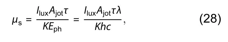
The conversion formula betweenIluxand the mean value of photons that generate from the light sourceμsis defined as[19]:
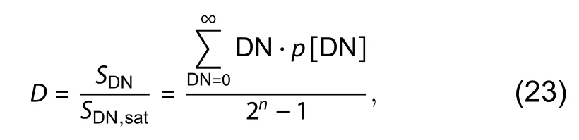
Fig.9.The conceptual illustration of the Airy disk and jot array.The Airy disk diameter DA = 3.8 μm, the jot area Ajot = 1 μm2 (left) and Ajot = 0.25 μm2 (right).
whereEphdenotes the energy of a single photon,Ajotdenotes the area of a single jot,τdenotes the integration time of jots,Kdenotes the conversion coefficient,h= 6.626 ×10⁻³⁴J∙s denotes Planck constant,c= 2.998 × 10⁸m/s denotes the speed of light in vacuum,λdenotes the wavelength of photons.
The conversion formula betweenμsandμphis defined as[19]:
whereFNdenotes the F number of lens,Tdenotes the transmittance of lens,Rdenotes the reflectance of the image sensor surface, and FF denotes the fill factor of the jots.
Whenλ= 555 nm,K= 683 lm∙W–1= 683 lux∙m2∙W–1[19],and letFN= 2.8,T= 0.9,R= 0.1, and FF = 0.9.Using Eqs.(28)and (29), the conversion formula betweenIluxandμphis calculated as:
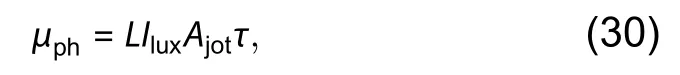
whereLis the corrected parameter of the specified QIS, andL= 9.51 × 10⁻⁵lux–1∙μm–2∙μs–1in this case.
For an ideal optical imaging system, the perfect lens focuses the point light source to a diffraction-limit spot, which is referred to as Airy disk, and the spot is surrounded by higher order diffraction rings.The diameter of Airy disk is calculated as[4]:

Whenλ= 555 nm andFN= 2.8,DA= 3.8μm.To intuitively describe the geometric dimensioning of the Airy disk and jot array, and make a physical explanation of the relationship betweenIlux,Ajot, andτ, a conceptual illustration is shown in Fig.9.
As shown in Fig.9, whenAjot= 1μm2orAjot= 0.25μm2,the same Airy disk covers 9 or 44 jots, respectively.This means that under specifiedIluxandτ, whenAjotis larger, the jot has a higher probability of collecting more incident photons.In other words, whenIluxandAjotare equal to specified values,μphorμphecan be adjusted to be withinRphorRpheby optimizing integration timeτ.
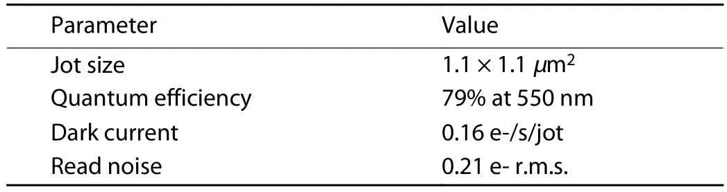
Table 3. The correlation parameters of the QIS chip in Ref.[16].
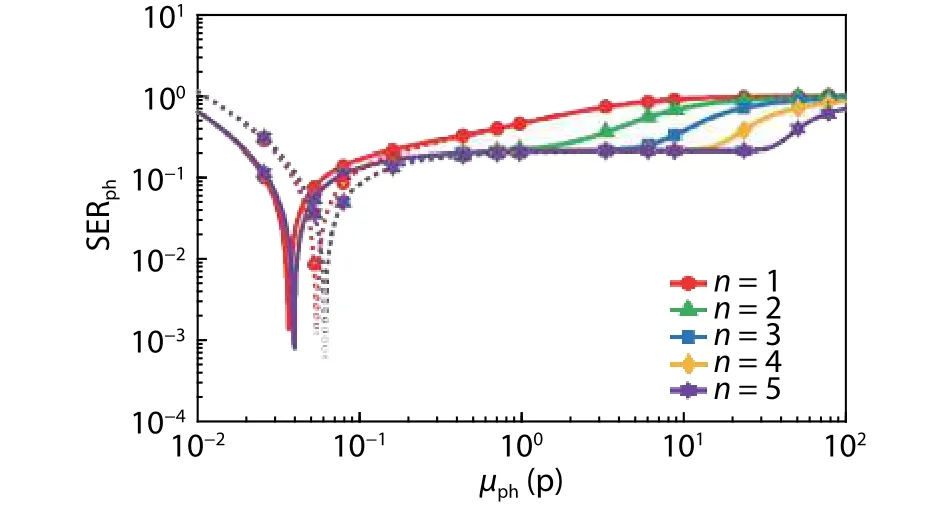
Fig.10.(Color online) The photon counting signal error rate SERph as a function of the mean value of incident photons μph for 1-bit to 5-bit QISs based on the parameters listed in Table 3.
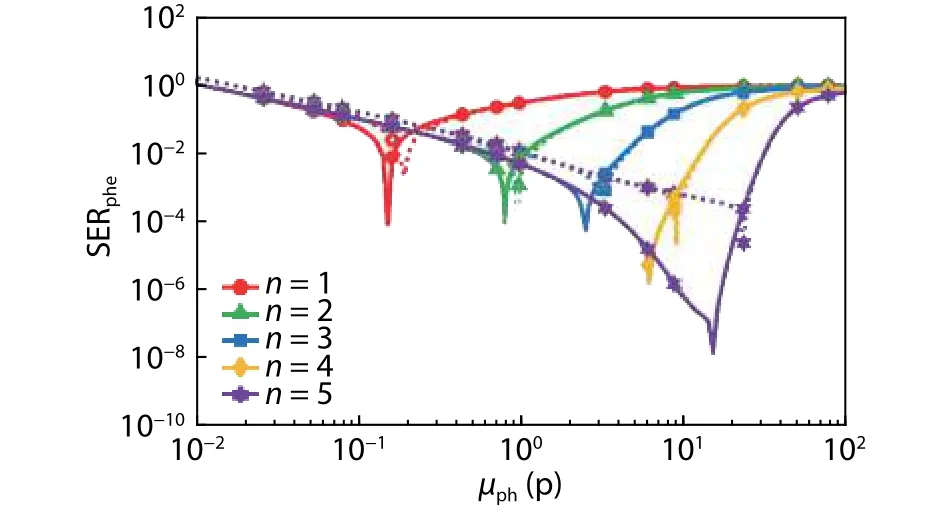
Fig.11.(Color online) The photoelectron counting signal error rate SERphe as a function of the mean value of incident photons μph for 1-bit to 5-bit QISs based on the parameters listed in Table 3.
5.2.Optimization method
To further describe the integration time optimization method for QISs, the correlation parameters of the 1 Mjot QIS chip in Ref.[16]are listed in Table 3.
Based on the parameters listed in Table 3, QE = 0.79 e-/p,μd= 1.6 × 10⁻⁶e- to 4.8 × 10⁻³e- (assumingτ= 10μs to 30 ms),un= 0.21 e- r.m.s., anduth= 0.5 e-.SERphas a function ofμphis shown in Fig.10, and SERpheas a function ofμphis shown in Fig.11.For solid lines, QE = 0.79 e-/p,μd= 1.6 ×10⁻⁶e-,un= 0.21 e- r.m.s., anduth= 0.5 e-; for dashed lines,QE = 0.79 e-/p,μd= 4.8 × 10⁻³e-,un= 0.21 e- r.m.s., anduth=0.5 e-.
As shown in Fig.10, for solid lines,Rphis (0.035 p, 0.039 p)for 1-bit QIS, andRphis (0.038 p, 0.042 p) for 2-bit to 5-bit QISs.For dashed lines,Rphis (0.052 p, 0.057 p) for 1-bit QIS,andRphis (0.059 p, 0.065 p) for 2-bit to 5-bit QISs.
As shown in Fig.11, for solid lines,Rpheis (0.13 p, 0.17 p),(0.55 p, 1.1 p), (0.65 p, 4.3 p), (0.65 p, 13 p), and (0.65 p, 31 p)for 1 to 5 bit QISs, respectively.For dashed lines,Rpheis (0.17 p,0.2 p), (0.74 p, 1.2 p), (1 p, 4.4 p), (1 p, 13 p), and (1 p, 31 p)for 1 to 5 bit QISs, respectively.
To sum up, as for the QISs in Figs.10 and 11, QE is req uired to be further increased to extendRph; the dark current in jots is small enough thatμdhas a slight effect onRpheeven for a long integration timeτ;unis required to be further decreased to extendRphe; and a higher bit depth of QISsnis suggested to extendRphe.
As listed in Table 3, the jot areaAjot= 1.21μm2.For a more advanced process,Ajotis predicted to be smaller in the future.The range ofAjotis assumed as 0.1 to 1.5μm2in this paper.In addition, the acceptable integration timeτ(hereinafter to be referred asRτ) is assumed as 10 to 30 000μs.
For the 3-bit QIS in Fig.11,Rpheis (1 p, 4.4 p).Based on Eq.(30), the relationship betweenAjot,μph, andτunder different illuminance levelIluxis shown in Fig.12.
As shown in Fig.12, the area in orange denotesτ<10μs, andτis belowRτ; the area in blue denotes 10μs ≤τ≤30 000μs, andτis within theRτ; the area in yellow denotesτ> 30 000μs, andτis aboveRτ.AsIluxincreases from 0.1 to 10 000 lux, the area in blue increases firstly and then decreases.
WhenIluxis low, such as 0.1 lux,τis required to reach a higher value that may be aboveRτ; whenIluxis high, such as 10 000 lux,τis required to reach a lower value that may be belowRτ.Thus, it will be more difficult to ensure that the QIS is working withinRphe, when the light level is too low or too high.Combined with the result in Section 4, whenRphorRpheis extended, the integration time optimization difficulty will be decreased.In addition, whenIluxis lower, a largerAjotwill decrease the optimization difficulty; whenIluxis higher, a smallerAjotwill decrease the optimization difficulty.For example,whenIlux= 1 lux andAjot= 1.21μm2, the recommended value interval ofτis (8.8 ms, 30 ms), and whenIlux= 10 000 lux andAjot= 0.21μm2, the recommended value interval ofτis (10μs, 21.3μs).
In summary, the trade-off betweenAjot,μph, andτunder differentIluxis needed to be considered, when the QIS is designed and operated.By integration time optimization, the QIS can work withinRphorRphe.The main approach of decreasing the optimization difficulty is to extendRphorRphe, which required higher quantum efficiency, higher bit depth of QISs,lower dark current, and lower read noise.Therefore, when the correlation parameters of QISs are determined, the similar integration time optimization method can be performed to guide the design and operation of QISs.
6.Conclusion
In this paper, a signal chain model of single-bit and multi-bit QISs, which contains signal conversion processes of photons, electrons, voltages, and digital numbers, is established.Based on the proposed model, the photoresponse characteristics and signal error rates of ideal and realistic QISs are investigated.The effects of the ADC bit depthn, quantum efficiency QE, the mean value of dark signal electronsμd, and electron-referred read noiseunto them are analyzed.The signal error rate between photons or photoelectrons and digital numbers SERphand SERpheare defined as the quality factors of photon and photoelectron counting.When SERphand SERpheare lower than 0.01, the high accuracy photon and photoelectron counting exposure ranges, which are referred asRphandRphe, are determined.The main approach of extendingRphandRpheis increasingnand QE, and decreasingμdandun.Moreover, an integration time optimization method to en-sure that the QIS works withinRphandRpheis presented.The trade-off between jot areaAjot, the mean value of incident photonsμph, and integration timeτunder different illuminance levelIluxare analyzed.Whenn,Ajot, QE,μd, andunof QISs are determined, the integration time optimization method can be performed to guide the design and operation of QISs.
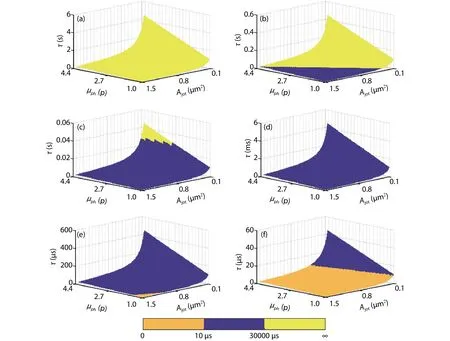
Fig.12.(Color online) The relationship between jot area Ajot, the mean value of incident photons μph, and integration time τ under different illuminance level Ilux for the 3-bit QIS in Fig.11.(a) Ilux = 0.1 lux.(b) Ilux = 1 lux.(c) Ilux = 10 lux.(d) Ilux = 100 lux.(e) Ilux = 1000 lux.(f) Ilux = 10 000 lux.
Acknowledgements
This work was supported by the Tianjin Key Laboratory of Imaging and Sensing Microelectronic Technology.
 Journal of Semiconductors2021年6期
- Journal of Semiconductors的其它文章
- Oscillation neuron based on a low-variability threshold switching device for high-performance neuromorphic computing
- A 3.3 kV 4H-SiC split gate MOSFET with a central implant region for superior trade-off between static and switching performance
- Determination of trap density-of-states distribution of nitrogendoped ultrananocrystalline diamond/hydrogenated amorphous carbon composite films
- 3.3 kV 4H-SiC DMOSFET with a source-contacted dummy gate for high-frequency applications
- Heavily doped silicon:A potential replacement of conventional plasmonic metals
- A review of manufacturing technologies for silicon carbide superjunction devices